Abstract
In recent years, additive manufacturing (AM) has played a significant role in various fashion industries, especially the textile and jewelry manufacturing sectors. This review article delves deeply into the wide range of methods and materials used to make intricately designed jewelry fabrication using the additive manufacturing (AM) process. The Laser Powder Bed Fusion (L-PBF) process is examined for its suitability in achieving complex design and structural integrity in jewelry fabrication even with respect to powder metallurgy methods. Moreover, the review explores the use of precious materials, such as gold, silver, copper, platinum, and their alloys in additive manufacturing. Processing precious materials is challenging due to their high reflectivity and thermal conductivity, which results in poor densification and mechanical properties. To address this issue, the review article proposes three different strategies: (i) adding alloying elements, (ii) coating powder particles, and (iii) using low-wavelength lasers (green or blue). Finally, this review examines crucial post-processing techniques to improve surface quality, robustness, and attractiveness. To conclude, this review emphasizes the potential of combining additive manufacturing (AM) with traditional craftsmanship for creating jewelry, exploring the potential future directions and developments in the field of additive manufacturing (AM) for jewelry fabrication.
1. Introduction
Even though plenty of manufacturing processes are available for making jewelry components, additive manufacturing processes are preferred to subtractive manufacturing processing to reduce material wastage. Additive manufacturing (AM) is also known as 3D printing, rapid prototyping, layer-by-layer manufacturing, digital manufacturing, or solid-free form manufacturing processing, and it is used for the fabrication of intricate geometries from 3D model data [1]. AM was developed as a potential tool of fabrication as compared to the traditional manufacturing (TM) method because it has design flexibility, customization features, the ability to create complicated shapes, and wastage reduction. This technology uses layer-by-layer printing to create items with robust mechanical quality [1,2]. According to ISO/ASTM 52900:2015(E), there are two main types of AM processes: (i) single-step AM processes and (ii) multi-step AM processes [3]. In the first case, independently of the techniques, the work material may achieve its fundamental form and expected qualities in a single phase. Layer after layer, parts in metal, polymer, and composite materials can be built up over time. The adhesion principle is generally used in multi-step AM processes to create the intended part geometry, and then additional stages are used to create the part’s desired qualities. For instance, it is possible that the geometry was first acquired through the joining of metallic, ceramic, and composite elements. They could go through further processes, like sintering or infiltration, to obtain the desired qualities later [4,5,6]. A thorough analysis of the AM process was provided by Parupelli and Desai, which focused on the recent advancements made by numerous researchers and industries. A summary of the features, benefits, and drawbacks of each AM printing method was reported and presented in their work. The key advancements in AM technology in various industries, including electronics, medical, aerospace, automotive, and construction industries, were also examined [7].
The main focus of this review is on jewelry production, to emphasize, on the basis of published work on the subject [8], the potential that these new technologies may have for the jewelry industry compared to traditional methods (TM). AM offers the advantage of allowing greater design freedom, creating innovative and complex designs that would otherwise be challenging to construct using conventional techniques [9]. This is not the only important aspect. A clear example of the potentiality of AM is presented in Figure 1, Figure 2 and Figure 3. A gold pendant piece “the Ojo” was constructed using Laser Powder Bed Fusion (L-PBF) with the help of a support structure [10]. The supporting structure for making the jewelry was designed using CAD software (Figure 1). Figure 2 reports the fabrication step (processing) of the Au jewelry while Figure 3 underlines the surface finishing that can be obtained by additional polishing treatment (post-processing) [10]. The complexity of the part and its manufactured cost are directly correlated in the current standard jewelry manufacturing process; however, by using L-PBF methods, this relationship can be greatly reduced compared to the conventional method.
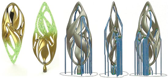
Figure 1.
Support structures designed using CAD software for “the Ojo”, Reprinted with permission from ref. [10]. 2016 Springer Nature.
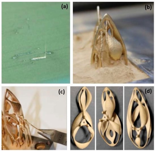
Figure 2.
(a) Laser beam on thinly spread Au powder using the L-PBF process, (b) “the Ojo” pendant built from the Au powder bed, (c) support remotion by pliers, (d) three different pendants before mechanical finishing and polishing, Reprinted from ref. [8].
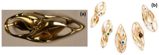
Figure 3.
(a) “The Ojo” hand polished after 1 h stream finishing, (b) “the Ojo” series after mechanical and hand polishing and further stone setting, Reprinted with permission from ref. [10]. 2016 Springer Nature.
In the L-PBF production, in fact, around 30% of extra material was processed to create the support structure (in some geometries, this amount can be decreased to virtually 0%). In the TM, such as lost wax castings, the extra material is close to 60% and even if this value can be decreased by optimizing the casting piece ratio, it can never reach L-PBF values. Telma Ferreira et al. reported that L-PBF was an alternate and more efficient technique to fabricate jewelry components while reducing material costs and production time as compared to TM. In fact, comparing the processing time of silver and stainless-steel jewelry fabricated by TM and AM, AM jewelry (3 weeks) was made faster than TM jewelry (more than 10 weeks) [11,12,13].
Based on previous literature, this review discussed the current state of the art of AM for jewelry applications. Furthermore, the future direction of AM for Industry 4.0 jewelry manufacturing is outlined (Figure 4).
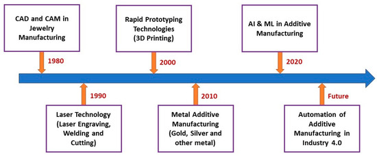
Figure 4.
Current and future trends in AM of the jewelry industry.
2. Powder Metallurgy (PM) and Advanced Manufacturing (AM) Techniques Used for Jewelry Fabrication
Traditional jewelry manufacturing incorporates established methods that perfectly blend timeless craftsmanship with precision techniques. The process involves traditional steps such as design conception, material selection, and model creation. Essential activities such as casting, wax carving, and handcrafting play a key role in ensuring meticulous detail.
Without dwelling on these traditional methods, which have very long lead times, this paragraph discusses the advantages and disadvantages of powder metallurgy and AM techniques for metal jewelry fabrication (Figure 5).
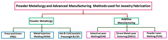
Figure 5.
Innovative technique for jewelry production: powder metallurgy and advanced manufacturing methods.
Both PM and AM technologies depend on powdered materials with well-defined properties and morphology to ensure the quality and performance of the final products. In these technologies, the powder characteristics, such as particle shape, particle size distribution, apparent and packing density, flowability, and morphology are crucial. These factors impact the powder behavior during processing, thereby affecting the mechanical properties and accuracy of the finished part. In particular, spherical particles (Figure 6) of well-controlled grain size are generally preferred due to their better flowability and packing density. To obtain these powder characteristics, gas atomization is a widely used method for producing metal powders with the desired properties for both PM and AM. In this process, molten metal is dispersed into fine droplets by a high-pressure gas stream, typically argon or nitrogen, which solidify into powder particles as they cool. Gas atomization produces highly spherical powders with controlled particle size distribution, and minimal contamination, making it a suitable technique for generating high-quality powders for these technologies [14,15].
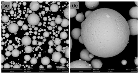
Figure 6.
SEM image of commercial copper powder fabricated by gas atomization processes with lower magnification (a) and higher magnification (b).
2.1. Powder Metallurgy Method Used for Jewelry Fabrication
In addition to the traditional techniques, powder metallurgy (P/M) refers to the net-shape manufacturing of components using powdered metal. Various techniques within powder metallurgy, such as press and sinter (P&S), metal injection molding (MIM) and hot and cold isostatic pressing (HIP and CIP) were recently investigated [16,17]. In particular, powder metallurgical processing finds widespread applications in jewelry which show a quality comparable to cast parts. The primary advantage lies in the reduced part cost due to minimized material waste and processing expenses. Consequently, the direct application of powder metallurgy in jewelry fabrication offers significant benefits [16,17]. Peter M. Raw first presented the pioneering development of a powder metallurgical method for large-scale ring manufacturing. Initially focused on carat-gold rings and later extended to platinum, the ring fabrication process involved steps such as powder atomization, cold pressing, sintering, and rolling to achieve the desired ring dimension. The rings produced by powder metallurgy have a fine grain microstructure, which contributes to improved wear resistance and strength. The fine grain size, often observed in powder metallurgical products, was attributed to the existence of an extremely fine, sub-microscopic porosity that has the potential to stabilize grain boundaries. Consequently, the method has both economic and technical advantages, marking a significant milestone in ring manufacturing [18]. J. T. Strauss explored P/M technologies demonstrating their ability to create high-quality jewelry at reduced costs compared to conventional casting and machining processes. Despite this potential, the use of P/M in the jewelry industry has remained limited. The current status of P&S and MIM in the jewelry production industries was also examined by Titan and Hilderbrand, that employed press and sinter (P&S) and MIM techniques to fabricate Tanishq pure gold coins and 18-karat gold 3N pieces (Figure 7) [19,20]. Sintering, a heat treatment process that involves the consolidation of powdered materials under an optimized thermal cycle, offers numerous methods for seamlessly combining a variety of colors. K. Wiesner reported [21] that the sintering method has already been firmly established in the manufacturing of wedding rings (Figure 8).
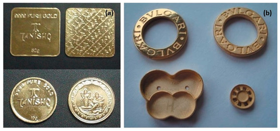
Figure 7.
(a) Press and sinter of Tanishq pure gold coins by Titan, (b) MIM-produced 18-karat gold 3N pieces, Reprinted from ref. [19].
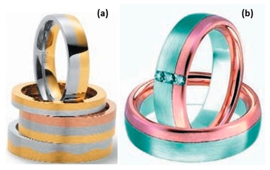
Figure 8.
(a,b) Multi-color rings, Reprinted from ref. [21].
The major disadvantage of these techniques is, of course, the simplicity of design that can be achieved by having to go through a pressing process. To enhance the process mechanism as much as possible, the optimal process parameters, such as compacting pressure and temperature, have to be identified.
2.2. Additive Manufacturing (AM) of Jewelry
In this section, the production of jewelry by means of Laser Powder Bed Fusion technology (L-PBF) is discussed in detail, bearing in mind that, in the bibliography, this technology can also be referred to as selective laser melting (SLM, a term introduced by the Fraunhofer Institute in 1995), direct metal laser melting (DMLM, a process patented in 1994 by EOS) or, finally, as laser powder melting (PLM).
L-PBF operates by employing a high-power laser to selectively melt and fuse metal powder, thereby incrementally building up parts layer-by-layer [22]. L-PFB technology is characterized by several variables that have to be optimized to increase the mechanical and physical properties of finished goods. The main factors include laser power, scanning speed, and powder layer thickness that are corrected by the Equation (1):
where p is the power, v is the scanning rate, h and l are the line offset and the layer thickness, respectively.
However, the selection of suitable L-PBF process parameters for jewelry alloys posed a considerable challenge due to the notably high thermal conductivities and reflectivities inherent in these metals and their alloys. Figure 9a provides a comparative analysis of the reflectivity of polished metal surfaces across various metal families and laser wavelengths. Reflectivity values for Au, Ag, and Cu exceeded 90% within the YAG laser wavelength (~1 μm), while cobalt, nickel, and iron fell within the 60–70% range. Although these specific reflectivity values pertained to polished solid-material surfaces, molten metal surfaces and powder particles would exhibit similarly absorption values. Consequently, in the case of Au-, Ag-, and Cu-based materials, a considerably larger percentage of the laser beam energy was reflected back rather than being absorbed as heat, as depicted in Figure 9b [22].
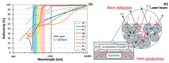
Figure 9.
(a) Comparison of different materials reflectivity, Reprinted from ref. [23] and (b) heat absorption and reflection of powder bed by the laser beam, Reprinted from ref. [22].
The local absorption of heat and energy by the powder was facilitated by the reflection of some of the incident laser energy between the surfaces of the adjacent powder particles. Subsequently, the locally absorbed heat from the powder was conducted into neighboring regions, comprising both the previously melted layers and the unmelted powder (Figure 9b). In order to achieve satisfactory processing of Au-, Ag- and Cu-based alloys with minimal residual porosity, combinations such as higher YAG laser power, lower scanning speed, lower layer thickness and shorter hatching distance had to be carefully considered [22].
In the following sections, the results that can be obtained using L-PBF on gold, silver, platinum and copper-base alloys, were discussed highlighting which strategies were used to increase laser absorption and thus achieve maximum densification.
2.2.1. AM of Gold Material
Additive manufacturing, especially L-PBF, was most suitable for fabricating gold jewelry to achieve complex and customizable designs that are otherwise too time-consuming and challenging to fabricate with the powder metallurgy method. L-PBF selectively melts the metal powder layer-by-layer to produce the bulk structure, which is guided by the 3D CAD models. Fischer-Buehner et al. fabricated 18 K yellow-gold (18 K YG) jewelry with different process parameter combinations using L-PBF. Figure 10 illustrates the impact of laser power on 18 K yellow-gold powder. The laser power was varied between 50 and 95 W, with a layer thickness of 20 μm and scanning rates ranging from 200 to 400 mm/s. In Figure 10a, it is evident that a 50 W laser power, with parameters similar to those commonly used for cobalt-chrome or steel, results in poor densification. However, the images in Figure 10b–d demonstrate that the increase in the laser power leads to an improved densification. A final laser power of 95 W yields low residual micro-porosity levels. Using the optimized parameters, the authors printed jewelry in 18 K YG as shown in Figure 10e–h. Metallographic cross sections confirm that excellent surface quality can be achieved, even with a low residual amount of microporosity [22].
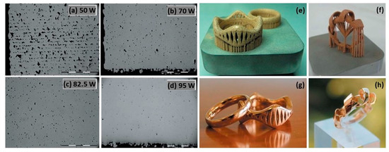
Figure 10.
SEM images of 18 K YG (a–d) obtained by L-PBF with different laser power and (e–h) jewelry parts, Reprinted from ref. [22].
Mushtaq Khan et al. presented the use of L-PBF with 24 K gold powder. Au cubes were created using a set of optimized parameters (laser powder of 50 W, hatch distance of 80 μm, layer thickness of 100 μm, and scanning speed of 65 mm/s). The hardness and the porosity of the gold cubes were examined but the analysis underlined that, even after the optimization process, a full densification cannot be obtained due to the decreased energy absorption by the gold powder, which prevents full fusion with the preceding layer, leaving inter-layer porosity. Reducing the layer thickness from 100 to 50 μm or changing the hatch distance did not significantly affect the density of the gold cubes [24]. Similarly, Zito et al. [25,26] reported the fabrication of 18 K gold alloy by L-PBF and the outcome was a reduction in strength, hardness, and high roughness compared to conventional casting processes. In particular, the hardness of 18 K palladium white gold is 174 ± 5 Hv (conventional) versus 154 ± 2 Hv (L-PBF); the ultimate tensile strength is 480 ± 25 MPa (conventional) versus 460 ± 39 MPa (L-PBF), and elongation to failure is 33 ± 9% (conventional) versus 21 ± 8% (L-PBF). However, the authors also reported that the production time for one piece is 34 h (conventional) versus 2 h (L-PBF); for ten pieces, 34.5 versus 8 h, respectively; for one hundred pieces, 37.5 versus 78.5 h, respectively underlining the main field of application of AM which becomes competitive for small batches of high geometric complexity. For mass production, the high productivity time that characterized L-PBF also brings a higher market price per gram (EUR 4–12) as compared to the conventional method (EUR 0.2–1). Also, the surface quality (Rt) of traditional casting and direct casting methods show a surface quality (Rt) of 22.0 µm and 27.3 µm, while surface quality of L-PBF is 31.3 µm. Additionally, for 18 K yellow gold, the investment casting using a wax pattern results in an ultimate tensile strength of 414.9 MPa and 42.4% elongation, whereas a resin pattern yields 395.9 MPa and 38.5% elongation. L-PBF outperforms both with an ultimate tensile strength of 474.2 MPa and 33.5% elongation. These comparisons highlight the variations in mechanical properties, surface quality, and costs associated with different manufacturing techniques (conventional and additive) that can be considered as a reference for the production of precious materials in the jewelry industry [25,26].
2.2.2. AM of Silver Material
Due to its high reflectivity, sterling silver also posed a significant challenge for L-PBF (Figure 9a). The poor laser absorption of silver led to the incomplete melting of the powder, which caused defects such as lack of fusion, porosity, and keyholes, as shown in Figure 11. Additionally, the high thermal conductivity makes the processes more challenging due to the rapid dissipating of heat from the laser interaction area. Therefore, the L-PBF process parameters have to be optimized to reduce the defects. In particular, high laser power (p), low scanning speed (v), low hatch distance (h), and low layer thickness (l) were utilized to enhance the performance. Laser powder between 350 and 370 W was identified for producing dense pure Ag structures by John Robinson et al. [27]. The influence of various process factors was examined in the formation of 3D silver structures revealing that specific parameters, namely layer thickness, scan speed, and hatch distance set at 30 μm, 400–500 mm/s, and 0.15 mm, respectively, resulted in a relative density of 97%. Also, two different substrates such as copper and stainless steel were utilized to build the pure Ag. Due to the high thermal conductivity of Cu, energy absorption is insufficient; therefore, Cu is not suitable for depositing silver, which can, instead, be printed on a stainless-steel substrate [27].
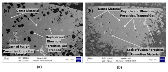
Figure 11.
SEM images of AM 99.9% silver samples at 30 μm layer thickness with a scan speed and hatch distance of (a) 800 mm/s and 0.14 mm, and (b) 600 mm/s and 0.15 mm, Reprinted with permission from ref. [27]. 2020 Elsevier.
The effect of L-PBF process variables for producing Ag jewelry on the material microstructure was discussed by Korium et al. [28]. A silver ring obtained by L-PBF is represented in Figure 12. Ring support structure characteristics and proper geometry were established. The microstructures of silver samples had internal porosities and defects with a laser power of 50 W [28,29], achieving a relative density of 91.06%. Additionally, optimal process parameters are further required to fabricate the dense part with a reduction in porosity and other defects [30].
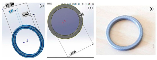
Figure 12.
CAD geometry of the Ag ring (a,b) and the product obtained by L-PBF (c), used under CC BY 4.0 [28].
2.2.3. AM of Platinum Material
Additive manufacturing of platinum presents several challenges due to its unique material properties, which require precise control of laser process parameters to avoid defects such as porosity and cracks. Yadroitsava et al. explored the use of L-PBF for processing pure platinum with optimized laser power (300 W), scan speed (800 mm/s), and layer thickness (30 µm) to produce platinum parts with densities up to 99.98% and minimal porosity. However, achieving fine, uniform grain structures necessary for high-quality platinum parts demands a delicate balance between build speed and part quality. The high thermal conductivity can lead to rapid heat dissipation, making it difficult to maintain the melt pool stability and achieve uniform layer fusion [31]. Figure 13 shows a platinum ring with a defective surface in the right-side ring shank due to an irregular melt and unsupported structure. This defective surface was analyzed by SEM (Figure 14), which shows a highly porous surface due to the balling effect of the melt pool and the adhesion of the powder particles (Figure 15). Klotz et al. fabricated a platinum ring with high relative density (99.8%) with the optimized process parameters of 500 mm/s as the scanning speed, 63 µm of hatch distance, and 95 W of laser power (using a Nd:YAG laser with a spot size of 30 µm and a wavelength of 1064 nm) [32].
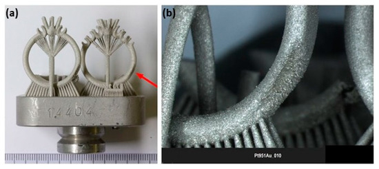
Figure 13.
(a) Additive manufacturing of platinum ring; (b) defects of the ring shank on one side, Reprinted from ref. [32].
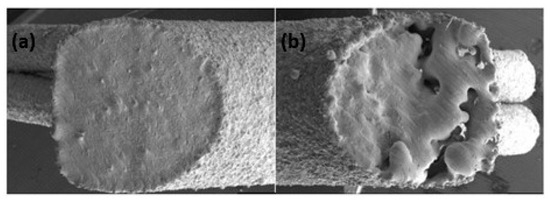
Figure 14.
SEM image of the left side (a) and right side (b) of the ring shank surface (red color arrow in Figure 13a), Reprinted from ref. [32].
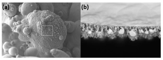
Figure 15.
SEM images of the right ring shank surface area (a,b), Reprinted from ref. [32].
Vorobyev and Guo [33] investigated femtosecond laser processing of platinum to address some of these difficulties. The study demonstrated that femtosecond laser blackening significantly enhanced absorptance, achieving about 95% over a broad wavelength range (250–2500 nm). Despite these advancements, maintaining high absorptance and reducing reflectance (below 5%) across such a wide spectrum involves meticulous control over the laser parameters and processing environment. Blackened platinum surfaces were produced without chemical changes, underscoring the importance of physical modifications to overcome the material’s natural reflectivity [33].
2.2.4. AM of Pure Copper Material
The fabrication of pure copper via laser-based additive manufacturing has huge challenges due to the high reflectivity, high thermal conductivity, low laser absorption, high electrical conductivity, and oxidation sensitivity of copper with the 1070 nm wavelength infrared laser (Figure 16a) [34,35]. Due to the low absorption behavior of pure copper, the fabricated parts, in general, exhibit various defects such as low density, high porosity, balling effect, layer delamination, and crack formation (Figure 16c–f) [36,37]. Also, the high reflectivity of copper substrate can lead to damage in the optical mirror [38], as shown in Figure 16b [39,40]. The high reflectivity and thermal conductivity of copper require the use of higher levels of laser power and careful control of process parameters to achieve the desired material properties. A bi-directional scanning strategy with a 90° rotation between subsequent layers, using a laser power of 725 W and a scan speed of 400 mm/s, can be preferably used; however, despite these efforts, achieving uniform and fully dense parts was challenging due to the inherent properties of copper [41].
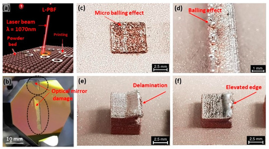
Figure 16.
(a) L-PBF with 1070 nm wavelength, Reprinted from ref. [34], (b) damage of the optical mirror due to laser back reflection from the copper substrate and specific defects, Reprinted with permission from ref. [36], 2019 Elsevier (c) micro-balling effect, Reprinted from ref. [38], (d) balling effect, Reprinted from ref. [38], (e) delamination, Reprinted from ref. [38], (f) elevated edge, Reprinted from ref. [38].
For example, a relative density of 99% was achieved with a laser power of 500 W and a volumetric energy density range of 230–350 J/mm3. The L-PBF fabricated parts demonstrated tensile properties with a yield strength of 122 ± 1 MPa, an ultimate strength of 211 ± 4 MPa, and an elongation of 43 ± 3% [42]. Further, the densification and the thermal and electrical conductivity of the parts were enhanced by high laser power [43,44]. In the future, copper jewelry could be printed using non-thermal AM techniques such as cold spray additive manufacturing. This technique is similar to the traditional powder metallurgy route, though it lacks the flexibility and customization capabilities provided by other 3D printing methods [45].
2.3. Strategies to Improve the L-PBF Processability of Precious Metals
Although laser additive manufacturing technology has considerable advantages, there are some problems that need to be eliminated. As already reported, the high reflectivity of materials such as gold, silver, platinum, and copper means that a significant portion of the laser energy is reflected from the material surface. This reflection reduces the efficiency of the melting process, making it difficult to achieve the desired density and uniformity in the fabricated parts. High reflectivity can also damage the laser optical system, further complicating the manufacturing process. This low absorption rate requires the use of higher laser power, which can increase the risk of thermal distortion and residual stresses in the final product.
The methods suggested in the bibliography to overcome these problems are covered below. These methods involve the use of various alloying elements, powder coating, or the use of low wavelength lasers to enhance the metal absorbance. Alloying elements like gallium, germanium, and silicon can reduce reflectivity and improve laser absorption, leading to better fusion and reduced porosity. Powder coating can further enhance laser energy absorption and melting efficiency. Low-wavelength lasers (i.e., green or blue lasers) provide higher absorptivity, enabling the fabrication of high-quality components with improved mechanical properties (Figure 17).
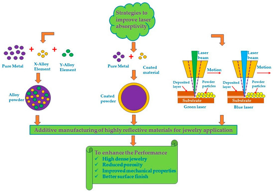
Figure 17.
Schematic representation of a strategy to improve the laser absorptivity in additive manufacturing processes for jewelry application.
2.3.1. Dopant Addition Strategy
The state of the art in the selection and analysis of the influence of doping of precious materials is illustrated in the following sections, broken down by the type of base metal.
Gold-Based Alloys
L-PBF of gold alloys has made significant advancements in achieving higher densification, reduced porosity, improved mechanical properties, and enhanced hardness. These improvements are largely attributed to the careful selection and incorporation of alloying elements, which increase the absorptivity of gold (Figure 18).
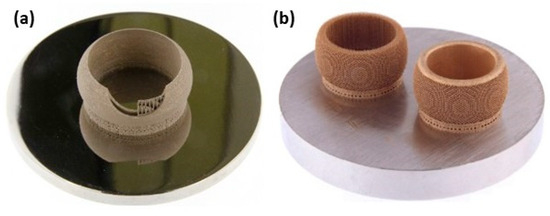
Figure 18.
L-PBF of Au alloys: (a) white-gold and (b) red gold, Reprinted from ref. [25].
Zito et al. reported several innovative materials that can be used to create a wide range of jewelry pieces (Table 1). An element that can increase the gold absorption, i.e., is gallium. The authors reported two different gold alloy powders (Au:Ag:Cu:Ga = 18.8:1:5.2:0 and Au:Ag:Cu:Ga = 37.6:2:9.4:1) successfully manufactured using L-PBF. The addition of gallium resulted in low surface tension, which plays a key role in achieving the proper wettability for better adhesion between the deposition layers to produce defect-free AM components [46]. The improvement of surface quality and the reduction of porosity was also obtained by the addition of Ge and Si (Table 1). Figure 19 shows the gold alloy ring fabricated by L-PBF with two different set of parameters (standard and optimized) which differ mainly for the overlapping rate. Due to the higher laser overlapping rate, the jewelry fabricated with the optimized parameters (65 W, 330 mm/s, layer thickness 20 μm, and 75% of overlapping) ensured high densification with less defects and higher resolution with respect to the standard one (76.2 W, 250 mm/s, layer thickness 30 μm, 50% of overlapping). Moreover, the use of finer particle sizes (<15 μm) allowed for obtaining higher resolutions and smoother surfaces of the jewelry parts (Figure 20) [47].
Figure 19.
Gold alloy ring obtained by (a) standard (76.2 W, 250 mm/s, layer thickness 30 μm, 50% of overlapping) and (b) optimized parameters (65 W, 330 mm/s, layer thickness 20 μm, and 75% of overlapping); (c–f) SEM images of pave obtained using the two sets of parameter, Reprinted from ref. [47].
Figure 20.
Effect of particle size distribution on the resolution and quality of the obtained surfaces: (a) and (c) PSD < 63 μm; (b) and (d) PSD < 15 μm, Reprinted from ref. [47].
The surface finish plays a key role in jewelry production. D. Zito et al. reported that the surface roughness is reduced from 72 to 55 µm with the addition of germanium in 18 K red gold alloy. Moreover, a better ductility was obtained with the addition of germanium between 0.2 and 0.4 wt%, while above 1.5–2 wt%, the jewelry became unacceptably brittle. In this case, the optimal process parameters for achieving an improved surface finish and reduced porosity are a laser power of 72.5 W, layer thickness of 140 μm, and a scanning speed of 0.33 m/s.
The authors also compared the effect of the addition of niobium and of both niobium and titanium in a gold–silver matrix (Table 1) and observed that almost equivalent hardness and significantly lower density were obtained: approximately 25 and 18% less than an equivalent alloy with palladium and the traditional white gold-nickel alloy [48].
The same authors [49] demonstrated the possibility of increasing the absorption of laser radiation by adding a small concentration of semiconductor elements (Si, Ge) that increase the electrical resistivity and can reduce the thermal conductivity of the red gold alloy, thus improving the L-PBF behavior. The presence of semiconductor elements reduces the porosity and improves the process stability [49,50].
Klotz et al. achieved an improvement in surface quality by optimizing powder composition (Table 1) with Ge, Fe or Ti. Microstructural analysis showed fine grains and low porosity [51] giving the possibility to create intricate and high-end jewelry [52].

Table 1.
Representation of the elemental composition of yellow, red, and white gold (18, 14, 10, and 9 carats) powder alloy by Damiano Zito et al. and U.E. Klotz et al. [47,48,51,53].
Table 1.
Representation of the elemental composition of yellow, red, and white gold (18, 14, 10, and 9 carats) powder alloy by Damiano Zito et al. and U.E. Klotz et al. [47,48,51,53].
| Element Compositions: | Alloy | Gold (Au) wt% | Copper (Cu) wt% | Palladium (Pd) wt% | Nickel (Ni) wt% | Silver (Ag) wt% | Germanium (Ge) wt% | Silicon (Si) wt% | Niobium (Nb) wt% | Zinc (Zn) wt% | Titanium (Ti) wt% | Iron (Fe) wt% | Pd: Ag wt% | Cu: Ni wt% | Cu:Ag wt% |
|---|---|---|---|---|---|---|---|---|---|---|---|---|---|---|---|
| 18 K Yellow gold powder alloy [47,53] | 1 | 75.2 | 12.4 | - | - | 12 | 0.4 | - | - | - | - | - | - | - | 1:1 |
| Gold alloy (Au, Ag, Pd, Cu, Si) [48] | 12 | 76.26 | 13.5 | 1.93 | - | 4.69 | - | 3.62 | - | - | - | - | - | - | - |
| Gold alloy (Au, Nb, Zn) [48] | 13 | 75.2 | - | - | - | - | - | - | 18.5 | 6.3 | - | - | - | - | - |
| Gold alloy (Au, Ag, Ti) [48] | 14 | 75.2 | - | - | - | 8.4 | - | - | - | - | 16.4 | - | - | - | - |
| 3N [51] | 15 | 75.1 | 12.5 | - | - | 12.4 | - | - | - | - | - | - | - | - | - |
| Fe003 [51] | 16 | 75.0 | 13.0 | - | - | 11.3 | - | - | - | - | - | 0.7 | - | - | - |
| Ge001 [51] | 17 | 75.1 | 12.8 | - | - | 11.8 | 0.4 | - | - | - | - | - | - | - | - |
| Ti001 [51] | 18 | 75.2 | 12.8 | - | - | 11.7 | - | - | - | - | 0.3 | - | - | - | - |
| 18 K Red gold powder alloy [53] | 2 | 75.2 | 21 | - | - | 3.6 | 0.2 | - | - | - | - | - | - | - | 5.5:1 |
| 14 K Red gold powder alloy [53] | 3 | 58.7 | 33.45 | - | - | 7.45 | 0.4 | - | - | - | - | - | - | - | 4.5:1 |
| 10 K Red gold powder alloy [53] | 4 | 41.9 | 47.06 | - | - | 10.64 | 0.4 | - | - | - | - | - | - | - | 4.5:1 |
| 9 K Red gold powder alloy [53] | 5 | 37.7 | 50.46 | - | - | 11.44 | 0.4 | - | - | - | - | - | - | - | 4.5:1 |
| 18 K White gold powder alloy [53] | 6 | 72.5 | - | 12.4 | - | 12.2 | 0.2 | - | - | - | - | - | 1:1 | - | - |
| 14 K White gold powder alloy [53] | 7 | 58.5 to 59.5 | - | 15 to 25 | - | 15 to 25 | 0.01 to 1 | - | - | - | - | - | 0.75:1 to 1:0.75 | - | - |
| 10 K White gold powder alloy [53] | 8 | 41.7 to 42.5 | - | 25 to 45 | - | 25 to 45 | 0.01 to 2 | - | - | - | - | - | 0.75:1 to 1:0.75 | - | - |
| 18 K White gold powder alloy [53] | 9 | 72.5 | 17.1 | - | 7.5 | - | 0.2 | - | - | - | - | - | - | 2:1 to 3:1 | - |
| 14 K White gold powder alloy [53] | 10 | 58.5 to 59.5 | 23 to 35 | - | 8 to 20 | - | 0.01 to 1.5 | - | - | - | - | - | - | 2:1 to 3:1 | - |
| 10 K White gold powder alloy [53] | 11 | 41.7 to 42.5 | 35 to 50 | - | 12.5 to 35 | - | 0.01 to 2 | - | - | - | - | - | - | 2:1 to 3:1 | - |
Silver-Based Alloy
The unique properties of silver, such as its high thermal and electrical conductivity with low absorptivity, lead to porous L-PBF components characterized by low mechanical properties. Therefore, the addition of alloying elements, such as Cu and La2O3, to enhance densification, has been widely explored.
The normal sterling silver alloy powder, primarily composed of Ag and Cu, produced unsatisfactory results (Figure 21a) as reported by Fischer-Buehner et al. [22]. Figure 21b–d show similar results for three distinct 925 silver alloy powders, characterized by proprietary additives at the expense of copper. The composition of the additives is not disclosed by the author because the project is still in the research stage. Figure 21e–h display jewelry pieces in 925 Ag, demonstrating that finished surfaces can achieve exceptionally high quality, and are challenging to replicate with even the best casting techniques [22]. The 925 Ag alloy was processed with a laser power of 180 W, a scanning speed of 600 mm/s, a layer thickness of 30 µm, and a hatch spacing of 0.060 mm, reaching a relative density of 96.56% [30]. The microstructure reveals both columnar and elongated grains as shown in Figure 22. Wang et al. and Xiong et al. highlighted that the copper content in 925 silver alloy increased laser absorption, making it easier to process if compared to pure silver [30,54].
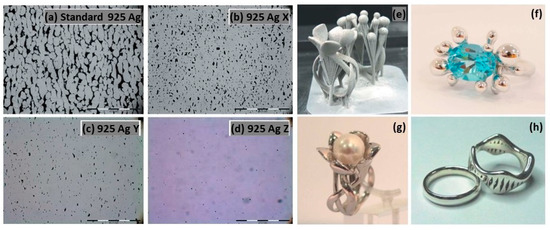
Figure 21.
L-PBF of 925 Ag: (a–d) microstructure investigation with different powder compositions, and (e–h) jewelry parts, Reprinted from ref. [22].
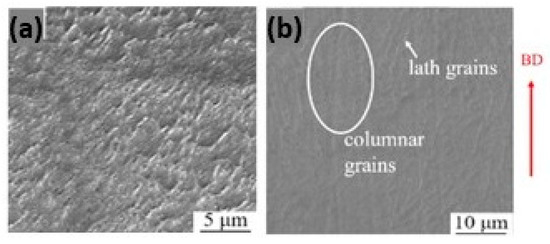
Figure 22.
SEM images of L-PBF (a) Ag and (b) 925 Ag in the build direction (BD), Reprinted from ref. [30].
Zhao et al. [55] explored the addition of La2O3 to Ag–Cu alloys to further enhance their performance. The addition of La2O3 not only enhanced laser absorption but also promoted grain refinement, thereby improving both the mechanical properties and the corrosion resistance of the alloy. In the research, silver with 5.626% of copper was produced by varying the content of La2O3 (0, 0.4, 0.8, and 1.2%). The best results were obtained with 60 W of laser power, a scanning speed of 1000 mm/s, and a layer thickness of 20 µm. The addition of 1.2% of La2O3 resulted in the highest density (9.16 ± 0.55 g/cm3) and significantly improved the mechanical properties, including a nano-indentation hardness of 2.88 GPa with a decrease in porosity as La2O3 was increased (Figure 23a–e) [55].
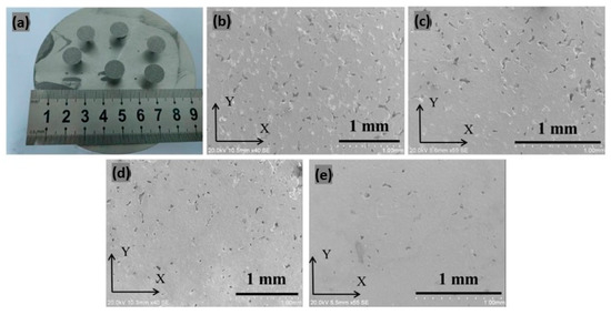
Figure 23.
L-PBF samples of Ag–Cu alloy with different La2O3 content (a) and SEM microstructure obtained on (b) 0, (c) 0.4, (d) 0.8, and (e) 1.2% La2O3 samples, Reprinted from ref. [55].
Platinum-Based Alloy
The addition of semiconductor materials to platinum material significantly enhances their performance in the additive manufacturing process. For example, 800, 850, 900, and 950 Pt alloys were discussed by Corti et al., and the addition of gallium with Pt alloys was studied to enhance the densification and minimize the porosity [56]. Zito et al. investigated a 95PtGaInCu alloy using L-PBF with a 100 W fiber laser, collimated in a 10 µm diameter spot. The optimal processing parameters included a laser power range of 72.5–80 W, a layer thickness of 20 µm, a scanning speed of 0.25 and 0.33 m/s, and a spot distance of 40 µm. The as-built samples exhibited a porosity of 0.06 µm, surface roughness of 40 ± 13 µm, hardness of 222 ± 4 HV, ultimate tensile strength (UTS) of 582 MPa, and elongation of 14.5% [57]. Heat treatment improves hardness and ductility by 16% and 50% as compared to the as-built sample [57].
Figure 24 shows the effect of different element addition on the processability, assessed by single scan tracks (SSTs), of platinum alloy. For example, 2% of Ge has a strong effect with an increase in the track depth; Ga addition, instead, lead to hot cracking. These SSTs indicated that different alloy elements strongly affect processability, emphasizing the importance of optimizing compositions and process parameters.
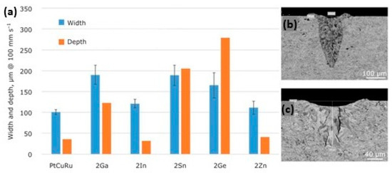
Figure 24.
Influence of the addition of solid suppressing elements in ternary 95Pt-1.5Cu-3.5Ru-X alloys, (X representing gallium, indium, tin, germanium or zinc) (a) and impact of germanium (b) and gallium addition (c) on the SST depth, Reprinted from ref. [32].
Regarding rhodium (PtRh 90-10), it not only increases the material absorption capacity, but also allows for a more uniform and denser microstructure, comparable to conventionally manufactured parts, although the addition of 10% rhodium showed a higher electrical resistivity due to internal vacancies [58]. Wermuth et al. characterized L-PBF samples of platinum rhodium alloy (PtRh 80-20), achieving full density with minimal porosity [59].
Overall, the integration of semiconductor elements like gallium, indium, tin, germanium, zinc or rhodium in platinum alloys significantly improves their performance in additive manufacturing [60]. These enhancements include higher density, reduced porosity, better mechanical properties, and increased suitability for complex geometric designs, making these alloys highly valuable for additive manufacturing in jewelry.
Cu-Based Alloy
Pure copper shows high reflectivity and low absorptivity during the melting process by laser radiation. The high reflectivity represents a high risk due to the increase in the thermal distortion and residual stress of the build components. Therefore, to reduce the reflectivity and increase the absorptivity, copper alloy powders were developed. The addition of pre-alloy powder to pure copper led to reducing the reflectivity from 95 to 55.3% for Cu-15Sn, to 90% for Cu + 2% CNTs (carbon nanotubes), to 32% for Cu + 0.1C and to 44.2% for CuCr0.3 + 0.05C, as shown in Figure 25a–d [61,62,63,64]. Held et al. reported that the addition of tin to copper alloy reduces reflectivity, surface tension, and electrical and thermal conductivity to 80.8%, 1061 mN/m, 12.1% IACS, and 48.5 W/mK. As a result, the porosity decreased, and an enhancement of surface quality can be observed [65].
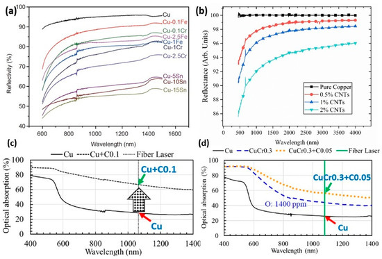
Figure 25.
Comparison of reflectivity of pure copper and its alloy powders: effect of (a) different elements, Reprinted with permission from ref. [61], 2020 Science China Press, different amounts of (b) CNTs, used under CC BY 3.0 [62] (c) C, Reprinted from ref. [63], and (d) Cr and C, Reprinted with permission from ref. [64]. 2019 John Wiley and Sons.
Ayub et al. studied the effect of the addition of different concentrations of CNTs, underlining that CNTs significantly enhance the thermal absorption of copper, allowing for lower laser power levels (<40%), reducing the reflectivity, and enhancing laser absorption. In addition, the densification of the sample with 1.5% CNTs is greater than for pure copper and samples with fewer CNTs, as shown in Figure 26a–d [62].
Figure 26.
SEM micrograph of L-PBF samples of (a) pure copper, (b) Cu-0.5%CNTs, (c) Cu-1%CNTs, and (d) Cu-1.5%CNTs, used under CC BY 3.0 [62].
Jadhav et al. reported that the addition of carbon leads to an in situ deoxidation during the process, although the produced copper samples have a tensile strength of 125 MPa, a ductility of 3%, and an electrical conductivity of 22.7 × 10⁶ S/m, limited by the segregation of carbon nanoparticles and impurities, such as oxygen and phosphorus, at the grain boundaries. Moreover, microstructural analyses showed that defects, such as surface cracks, are primarily owing to the segregation of carbon at the grain boundaries (Figure 27a–d) [63].
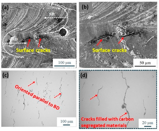
Figure 27.
SEM micrographs of Cu + C0.1 samples. The white arrows in (a) indicate the laser scan direction (b) surface cracks (c) the orientation of the crack parallel to BD (d) cracks filled with carbon segregation, Reprinted from ref. [63].
Jadhav et al. studied the L-PBF behavior of both virgin and carbon-mixed CuCr0.3 powders. Additionally, in this case, carbon nanoparticles facilitate the in situ deoxidation of copper and chromium oxides. The mechanical properties were improved due to the precipitation of nanometric metallic chromium precipitates in the copper matrix (Figure 28c,f). Figure 28a,b show the microstructure of samples with epitaxial columnar grains growth, parallel to the build direction with carbon segregation at the grain boundaries (Figure 28d,e). These results confirm that carbon addition enhances optical absorption without adversely affecting powder properties, and significantly improves mechanical and electrical properties through deoxidation and subsequent precipitation strengthening [64,66].
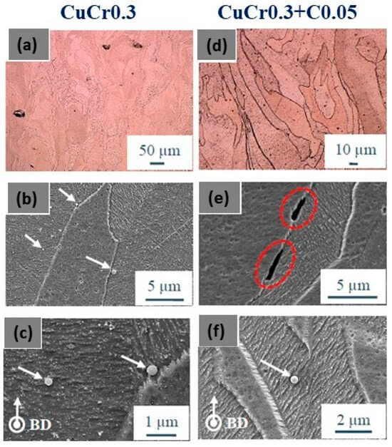
Figure 28.
SEM images of (a–c) Cu alloy and (d–f) CuCr0.3 underlining the epitaxial growth of the columnar grains parallel to the build direction and precipitates and carbon segregation at the grain boundaries, Reprinted with permission from ref. [64]. 2019 John Wiley and Sons.
Robinson et al. studied the effect of the addition of silver on the mechanical and thermal properties of pure copper by L-PBF, observing a significant improvement in mechanical properties [67]. For instance, the CuAg10 alloy, consisting of 92.51% Cu and 7.49% Ag, exhibited a yield strength of 223.5 MPa and an ultimate tensile strength (UTS) of 277.7 MPa. As the silver content increased, the mechanical properties further improved, with CuAg30 (64.20% Cu, 35.80% Ag) showing a yield strength of 330.3 MPa and a UTS of 381.8 MPa [68]. The thermal properties of these alloys were also noteworthy. CuAg alloys maintained high thermal performance with minimal variation despite increasing silver content, showcasing their potential for applications requiring excellent thermal management [68].
In Figure 29a–d, a tin-bronze alloy with a laser power of 95 W, a layer thickness of 20 μm, and varying laser scan speeds from 50 to 400 mm/s was reported. Minimizing the scan speed results in low residual levels of micro-porosity even at the lowest scan speed of 50 mm/s because it greatly enhances the energy available for local melting per volume unit. Instead, decreasing the laser scan speed leads to an increase in processing time and the final L-PBF fabricated product (Figure 29e–h) needs a surface finish post-processing treatment [22].
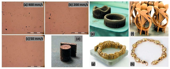
Figure 29.
Effect of scan speed on the microstructure of tin-bronze samples (a–d). Non-optimized (e) and optimized (f) surface roughness in the as-built condition and after surface finishing step (g,h) jewelry parts, Reprinted from ref. [22].
2.3.2. Powder Coating Strategy
A novel approach to overcome the challenges (high reflectivity and thermal conductivity) has been experimented by modifying the powder surface by coating it with less reflective materials. This approach has been used mainly for copper. Coated powders, such as nickel-coated copper powder (Figure 30a–c), have a higher absorption of laser energy (Figure 31a), thus improving the melting efficiency and leading to higher densification and improved mechanical properties. The nickel coating of copper powder particles was achieved by the immersion plating technique. The uncoated copper powder required high energy density from 200 to 500 J/mm3 to melt the powder while the coated powders achieve higher densities with 236 J/mm3 (Figure 32a–d) [69,70,71].
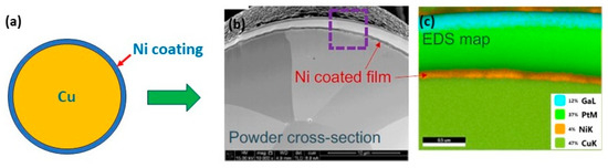
Figure 30.
(a) Schematic representation of Ni-coated copper powders, (b) SEM image, and (c) EDS analysis, Reprinted from refs. [69,70].
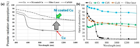
Figure 31.
Optical absorption of pure copper and surface-modified copper powders with different wavelengths. (a) Ni-coated copper powders, Reprinted from refs. [69,70], (b) copper powder treated in a nitrogen environment, Reprinted with permission from ref. [72]. 2020 Elsevier.
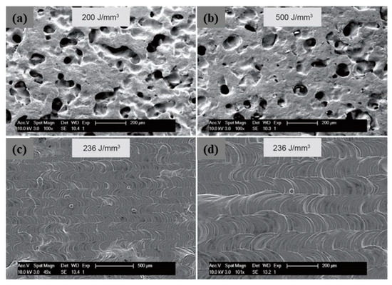
Figure 32.
SEM image of uncoated (a,b) and coated (c,d) Cu samples obtained by L-PBF with different VED, Reprinted from refs. [69,70].
A different approach has been proposed for a CuCr1 powder. The method involves the outward diffusion of chromium in a nitrogen atmosphere, which allows for the formation of a chromium-nitride coating which significantly reduces the optical absorption of the powders (Figure 31b). Moreover, the surface-modified powder exhibited enhanced flowability and minimized oxygen uptake during storage, crucial for maintaining consistent L-PBF performance and part quality. For these reasons, the surface-modified powders have higher densification as compared to unmodified powders (Figure 33a–d) [72].
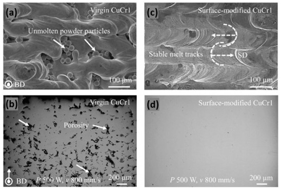
Figure 33.
Optical image of the top surface and cross section of L-PBF produced parts: (a,b) virgin CuCr1; (c,d) surface-modified CuCr1, Reprinted with permission from ref. [72]. 2020 Elsevier.
The highly conductive CuSn0.3 alloy was fabricated via L-PBF using tin-coated copper powder. The copper powder particles were coated with the immersion plating technique that involves a powder pretreatment to remove contaminants (alkaline solution at 80 °C for 5 min) and oxides (0.1 M HCl solution for 1 min), followed by coating and drying. Moreover, the research underlines the detrimental impact of high sulfur content (0.091 wt%) on the L-PBF process, which leads to solidification cracks and porosity, emphasizing the importance of limiting sulfur content to below 0.0025 wt% for optimal results. The coating facilitated the production of crack-free, fully dense copper parts with high thermal conductivity (334 ± 4 W/(m·K)), electrical conductivity (80 ± 1% IACS), tensile strength (256 ± 14 MPa), yield strength (203 ± 4 MPa), and ductility (21 ± 2%) using a fiber laser at 500 W. [73].
Tin and nickel coatings on copper powders for L-PBF was reported by Lindström et al. [74]. The tin and nickel coatings were performed by the immersion deposition method. The coated powders exhibited significantly lower reflectivity (~40%) compared to pure copper (~70%), resulting in lower porosity and better densification (Figure 34) [74].
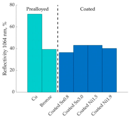
Figure 34.
Comparison of reflectivity behavior of pure and coated copper powders at 1064 nm, Reprinted from ref. [74].
Wadge et al. examined the impact of titanium (Ti) coatings on silver powders to improve absorptivity (from 27% to 45%). A thin and uniform Ti-coating was achieved by physical vapor deposition (pulsed DC magnetron sputtering) optimizing the process parameters (50 W, 3 h). The titanium-coated silver powders demonstrated a significant enhancement over uncoated powders that allow also to reduce the laser power (280 W for coated versus 320 W for uncoated), indicating a more efficient melting process. The enhanced absorptivity facilitated more uniform densification of the powder bed at lower energy densities, resulting in reduced porosity (0.7 ± 1.0% compared to 7.1 ± 2.0% for uncoated powder at 133 J·m−1) [75].
Therefore, the various coated metal powders, including steels, titanium, aluminum, and copper, were examined for their performance in LPBF by Bidulsky et al. The coatings were obtained by several coating methods such as mechanical methods (ball milling, Turbula mixing) and non-mechanical methods (powder immersion, physical vapor deposition, chemical vapor deposition). The mechanical methods are simple and cost-effective but they affect the powder morphology, whereas non-mechanical methods allow one to obtain uniform coatings with methods that are more costly and complex [76]. Finally, titanium diboride (TiB2), aluminum oxide (Al2O3), graphene oxide (GO) and carbon nanotube (CNT) coatings improved hardness, wear resistance, and mechanical properties, achieving relative densities close to the theoretical values [76,77].
To conclude, the use of coated powders in L-PBF processes enhances the absorptivity, flowability, and overall quality of the final parts.
2.3.3. Use of Laser with Lower Wavelength
A very interesting technological approach is to process highly reflective metals using blue laser (wavelength 450 nm, developed by group of researchers led by Prof. Masahiro Tsukamoto at Osaka University’s Joining and Welding Research Institute, in collaboration with Shimadzu Corporation, Nichia Corporation and Furukawa Electric Co., Ltd., in Japan) or green laser (wavelength 515 nm, developed by Fraunhofer Institute of Laser Technology (ILT), Aachen, Germany) characterized by high power and shorter wavelengths than common red lasers. At these wavelengths, in fact, highly reflective materials have a higher absorption of the laser, as shown in Figure 35 [61,78].
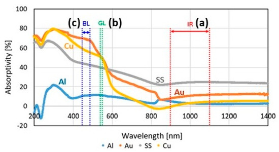
Figure 35.
Laser absorptivity of various high reflective metals from 200 to 1400 nm. The wavelength ranges of (a) IR: infrared laser, (b) GL: green laser, and (c) BL: blue laser are shown, Reprinted from ref. [78].
Green Laser
The use of green lasers, specifically at a wavelength of 515 nm, has been shown to significantly improve the performance of the laser-based additive manufacturing of pure copper with absorption in the range of 40–60% [79,80]. In particular, green lasers reduce reflective losses resulting in parts with better density, lower porosity, improved surface finish, less spatter, and higher productivity (Figure 36) [81]. The pure copper powder, obtained with a green laser, achieved relative densities above 99.95% and electrical conductivity up to 100% IACS, showing superior performance compared to infrared lasers [82,83].
Figure 36.
Comparison of laser-based additive manufacturing of copper cubic structure (four layers) with a green and red laser (laser source: TRUMPF product), Reprinted from ref. [81].
De Terris et al. reported the fabrication of pure copper via L-PBF using both green and infrared laser beams. The green laser, which involves the complete melting of the material, produces superior properties in terms of mechanical, electrical, and thermal performance as compared to the infrared laser. The lack of fusion and keyholes that characterized the microstructure of samples obtained by infrared laser (Figure 37a–c) are completely absent in the samples obtained by the green laser (Figure 37d–f) [84]. The use of a green laser was found to potentially eliminate the need for oxidation or other powder treatments to produce materials with a high thermal conductivity. Porosity was minimized with specific combinations of laser power and scanning speed, achieving a high relative density of up to 99.9% [85,86].
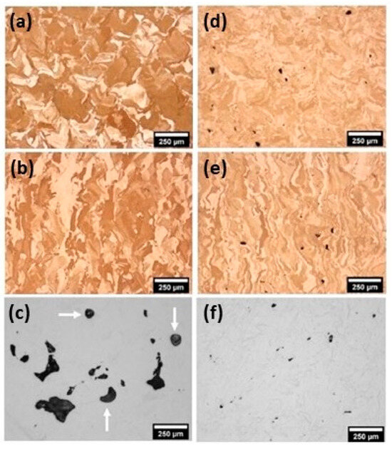
Figure 37.
L-PBF of pure copper: microstructural analysis of samples obtained by (a–c) infrared laser and (d–f) green lasers, Reprinted with permission from ref. [84]. 2023 Springer Nature.
Blue Laser
The application of blue lasers, particularly at a wavelength of 450 nm, has significantly improved the performance of additive manufacturing processes for precious materials due to their high absorptivity (Figure 35c) [78]. Published papers on the use of blue lasers in L-PBF are scarce. Wu et al. reported [87] that the increased absorption allows one to obtain higher densification and reduce the porosity in the final product. The manufactured parts exhibit an almost complete density, up to 99.6%, which enhances the mechanical properties and structural integrity of the material [87]. Other papers were found if weldability is considered. Recently, Pasang et al. further explored the mechanical properties and weldability of pure copper foil using blue diode lasers [75]. Blue diode lasers are absorbed the most (60%), significantly outperforming IR (5%) and green lasers (50%) [88].
Therefore, blue laser processing offers substantial benefits for copper welding and additive manufacturing. The high absorption efficiency of blue lasers at 450 nm leads to better energy utilization and favorable microstructural characteristics [89]. The findings underscore the potential of blue laser technology to overcome the limitations of traditional IR lasers.
2.4. AM of Precious Materials: Conclusion
Additive manufacturing has revolutionized the production of precious metals such as gold, platinum, silver, and copper. It enables intricate designs and complex structures with unprecedented precision. Researchers are actively investigating precious materials with improved properties such as strength, conductivity, and durability through the modification of materials (the addition of specific elements or coatings) and technologies (green or blue lasers). Table 2 provides a summary of the main materials used in the literature for AM jewelry manufacturing, indicating process parameters and obtained properties.
Table 2.
Summary of precious materials used in L-PBF of jewelry applications with process parameters and performance characteristics.
Despite the potential benefits, the proposed methods may face challenges, such as the need for precise control over alloy compositions and coating processes to achieve consistent results. Furthermore, the implementation of low-wavelength lasers may require modifications to existing equipment and processes. Optimizing the parameters for each specific material will be crucial to achieving the desired performance outcomes.
3. Surface Finishing and Post-Processing in Jewelry Fabrication
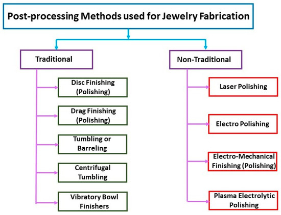
Figure 38.
Post-processing methods used for jewelry fabrication.
AM of precious metal jewelry is gradually gaining ground in the global jewelry business, with many industries already adopting or considering the technology. Two main elements still need to be improved to accelerate technology adoption: (1) AM jewelry design; and (2) AM jewelry polishing and finishing. Fletcher and Cooper analyzed the different polishing and finishing processes for AM precious metal jewelry [94,95,96]. The advantages of the various polishing methods such as Dish Finishing (DIF), Drag Finishing (DF), Stream Finishing (SF), Tumbling or Barreling (TU), Centrifugal Tumbling (CF), Vibratory Bowl Finishers (VBF), Laser Polishing (LP), electrolytic polishing, Electropolishing (EP), Electro-Mechanical Finishing (EMF), and Plasma Electrolytic Polishing (PEP) were discussed. Recent advances have opened up new possibilities for machine-assisted surface treatment techniques, which are becoming increasingly effective. The authors emphasize the many advantages of machine-assisted processing over manual processing, which have contributed greatly to the renaissance of the watch and jewelry industry. Modern finishing technology, in fact, aims to reduce waste, increase value, improve quality and create attractive surfaces, as well as reduce processing times.
For example, several mechanical polishing methods have demonstrated their ability to significantly reduce the time and effort required to achieve an adequate surface finish for an 18-carat AM jewelry article. A comparison of the processing times of various mechanical polishing procedures is illustrated in Figure 39, using hours as the unit of measurement. The reported data indicates that Stream Finishing (SF) is faster than other polishing methods [94].
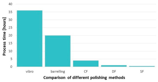
Figure 39.
Time comparison of different polishing processes: Vibratory Bowl Finishers, Barreling, Centrifugal Tumbling (CF), Drag Finishing (DF), and Stream Finishing (SF), Reprinted from ref. [94].
The surface of an L-PBF part consistently shows a rougher texture than that of a cast part, regardless of the adjustments made to the process parameters. Consequently, pre-finishing operations are always necessary before starting regular finishing procedures to ensure that the surfaces achieve the desired smoothness, similar to that of cast parts. This aspect is particularly crucial in the context of surface finishing designs characterized by hollow and perforated structures, such as in the case of bracelets. If L-PBF production were scaled up to production volumes, the problem of as-built surface roughness pre-finishing would have to be addressed, although L-PBF production is currently not considered suitable for mass production, where mass finishing processes are considered essential [22].
Sandblasting, typically considered an exposed process, was able to effectively smooth and brighten L-PBF surfaces, even in the case of complex designs that are usually difficult to access. Figure 40 summarizes the results of the initial experiments on bronze L-PBF parts. Starting with the surface roughness in the state of construction (Figure 40a), dry blasting with corundum sand rapidly polished the surface in 1–2 min (Figure 40b,c); subsequently, a wet micro-sandblasting step with <50 μm glass microspheres further improved the smoothness and brightness in a further one to two minutes (Figure 40d,e). The resulting bronze ring had an excellent surface quality after hand polishing (Figure 40f). In addition, the author used electropolishing to improve gloss in hard-to-reach areas, surpassing traditional finishing techniques [22].
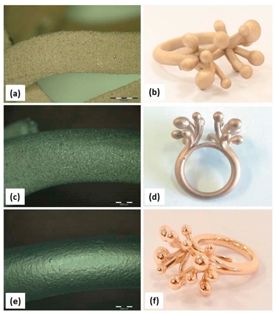
Figure 40.
Post-processing of L-PBF jewelry parts made of tin-bronze alloy. As-built samples (a,b) and after dry (c,d) and wet blasting with corundum (e,f), Reprinted from ref. [22].
Electropolishing, an electrochemical material removal technique mainly used for metal parts, uses an external electric current source. In this process, the material is extracted from the workpiece (anode) and immersed in an electrolyte suited to the chemical composition of the metal, which leads to a significant reduction in surface roughness. The electropolished surface is not affected by the process, resulting in a smooth and highly reflective surface [94].
When metal is subjected to laser polishing, the surface of the metal punctually melts, and the smoothing effect of the liquid phase thus formed is highly dependent on its surface tension. To guide the laser beam, patterns are used that correspond to the contours of the surface. The innovation in laser polishing is rooted in the principle of active remelting, which differs fundamentally from traditional grinding and polishing methods that rely on abrasion and removal. This technique proves effective on hard-to-reach surfaces that are often difficult to clean manually or with machines (Figure 41) [94].
Figure 41.
Laser polishing of a pendant using optimized laser parameters (a,b), Reprinted from ref. [94].
In electromechanical polishing, the metal object is coated with a gel-like substance and immersed in an appropriate electrolyte solution. During polishing, the microscopic particles of the gel are brushed against the metal surface, making it possible to treat articulated parts such as necklaces or interior walls inaccessible by mechanical means (Figure 42). Electroplasma polishing is a new surface treatment that produces exceptionally smooth and highly polished surfaces. Although PEP is considered an electropolishing process, it uses environmentally friendly, non-acidic electrolytes and operates at relatively high temperatures and voltages to achieve a better surface finish [94].
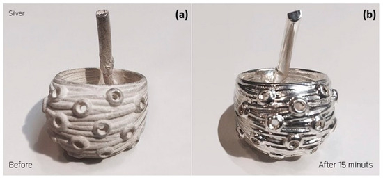
Figure 42.
Electro-mechanical polished sample (a) before and (b) after a 15-min treatment, Reprinted from ref. [94].
The application of mechanical polishing to additive manufacturing (AM) jewelry has proven effective in reducing manual finishing and polishing activities [94]. Ready-to-sell surfaces have been created by mass-finishing machines (MFM). Even though these MFMs use the prescribed finishing medium, it is often possible to improve the results by making some minor modifications to process variables such as speed, duration, compound, etc. The process parameters of the mass finishing machine to achieve better results have been evaluated and modified by Moser [97]. Overall, the polishing sequence, such as sandblasting, electropolishing, and hand polishing, is necessary to achieve a better surface finish (Figure 43a–c).
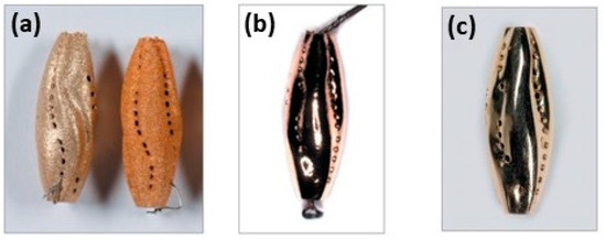
Figure 43.
Surface polishing of yellow-gold jewelry followed by various steps: (a) sandblasted, (b) electro-polished, and (c) hand-polished, Reprinted from ref. [23].
In summary, despite these advances, further research is needed to identify the most suitable mechanical finishing process that offers an optimal reduction in processing time. It is important to note that many of these processes are still at an early commercialization or experimental stage. Furthermore, extensive investigation and testing are required before incorporating them into the jewelry industry.
Table 3.
Post-processing of AM for jewelry application.
Table 3.
Post-processing of AM for jewelry application.
| Fabrication Method | Post-Processing Technique | Principle | Material Used | Feature Size (µm) | Advantage | Disadvantage |
|---|---|---|---|---|---|---|
| Traditional | Disc polishing [94,95,97] | Material is removed and smoothed from the workpiece surface using rotating and an abrasive slurry. | Abrasive materials are alumina, silicon carbide and diamond were used | 0.1–1.0 | High-quality surface finish, Mirror finish surface, Adaptability, Suitable for complex features | Time-consuming process for larger components, larger waste generation, and multiple steps were required |
| Drag Polishing [94,95] | Utilizes a revolving drag plate and abrasive slurry to polish and sculpt the surface of a workpiece. | Diamond was used as an abrasive material and water as a carrier fluid | 0.05–0.5 | Precise and surface finish and material removal, efficient for intricate shape and adaptable for several materials | Knowledgeable operators are required, Limited to specific geometries, and produce a waste slurry. | |
| Tumbling or barreling [94] | Surface polishing is accomplished by friction and impact in a spinning barrel or drum packed with abrasive material. | Various materials, such as steel pins, ceramic beads, or abrasive stones, were used as abrasive media. | 5–50 | Efficient for edge radiusing, polishing and deburring, mainly utilized for batch production | It may take more stages to achieve a mirror-like quality, making it unsuitable for highly delicate or detailed components. | |
| Centrifugal Tumbling [94] | It uses a fast-revolving drum or bowl to polish surfaces by contacting them at high speeds while exposing workpieces and abrasive material to centrifugal forces. | Abrasive media such as steel, plastic and ceramic were used | 1–20 | Surface finishing that is effective and reliable, suitable for deburring, polishing, and edge radii, and ideal for different materials. | Better options for delicate or detailed components may exist, batch processing is only possible, and appropriate medium and compound selection is needed. | |
| Vibratory Bowl Finishers (VBF) [94,95] | It uses a vibratory bowl to transfer vibrational energy to combine workpieces, abrasive media, and a liquid compound, aiding surface finishing by relative motion and friction. | Abrasive media such as steel, plastic and ceramic were used | 1–30 | Deburring, polishing, and surface refinement techniques that are successful in batch processing, suited for various materials, and suitable for a wide range of materials. | It needs careful medium and compound selection, may not be the best option for highly delicate or detailed pieces, and makes noise while in use. | |
| Non-Traditional | Laser Polishing (LP) [94] | Utilizes a powerful laser beam to melt and re-solidify the material’s surface, producing a polished and smooth finish. | No abrasive materials used (Laser beams), depends on the laser absorption and interaction properties. | 0.01–0.1 | Minimum material removal, provides precise control and the capacity to focus on specific areas, producing high quality finishes. | Limited to certain materials, it could be needed for post-processing processes and might be sluggish for larger components. |
| Electro polishing (EP) [94] | The controlled removal of a layer of material from a metal’s surface using an electrolytic bath and an electric current to produce a polished and smooth finish. | Electrolytes used (for example, sulfuric acid, phosphoric acid) | 0.1–10 | Enhances corrosion resistance, offers a high-quality, mirror-like surface, and reaches intricate details and complicated geometries. | Limited to metals, could need specialist equipment, and the procedure can be relatively slow for larger components. | |
| Electro- mechanical polishing [94,98] | Combines mechanical and electrochemical abrasion to remove material from the workpiece’s surface, improving flatness and quality. | Combination of electrolytes and abrasives (For example, electrolytic solutions and diamond paste) | 0.05–1.0 | Produces surfaces with an optimal flatness and smoothness, appropriate for the manufacturing of semiconductors, and is highly automatable. | Limited to certain materials and applications, can be sluggish for larger components, and may need specialist equipment. | |
| Plasma Electrolytic polishing (PEP) [94] | Polish and remove material from a metal’s surface using a mix of electrolytic action and plasma discharge to produce a smooth and polished finish. | Electrolytic solutions (For example, alkaline solutions) | 0.1–10 | Provides a mirror-like polish, improves surface cleanliness, and increases corrosion resistance; it is suited for many metal alloys. | Restricted to metals, it may demand specialized machinery and can be mostly sluggish for large components. |
4. Future Directions of Additive Manufacturing for Jewelry Industries
Although many jewelry industries still use traditional methods to produce jewelry with huge, attractive parts [99], in recent times, the jewelry industry has been impacted by the additive manufacturing technique and research is still ongoing to produce high-quality jewelry parts with cost-effective methods. Initially, additive manufacturing was integrated with traditional craftsmanship (Figure 44). Integration has improved the design and post-processing of jewelry products, such as surface finishing, stone setting, and assembly, which are related to quality assurance [100,101].
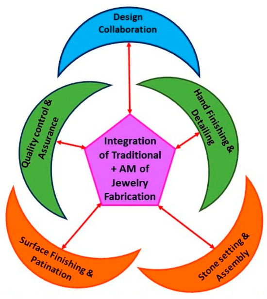
Figure 44.
AM of jewelry production and integration with TM.
Integrating additive manufacturing technologies into the jewelry industry involves several challenges. The transition from traditional methods to AM requires significant changes in workflow, which often meet with resistance from skilled craftsmen. The initial investment in AM equipment and staff training is considerable, especially for smaller companies, and difficult to justify without immediate returns. In addition, ensuring consistent quality and expanding the range of suitable materials, particularly precious metals, remains an ongoing problem that requires robust quality control and further research [100].
Despite significant advancements, additive manufacturing technologies are still maturing and facing significant research gaps and challenges. The process variables in the AM process, such as laser power, scanning speed, hatching distance, layer thickness, etc., are not yet fully understood, which affects product quality and consistency. The lack of standardized processes and materials leads to production inconsistencies, highlighting the necessity of establishing industry standards. Additionally, extensive post-processing is often required, emphasizing the need for research to streamline these steps. Studies on the long-term durability of AM-produced jewelry under everyday wear are also essential. Finally, developing hybrid manufacturing approaches that integrate AM with traditional techniques is crucial for leveraging the strengths of both methods [101].
In particular, digital design of jewelry parts will improve the jewelry industry productivity and design freedom to realize complex structures with greater precision.
In order for craft enterprises to adapt to technological developments, the following three strategic directions need to be pursued: (1) embracing the use of digital technologies rather than seeing technology as a threat to the enterprise’s future, (2) involving customers in the design and production processes and expanding the enterprise’s network, and (3) offering craft products through a wide range of services. The following strategic paths will help craft enterprises to survive, innovate, and increase their competitive advantage by exploiting the possibilities offered by innovative technologies and new production methods [102,103].
On the other hand, however, there are still many challenges to be faced when considering the future direction of the jewelry industry, particularly with regard to material choice, design complexity, surface finish, production speed, and efficiency (Figure 45). Moreover, the future perspective of additive manufacturing of jewelry will focus on the introduction of different types of innovative alloys, hybrid AM (manufacturing with post-processing), real-time monitoring, machine learning (ML), deep learning (DL) and Internet of Things (IoT) to improve the accuracy of jewelry pieces.
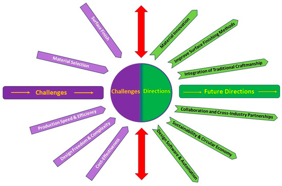
Figure 45.
Future perspective of jewelry and furniture production by AM.
As far as materials are concerned, some jewelry applications still require more consumer-friendly alloys, such as harder alloys with higher tarnish resistance. Further research is needed to determine whether new alloys, such as shape memory alloys and bulk metallic glasses, are usable. Furthermore, with regard to nickel in white golds and cadmium in welds, future health and safety regulations may impose further restrictions on alloy compositions and encourage their further development [104]. Finally, the addition of semiconductor materials in precious metals and composite materials, such as precious metal matrix composites (PMMCs), could be explored in the future [104].
Next, the automation of additive manufacturing with post-processing (surface finishing) needs to be evaluated in order to increase the productivity of jewelry products that can become cost-effective (Industry 5.0). Real-time monitoring systems for additive manufacturing can enable the automatic identification of defects on the line and in situ, saving time and material [105]. The use of, among other things, machine vision to assess the quality of a 3D print [106,107] can make processes more efficient and reduce scrap [108,109,110]. For example, IoT closely monitors the scanning process, providing recommendations for optimal scanning for superior results. This integration addresses challenges related to material parameters, surface topology, data integration, and communication between scanning and additive manufacturing devices. Actuators, sensors, and other IoT connectivity devices play a crucial role in improving coordination between these devices. In addition, the use of artificial intelligence (AI) for 3D scanning is envisioned, foreseeing a future where the process is as simple as shooting a movie with a smartphone [111,112].
5. Conclusions
This article represents a comprehensive review on the use of AM for jewelry making. Nowadays, jewelry design has received new life through the incorporation of AM. As personal adornment is redefined through the lens of technology, this synergy goes beyond mere aesthetics. Using additive techniques (such as L-PBF), objects are created with precious materials such as gold, silver, and platinum. The main challenge in fabricating precious materials with L-PBF is their low absorbency and high thermal conductivity. This paper explores potential solutions to overcome these problems and improve the properties of precious materials produced by L-PBF. In addition, post-processing techniques improve surface finish and reduce porosity. Each piece of jewelry represents creativity and craftsmanship, allowing for the tangible manifestation of one’s unique talent. In addition to simplifying production, this combination of technology and craftsmanship ushers in a new era of cutting-edge jewelry that combines tradition and innovation. From the literature review, the following observations emerged:
- L-PBF is a good alternative for producing high-quality jewelry because of its superior mechanical strength, accuracy, and surface finish quality compared to powder metallurgy processes.
- Enhancing material-use efficiency in L-PBF for jewelry is essential for overcoming challenges like oxidation, agglomeration, and contamination. This can be achieved by better handling sensitive powders and optimizing recycling processes, thereby improving the sustainability and cost-effectiveness of this advanced manufacturing (L-PBF) method than the traditional method.
- This review highlights various strategies to optimize the performance of precious jewelry materials in L-PBF. In particular:
- The addition of alloying elements to precious materials can significantly increase mechanical strength, thermal stability, and overall durability by improving absorption at the common laser wavelength.
- Powder coating in precious metal fabrication using L-PBF improves laser absorption and reduces defects, resulting in higher densification and better surface quality. This approach is particularly beneficial for intricate jewelry designs, providing superior surface finish and structural integrity.
- The use of low-wavelength lasers (green or blue lasers) can be a technological approach to improve the properties of precious metals fabricated by L-PBF. These lasers improve energy absorption and reduce thermal gradients, leading to higher material density and reduced porosity.
- LP excels over other surface polishing techniques in producing accurate surface qualities, making it an excellent choice for high-end jewelry with complex patterns that require precise surface finishes.
- The integration of AM with traditional craftsmanship in jewelry production improves design flexibility, quality control, customization, and efficiency.
Author Contributions
Conceptualization, G.T., E.P. and F.B.; methodology, G.T. and M.L.; software, G.T.; validation, G.T., E.P. and F.B.; formal analysis, G.T., S.F., S.B., D.U. and P.F.; investigation, G.T.; resources, P.F. and F.B.; data curation, G.T.; writing—original draft preparation, G.T., S.F. and E.P.; writing—review and editing, G.T., E.P., S.B., M.L., D.U., P.F. and F.B.; visualization, G.T. and D.U.; supervision, F.B.; project administration, E.P. and F.B.; funding acquisition, M.L. and F.B. All authors have read and agreed to the published version of the manuscript.
Funding
This study was carried out within the MICS (Made in Italy—Circular and Sustainable) Extended Partnership and received funding from the European Union Next-GenerationEU (PIANO NAZIONALE DI RIPRESA E RESILIENZA (PNRR)—MISSIONE 4 COMPONENTE 2, INVESTIMENTO 1.3—D.D. 1551.11-10-2022, PE00000004). This manuscript reflects only the authors’ views and opinions, neither the European Union nor the European Commission can be considered responsible for them.
Data Availability Statement
No new data were created or analyzed in this study. Data sharing is not applicable to this article.
Acknowledgments
All authors thank the initiative PNRR Partenariato Esteso for providing funding to Politecnico Di Torino under MICS “Circular & Sustainable Made in Italy”—PE00000004—CUP E13C22001900001. Also, I would like to express my gratitude to all the authors whose work I referenced and who have made significant contributions to this field.
Conflicts of Interest
The authors declare no conflicts of interest.
References
- Attaran, M. The Rise of 3-D Printing: The Advantages of Additive Manufacturing over Traditional Manufacturing. Bus. Horiz. 2017, 60, 677–688. [Google Scholar] [CrossRef]
- Kumar, R.; Kumar, M.; Singh Chohan, J. Material-Specific Properties and Applications of Additive Manufacturing Techniques: A Comprehensive Review. Bull. Mater. Sci. 2021, 44, 181. [Google Scholar] [CrossRef]
- ISO/ASTM 52900:2021(E); Additive Manufacturing-General Principles-Fundamentals and Vocabulary. ISO/ASTM: Geneva, Switzerland; West Conshohocken, PA, USA, 2021.
- Bhuvanesh Kumar, M.; Sathiya, P. Methods and Materials for Additive Manufacturing: A Critical Review on Advancements and Challenges. Thin Walled Struct. 2021, 159, 107228. [Google Scholar] [CrossRef]
- Pratheesh Kumar, S.; Elangovan, S.; Mohanraj, R.; Ramakrishna, J.R. Review on the Evolution and Technology of State-of-the-Art Metal Additive Manufacturing Processes. In Materials Today: Proceedings; Elsevier Ltd.: Amsterdam, The Netherlands, 2021; Volume 46, pp. 7907–7920. [Google Scholar]
- Srivastava, M.; Rathee, S.; Patel, V.; Kumar, A.; Koppad, P.G. A Review of Various Materials for Additive Manufacturing: Recent Trends and Processing Issues. J. Mater. Res. Technol. 2022, 21, 2612–2641. [Google Scholar] [CrossRef]
- Parupelli, S.K.; Desai, S. A Comprehensive Review of Additive Manufacturing (3D Printing): Processes, Applications and Future Potential. Am. J. Appl. Sci. 2019, 16, 244–272. [Google Scholar] [CrossRef]
- Cooper, F. Sintering and Additive Manufacturing: The New Paradigm for the Jewellery Manufacturer. Johns. Matthey Technol. Rev. 2015, 59, 233–242. [Google Scholar] [CrossRef]
- Yap, Y.L.; Yeong, W.Y. Additive Manufacture of Fashion and Jewellery Products: A Mini Review: This Paper Provides an Insight into the Future of 3D Printing Industries for Fashion and Jewellery Products. Virtual Phys. Prototyp. 2014, 9, 195–201. [Google Scholar] [CrossRef]
- Cooper, F. Sintering and Additive Manufacturing: “Additive Manufacturing and the New Paradigm for the Jewellery Manufacturer”. Progress. Addit. Manuf. 2016, 1, 29–43. [Google Scholar] [CrossRef]
- Ferreira, T.; Almeida, H.A.; Bártolo, P.J.; Campbell, I. Additive Manufacturing in Jewellery Design. In Proceedings of the ASME 2012 11th Biennial Conference on Engineering Systems Design and Analysis, Nantes, France, 2–4 July 2012; pp. 187–194. [Google Scholar]
- Ferreira, T.; Almeida, H.A.; Campbell, I.; Bartolo, P.J. Additive Manufacturing and Design Strategies for Customized Jewellery Production. In Proceedings of the International Conference on Competitive Manufacturing, Sellenbosch, South Africa, 30 January–1 February 2013; pp. 1–7. [Google Scholar]
- Cooper, F. DMLM Support: Are They the Jewelry Industry’s New Sprue, Riser and Gate Feed. In The Santa Fe Symposium on Jewelry Technology; Santa Fe Symposium: Albuquerque, NM, USA, 2014; pp. 1–22. [Google Scholar]
- Li, X.G.; Zhu, Q.; Shu, S.; Fan, J.Z.; Zhang, S.M. Fine Spherical Powder Production during Gas Atomization of Pressurized Melts through Melt Nozzles with a Small Inner Diameter. Powder Technol. 2019, 356, 759–768. [Google Scholar] [CrossRef]
- Ünal, R.; Aydın, M. High Efficient Metal Powder Production by Gas Atomisation Process. Mater. Sci. Forum 2007, 534–536, 57–60. [Google Scholar] [CrossRef]
- Strauss, J.T. Powder Metallurgy (P/M) Applications in Jewelry Manufacturing. In The Santa Fe Symposium on Jewelry Manufacturing Technology; Santa Fe Symposium: Albuquerque, NM, USA, 1997; pp. 105–131. [Google Scholar]
- Strauss, J.T. P/M (Powder Metallurgy) and Potential Applications in Jewelry Manufacturing. In The Santa Fe Symposium on Jewelry Manufacturing Technology; Santa Fe Symposium: Albuquerque, NM, USA, 1998; pp. 389–433. [Google Scholar]
- Raw, P.M. Mass Production of Gold and Platinum Wedding Rings Using Powder Metallurgy. In The Santa Fe Symposium on Jewelry Manufacturing Technology; Santa Fe Symposium: Albuquerque, NM, USA, 2000; pp. 251–270. [Google Scholar]
- Strauss, J.T. Powder Metallurgy In Jewelry Manufacturing: Status Report and Discussion. In The Santa Fe Symposium on Jewelry Manufacturing Technology; Santa Fe Symposium: Albuquerque, NM, USA, 2008; pp. 295–306. [Google Scholar]
- Tunick Strauss, J.; Strauss, J.T. P/M (Powder Metallurgy) in Jewelry Manufacturing; Current Status, New Developments, and Future Projections. In The Santa Fe Symposium on Jewelry Manufacturing Technology; Santa Fe Symposium: Albuquerque, NM, USA, 2003; pp. 387–412. [Google Scholar]
- Wiesner, K.; Gold, C.H. Sintering Technology for Jewelry and Multicolor Rings Sintering Technology for Jewellery and Multicolour Rings. In Proceedings of the 19th Santa Fe Symposium on Jewellery Manufacturing Technology, Albuquerque, NM, USA, 22–25 May 2005; Gold Bulletin. pp. 188–193. [Google Scholar]
- Fischer-Buehner, J.; Poliero, P.; Bertoncello, R.; Basso, A.; Poliero, M.; Group, L. Rapid Jewelry Manufacturing by Laser Melting of Precious Metal Powders (PLM): Fiction or Future? In The Santa Fe Symposium on Jewelry Manufacturing Technology; Santa Fe Symposium: Albuquerque, NM, USA, 2012; pp. 177–202. [Google Scholar]
- Klotz, U.E.; Tiberto, D.; Held, F. Additive Manufacturing of 18-Karat Yellow-Gold Alloys. In The Santa Fe Symposium on Jewelry Manufacturing Technology; Santa Fe Symposium: Albuquerque, NM, USA, 2016; pp. 255–272. [Google Scholar]
- Khan, M.; Dickens, P. Selective Laser Melting (SLM) of Pure Gold. Gold Bull. 2010, 43, 114–121. [Google Scholar] [CrossRef]
- Zito, D.; Allodi, V.; Sbornicchia, P.; Rappo, S.; Trissino, P.S.P.A. Why Should We Direct 3D Print Jewelry? A Comparison between Two Thoughts: Today and Tomorrow. In The Santa Fe Symposium on Jewelry Manufacturing Technology; Santa Fe Symposium: Albuquerque, NM, USA, 2017; pp. 515–556. [Google Scholar]
- Damiano Zito, B.; Carlotto, A.; Loggi, A.; Bortolamei, S.; Zito, D.; Alberto Molinari, I.; Cristofolini, I. Latest Developments in Selective Laser Melting Production of Gold Jewelry. In The Santa Fe Symposium on Jewelry Manufacturing Technology 2012; Santa Fe Symposium: Albuquerque, NM, USA, 2012; pp. 537–562. [Google Scholar]
- Robinson, J.; Stanford, M.; Arjunan, A. Stable Formation of Powder Bed Laser Fused 99.9% Silver. Mater. Today Commun. 2020, 24, 101195. [Google Scholar] [CrossRef]
- Korium, M.S.; Roozbahani, H.; Alizadeh, M.; Perepelkina, S.; Handroos, H. Direct Metal Laser Sintering of Precious Metals for Jewelry Applications: Process Parameter Selection and Microstructure Analysis. IEEE Access 2021, 9, 126530–126540. [Google Scholar] [CrossRef]
- Robinson, J.; Stanford, M.; Arjunan, A. Correlation between Selective Laser Melting Parameters, Pore Defects and Tensile Properties of 99.9% Silver. Mater. Today Commun. 2020, 25, 101550. [Google Scholar] [CrossRef]
- Wang, D.; Wei, Y.; Wei, X.; Khanlari, K.; Wang, Z.; Feng, Y.; Yang, X. Selective Laser Melting of Pure Ag and 925Ag Alloy and Their Thermal Conductivity. Crystals 2022, 12, 480. [Google Scholar] [CrossRef]
- Yadroitsava, I.; Yadroitsev, I.; Zyl, I. Van Laser Based Powder Bed Fusion of Pure Platinum. In Proceedings of the International Conference on Competitive Manufacturing (COMA 19), Stellenbosch, South Africa, 30 January–1 February 2019; pp. 188–193. [Google Scholar]
- Klotz, U.E.; König, F.R. Additive Manufacturing of Platinum Alloys. Johns. Matthey Technol. Rev. 2023, 67, 303–316. [Google Scholar] [CrossRef]
- Vorobyev, A.Y.; Guo, C. Femtosecond Laser Blackening of Platinum. J. Appl. Phys. 2008, 104, 053516. [Google Scholar] [CrossRef]
- Zhu, Y.Q.; Yang, Y.Q.; Wang, D.; Chen, F.; Deng, C.; Chen, X.J. Progress in Laser Melting Technology of Pure Copper/Copper Alloy Highly Reflective Material Powder Bed. J. Mater. Eng. Cailiao Gongcheng 2022, 50, 1–11. [Google Scholar]
- Colopi, M.; Demir, A.G.; Caprio, L.; Previtali, B. Limits and Solutions in Processing Pure Cu via Selective Laser Melting Using a High-Power Single-Mode Fiber Laser. Int. J. Adv. Manuf. Technol. 2019, 104, 2473–2486. [Google Scholar] [CrossRef]
- Stoll, T.; Trautnitz, P.; Schmiedeke, S.; Franke, J.E.; Travitzky, N. Process Development for Laser Powder Bed Fusion of Pure Copper. In Proceedings of the Laser 3D Manufacturing VII, San Francisco, CA, USA, 4–6 February 2020; SPIE–International Society for Optics and Photonics: Bellingham, WA, USA, 2020; pp. 24–38. [Google Scholar]
- Bojestig, E.; Cao, Y.; Nyborg, L. Surface Chemical Analysis of Copper Powder Used in Additive Manufacturing. Surf. Interface Anal. 2020, 52, 1104–1110. [Google Scholar] [CrossRef]
- Jadhav, S.D.; Dadbakhsh, S.; Goossens, L.; Kruth, J.P.; Van Humbeeck, J.; Vanmeensel, K. Influence of Selective Laser Melting Process Parameters on Texture Evolution in Pure Copper. J. Mater. Process Technol. 2019, 270, 47–58. [Google Scholar] [CrossRef]
- Jiang, Q.; Zhang, P.; Yu, Z.; Shi, H.; Wu, D.; Yan, H.; Ye, X.; Lu, Q.; Tian, Y. A Review on Additive Manufacturing of Pure Copper. Coatings 2021, 11, 740. [Google Scholar] [CrossRef]
- Roccetti Campagnoli, M.; Galati, M.; Saboori, A. On the Processability of Copper Components via Powder-Based Additive Manufacturing Processes: Potentials, Challenges and Feasible Solutions. J. Manuf. Process 2021, 72, 320–337. [Google Scholar] [CrossRef]
- Sinico, M.; Cogo, G.; Benettoni, M.; Calliari, I.; Pepato, A. Influence of Powder Particle Size Distribution on the Printability of Pure Copper for Selective Laser Melting. In Proceedings of the 30th Annual International Solid Freeform Fabrication Symposium—An Additive Manufacturing Conference, Austin, TX, USA, 12–14 August 2019; pp. 657–667. [Google Scholar]
- Jadhav, S.D.; Goossens, L.R.; Kinds, Y.; Hooreweder, B.V.; Vanmeensel, K. Laser-Based Powder Bed Fusion Additive Manufacturing of Pure Copper. Addit. Manuf. 2021, 42, 101990. [Google Scholar] [CrossRef]
- Kaden, L.; Matthäus, G.; Ramm, R.; Ullsperger, T.; Seyfarth, B.; Nolte, S. Additive Manufacturing of Pure Copper Using Ultrashort Laser Pulses. In Proceedings of the Laser 3D Manufacturing VI, San Francisco, CA, USA, 5–7 February 2019; SPIE–International Society for Optics and Photonics: Bellingham, WA, USA, 2019; pp. 49–55. [Google Scholar]
- Kromer, R.; Gorny, C.; Gruhier, E.; Le Guen, E.; Arvieu, C.; Lacoste, E. Absorptivity Measurement of Solid and Powder Bed under IR Laser Beam. Opt. Laser Technol. 2023, 157, 108508. [Google Scholar] [CrossRef]
- Hutasoit, N.; Rashid, R.A.R.; Palanisamy, S.; Duguid, A. Effect of Build Orientation and Post-Build Heat Treatment on the Mechanical Properties of Cold Spray Additively Manufactured Copper Parts. Int. J. Adv. Manuf. Technol. 2020, 110, 2341–2357. [Google Scholar] [CrossRef]
- Zito, D.; Carlotto, A.; Loggi, A.; Sbornicchia, P.; Maggian, D.; Progold, S.A.; Vi, T.; Fockele, M.; Unterberg, P. Optimisation of the Main Selective Laser Melting Technology Parameters in the Production of Gold Jewellery Authors. Int. J. Powder Metall. 2015, 51, 43. [Google Scholar]
- Zito, D.; Saccardo, E.; Sbornicchia, P.; Allodi, V.; Cepeda, G.A.; Progold, A. Innovative Printing Strategy for High-Resolution Jewelry Production by Selective Laser Melting. In The Santa Fe Symposium on Jewelry Manufacturing Technology; Santa Fe Symposium: Albuquerque, NM, USA, 2022; pp. 629–666. [Google Scholar]
- Zito, D.; Allodia, V.; Sbornicchia, P.; Rappo, S.; Fiorese, L. Direct 3D Metal Printing: A Trip through New Opportunities and Innovative Alloys. In The Santa Fe Symposium on Jewelry Manufacturing Technology; Santa Fe Symposium: Albuquerque, NM, USA, 2017; pp. 473–514. [Google Scholar]
- Carlotto, A.; Loggi, A.; Sbornicchia, P.; Zito, D.; Maggian, D.; Molinari, A.; Cristofolini, I. Optimization of SLM Technology Main Parameters in the Production of Gold and Platinum Jewelry. In The Santa Fe Symposium on Jewelry Manufacturing Technology; Santa Fe Symposium: Albuquerque, NM, USA, 2014; pp. 439–470. [Google Scholar]
- Zito, D.; Carlotto, A.; Loggi, A.; Sbornicchia, P.; Bruttomesso, D.; Rappo, S. Definition and Solidity of Gold and Platinum Jewelry Produced Using Selective Laser Melting (SLMTM) Technology. In The Santa Fe Symposium on Jewelry Manufacturing Technology; Santa Fe Symposium: Albuquerque, NM, USA, 2015; pp. 455–492. [Google Scholar]
- Klotz, U.E.; Tiberto, D.; Held, F. Optimization of 18-Karat Yellow Gold Alloys for the Additive Manufacturing of Jewelry and Watch Parts. Gold. Bull. 2017, 50, 111–121. [Google Scholar] [CrossRef]
- Jhabvala, J.; Boillat, E.; Glardon, R. On the Use of EBSD Analysis to Investigate the Microstructure of Gold Samples Built by Selective Laser Melting. Gold. Bull. 2011, 44, 113–118. [Google Scholar] [CrossRef][Green Version]
- Zito, D. Use of Gold Powder Alloys for Manufacturing Jewellery Items by Selective Laser Melting. 2015, pp. 1–22. Available online: https://patents.justia.com/patent/20170164700 (accessed on 5 May 2020).
- Xiong, W.; Hao, L.; Peijs, T.; Yan, C.; Cheng, K.; Gong, P.; Cui, Q.; Tang, D.; Al Islam, S.; Li, Y. Simultaneous Strength and Ductility Enhancements of High Thermal Conductive Ag7.5Cu Alloy by Selective Laser Melting. Sci. Rep. 2022, 12, 4250. [Google Scholar] [CrossRef]
- Zhao, X.; Zheng, H.; Ma, X.; Sheng, Y.; Zeng, D.; Yuan, J. Microstructure, Mechanical Properties, and Corrosion Resistance of Ag–Cu Alloys with La2O3 Fabricated by Selective Laser Melting. Materials 2023, 16, 7670. [Google Scholar] [CrossRef]
- Corti, C.W. The Evolution of Platinum Jewellery Alloys: From the 1920s to the 2020s: Developments in New Alloys and Techniques. Johns. Matthey Technol. Rev. 2022, 66, 418–434. [Google Scholar] [CrossRef]
- Zito, D.; Allodi, V.; Trevisan, F.; Rossini, M.G.M.; Rossini, A.; Mazza, M. Potential and innovation of selective laser melting technique in platinum jewelry production. In The Santa Fe Symposium on Jewelry Manufacturing Technology; Santa Fe Symposium: Albuquerque, NM, USA, 2018; pp. 625–684. [Google Scholar]
- Becker, T.; Gries, T. Properties of Additively Manufactured Platinum-Rhodium Alloys. Johns. Matthey Technol. Rev. 2023, 67, 266–277. [Google Scholar] [CrossRef]
- Wermuth, L.; Beyer, S.; Sebald, T.; Schütze, M.; Deck, J.; Riß, F.; Humm, S.; Koch, M. Characterization of Platinum Alloy Powder-PtRh 80-20-for Additive Layer Manufacturing. In Proceedings of the 6th European Conference for Aeronautics and Space Sciences (EUCASS), Krakow, Poland, 29 June–3 July 2015; Volume 1, pp. 1–11. [Google Scholar]
- Laag, T.; Heinrich, J. Advantages and Challenges of Platinum Group Metals Powder Processing. In The 2018 Santa Fe Symposium on Jewelry Manufacturing Technology; Santa Fe Symposium: Albuquerque, NM, USA, 2018; pp. 327–343. [Google Scholar]
- Gu, R.N.; Wong, K.S.; Yan, M. Laser Additive Manufacturing of Typical Highly Reflective Materials-Gold, Silver and Copper. Sci. Sin. Phys. Mech. Astron. 2020, 50, 034204. [Google Scholar] [CrossRef]
- Ayub, H.; Khan, L.A.; McCarthy, E.; Ahad, I.U.; Sreenilayam, S.P.; Fleischer, K.; Brabazon, D. Optical Absorption and Conduction of Copper Carbon Nanotube Composite for Additive Manufacturing. In Materials Research Proceedings; Association of American Publishers: Washington, DC, USA, 2023; Volume 28, pp. 111–118. [Google Scholar]
- Jadhav, S.D.; Dadbakhsh, S.; Vleugels, J.; Hofkens, J.; Puyvelde, P.V.; Yang, S.; Kruth, J.P.; Van Humbeeck, J.; Vanmeensel, K. Influence of Carbon Nanoparticle Addition (and Impurities) on Selective Laser Melting of Pure Copper. Materials 2019, 12, 2469. [Google Scholar] [CrossRef] [PubMed]
- Suraj Dinkar Jadhav, I.; Dadbakhsh, S.; Rong Chen, I.; Shabadi, R.; Kruth, J.-P.; Van Humbeeck, J.; Vanmeensel, K. Modification of Electrical and Mechanical Properties of Selective Laser-Melted CuCr0.3 Alloy Using Carbon Nanoparticles. Adv. Eng. Mater. 2020, 22, 1900946. [Google Scholar] [CrossRef]
- Held, F.; Klotz, U.E. Effect of Material Properties and Process Parameters in Powder Bed Additive Manufacturing; Santa Fe Symposium: Albuquerque, NM, USA, 2022. [Google Scholar]
- Jadhav, S.D.; Dhekne, P.P.; Brodu, E.; Van Hooreweder, B.; Dadbakhsh, S.; Kruth, J.P.; Van Humbeeck, J.; Vanmeensel, K. Laser Powder Bed Fusion Additive Manufacturing of Highly Conductive Parts Made of Optically Absorptive Carburized CuCr1 Powder. Mater. Des. 2021, 198, 109369. [Google Scholar] [CrossRef]
- Robinson, J.; Arjunan, A.; Baroutaji, A.; Stanford, M. Mechanical and Thermal Performance of Additively Manufactured Copper, Silver and Copper–Silver Alloys. Proc. Inst. Mech. Eng. Part L J. Mater. Des. Appl. 2021. [Google Scholar] [CrossRef]
- Robinson, J.; Arjunan, A.; Stanford, M.; Lyall, I.; Williams, C. Effect of Silver Addition in Copper-Silver Alloys Fabricated by Laser Powder Bed Fusion in Situ Alloying. J. Alloys Compd. 2021, 857, 157561. [Google Scholar] [CrossRef]
- Jadhav, S.D.; Dadbakhsh, S.; Kruth, J.-P.; Humbeeck, J.V.; Vanmeensel, K. SLM of Copper and Copper Based Alloys. In Proceedings of the Arenberg Youngster Seminar 16, 2018, Leuven, Belgium, 16 October 2018. [Google Scholar]
- Suraj Dinkar, J.; Vanmeensel, K. Laser-Based Powder Bed Fusion Additive Manufacturing of Highly Conductive Copper and Copper Alloys; KU Leuven: Leuven, Belgium, 2021. [Google Scholar]
- Jadhav, S.D. Selective Laser Melting of Copper and Copper Alloys: Issues and Remedies. In Proceedings of the 9th International Conference on’Additive Manufacturing Technologies-AM 2019, Bengaluru, India, 6–7 September 2019. [Google Scholar]
- Jadhav, S.D.; Dhekne, P.P.; Dadbakhsh, S.; Kruth, J.P.; Van Humbeeck, J.; Vanmeensel, K. Surface Modified Copper Alloy Powder for Reliable Laser-Based Additive Manufacturing. Addit. Manuf. 2020, 35, 101418. [Google Scholar] [CrossRef]
- Jadhav, S.D.; Fu, D.; Deprez, M.; Ramharter, K.; Willems, D.; Van Hooreweder, B.; Vanmeensel, K. Highly Conductive and Strong CuSn0.3 Alloy Processed via Laser Powder Bed Fusion Starting from a Tin-Coated Copper Powder. Addit. Manuf. 2020, 36, 101607. [Google Scholar] [CrossRef]
- Lindström, V.; Liashenko, O.; Zweiacker, K.; Derevianko, S.; Morozovych, V.; Lyashenko, Y.; Leinenbach, C. Laser Powder Bed Fusion of Metal Coated Copper Powders. Materials 2020, 13, 3493. [Google Scholar] [CrossRef]
- Wadge, M.D.; Lowther, M.; Cooper, T.P.; Reynolds, W.J.; Speidel, A.; Carter, L.N.; Rabbitt, D.; Kudrynskyi, Z.R.; Felfel, R.M.; Ahmed, I.; et al. Tailoring Absorptivity of Highly Reflective Ag Powders by Pulsed-Direct Current Magnetron Sputtering for Additive Manufacturing Processes. J. Mater. Process Technol. 2023, 317, 117985. [Google Scholar] [CrossRef]
- Bidulsky, R.; Gobber, F.S.; Bidulska, J.; Ceroni, M.; Kvackaj, T.; Grande, M.A. Coated Metal Powders for Laser Powder Bed Fusion (L-PBF) Processing: A Review. Metals 2021, 11, 1831. [Google Scholar] [CrossRef]
- Tidén, S.; Diaz, L.C.; Taher, M.; Jansson, U. Synthesis of Graphene Oxide Coated Metal Powders with Improved Flowability and Reduced Reflectance. Surf. Coat. Technol. 2022, 444, 128644. [Google Scholar] [CrossRef]
- Pasang, T.; Fujio, S.; Lin, P.C.; Tao, Y.; Sudo, M.; Kuendig, T.; Sato, Y.; Tsukamoto, M. Weldability and Mechanical Properties of Pure Copper Foils Welded by Blue Diode Laser. Materials 2024, 17, 2140. [Google Scholar] [CrossRef]
- Nordet, G.; Gorny, C.; Mayi, Y.; Daligault, J.; Dal, M.; Effernelli, A.; Blanchet, E.; Coste, F.; Peyre, P. Absorptivity Measurements during Laser Powder Bed Fusion of Pure Copper with a 1 KW Cw Green Laser. Opt. Laser Technol. 2022, 147, 107612. [Google Scholar] [CrossRef]
- Lu, P.; Cheng-Lin, Z.; Tong, L.; Xin-Yu, L.; Jiang-Lin, L.; Shun, L.; Wen-Hao, W.; Heng-Hua, Z. Molten Pool Structure and Temperature Flow Behavior of Green-Laser Powder Bed Fusion Pure Copper. Mater. Res. Express 2022, 9, 016504. [Google Scholar] [CrossRef]
- Fu, E.; Spiegelhalder, R.; Vogt, S.; Goebel, M. The Best Kept Secret in Laser Additive Manufacturing: Green Lasers, a Unique Innovation. In Proceedings of the Laser 3D Manufacturing IX, San Francisco, CA, USA, 22–27 January 2022; SPIE–International Society for Optics and Photonics: Bellingham, WA, USA, 2022; pp. 1–6. [Google Scholar]
- Gruber, S.; Stepien, L.; López, E.; Brueckner, F.; Leyens, C. Physical and Geometrical Properties of Additively Manufactured Pure Copper Samples Using a Green Laser Source. Materials 2021, 14, 3642. [Google Scholar] [CrossRef]
- Johnson, K.; Burden, E.; Shaffer, M.; Noack, T.; Mueller, M.; Walker, J.; MacDonald, E.; Cortes, P.; Quintana, J. A Copper Pyramidal Fractal Antenna Fabricated with Green-Laser Powder Bed Fusion. Progress. Addit. Manuf. 2022, 7, 931–942. [Google Scholar] [CrossRef]
- De Terris, T.; Baffie, T.; Ribière, C. Additive Manufacturing of Pure Copper: A Review and Comparison of Physical, Microstructural, and Mechanical Properties of Samples Manufactured with Laser-Powder Bed Fusion (L-PBF), Electron Beam Melting (EBM) and Metal Fused Deposition Modelling (MFDM) Technologies. Int. J. Mater. Form. 2023, 16, 32. [Google Scholar] [CrossRef]
- Domine, A.; Verdy, C.; Penaud, C.; Vitu, L.; Fenineche, N.; Dembinski, L. Selective Laser Melting (SLM) of Pure Copper Using 515-Nm Green Laser: From Single Track Analysis to Mechanical and Electrical Characterization. Int. J. Adv. Manuf. Technol. 2023, 127, 3723–3741. [Google Scholar] [CrossRef]
- Alphonso, W.E.; Bayat, M.; Hattel, J. Comparison between green and infrared laser in laser powder bed fusion of pure copper through high fidelity numerical modelling at meso-scale. In Mathematical Modelling of Weld Phenomena 13; Institute of Materials Science, Joining and Forming: Graz, Austria, 2022; pp. 21–39. [Google Scholar] [CrossRef]
- Wu, D.; Sun, J.; Li, Z.; Tashiro, S.; Murphy, A.B.; Ma, N.; Tanaka, M.; Huang, J.; Feng, K.; Liu, C.; et al. Dynamic Vapor and Keyhole Behavior, and Equiaxed Dendrite Formation in Blue Laser Processing of Copper. Int. J. Heat. Mass. Transf. 2023, 209, 124102. [Google Scholar] [CrossRef]
- Liu, X.; Wang, H.; Kaufmann, K.; Vecchio, K. Directed Energy Deposition of Pure Copper Using Blue Laser. J. Manuf. Process 2023, 85, 314–322. [Google Scholar] [CrossRef]
- Zediker, M.S.; Silva Sa, M.J.; Finuf, M.; Fritz, R.; Tucker, J.; Pelaprat, J.M. Blue Laser Diode (450 Nm) System for Welding Copper. In Proceedings of the High-Power Diode Laser Technology XVI, San Francisco, CA, USA, 19 February 2018; SPIE–International Society for Optics and Photonics: Bellingham, WA, USA; pp. 1–8. [Google Scholar]
- Abdelhafiz, M.; Al-Rubaie, K.S.; Emadi, A.; Elbestawi, M.A. Process–Structure–Property Relationships of Copper Parts Manufactured by Laser Powder Bed Fusion. Materials 2021, 14, 2945. [Google Scholar] [CrossRef] [PubMed]
- Jadhav, S.D.; Vleugels, J.; Kruth, J.P.; Van Humbeeck, J.; Vanmeensel, K. Mechanical and Electrical Properties of Selective Laser-Melted Parts Produced from Surface-Oxidized Copper Powder. Mater. Des. Process. Commun. 2020, 2, e94. [Google Scholar] [CrossRef]
- Sinico, M.; Jadhav, S.D.; Witvrouw, A.; Vanmeensel, K.; Dewulf, W. A Micro-Computed Tomography Comparison of the Porosity in Additively Fabricated Cucr1 Alloy Parts Using Virgin and Surface-Modified Powders. Materials 2021, 14, 1995. [Google Scholar] [CrossRef] [PubMed]
- Wang, D.; Li, K.; Yao, J.; Du, B.; Xu, Y. Porosity, Texture, and Mechanical Properties of Pure Copper Fabricated by Fine Green. Laser Powder Bed Fusion. SSRN 2024, 1–22. [Google Scholar] [CrossRef]
- Fletcher, D. The Precious Project: Polishing and Finishing of Additive Manufacturing (AM) Jewelry. 2018. Available online: https://www.santafesymposium.org/2018-santa-fe-symposium-papers/2018-precious-project-polishing-and-finishing-additive-manufacturing-am-jewelry (accessed on 31 May 2018).
- Moser Martin Polishing up on Finishing or How to Stay Competitive due to Optimized Surface Finishing. In The Santa Fe Symposium on Jewelry Manufacturing Technology; Santa Fe Symposium: Albuquerque, NM, USA, 2001; pp. 305–329.
- Klaus Wiesner, B.; Schmidtke, M.; Ernst Vetter, E.; Wiesner Wieland, K.; Schmidtke Ernst, M. Some Basic Aspects of Manual Polishing with Rotating Instruments. In Proceedings of the 23rd Santa Fe Symposium on Jewelry Manufacturing Technology, Albuquerque, NM, USA, 17–20 May 2009; Santa Fe Symposium: Albuquerque, NM, USA, 2009; pp. 377–389. [Google Scholar]
- Moser, M. How to Get That “Ready to Sell” Finish from Your Disc-Finishing Machine. In The Santa Fe Symposium on Jewelry Manufacturing Technology; Santa Fe Symposium: Albuquerque, NM, USA, 2003; pp. 267–288. [Google Scholar]
- Verdooren, A.; Albuquerque, G. Advantages and Limitations of Electro-Mechanical Finishing. In Proceedings of the 23rd Santa Fe Symposium on Jewelry Manufacturing Technology; Santa Fe Symposium: Albuquerque, NM, USA, 2009; pp. 417–433. [Google Scholar]
- Nagulpelli, K.S.; King, R.E.; Warsing, D. Integrated Traditional and Additive Manufacturing Production Profitability Model. Procedia Manuf. 2019, 34, 619–630. [Google Scholar] [CrossRef]
- Jacobs, J.; Zoran, A. Hybrid Practice in the Kalahari: Design Collaboration through Digital Tools and Hunter-Gatherer Craft. In Proceedings of the Conference on Human Factors in Computing Systems–Proceedings 18–23 April 2015, San Francisco, CA, USA; Association for Computing Machinery: New York, NY, USA, 2015; Volume 15, pp. 619–628. [Google Scholar]
- Stamati, V.; Antonopoulos, G.; Azariadis, P.; Fudos, I. A Parametric Feature-Based Approach to Reconstructing Traditional Filigree Jewelry. CAD Comput. Aided Des. 2011, 43, 1814–1828. [Google Scholar] [CrossRef]
- Bertacchini, F.; Bilotta, E.; Demarco, F.; Pantano, P.; Scuro, C. Multi-Objective Optimization and Rapid Prototyping for Jewelry Industry: Methodologies and Case Studies. Int. J. Adv. Manuf. Technol. 2021, 112, 2943–2959. [Google Scholar] [CrossRef]
- Bonfanti, A.; Del Giudice, M.; Papa, A. Italian Craft Firms Between Digital Manufacturing, Open Innovation, and Servitization. J. Knowl. Econ. 2018, 9, 136–149. [Google Scholar] [CrossRef]
- Corti, C.W. Jewelry Alloys-Past, Present and Future. In Proceedings of the Goldsmiths’ Company Jewellery Materials Congress, London, UK, 8–9 July 2019; pp. 1–24. [Google Scholar]
- Liu, T.; Huang, L.; Chen, B. Real-Time Defect Detection of Laser Additive Manufacturing Based on Support Vector Machine. In Journal of Physics: Conference Series; Institute of Physics Publishing: Bristol, UK, 2019; Volume 1213. [Google Scholar]
- Paraskevoudis, K.; Karayannis, P.; Koumoulos, E.P. Real-Time 3D Printing Remote Defect Detection (Stringing) with Computer Vision and Artificial Intelligence. Processes 2020, 8, 1464. [Google Scholar] [CrossRef]
- Li, Y.; Polden, J.; Pan, Z.; Cui, J.; Xia, C.; He, F.; Mu, H.; Li, H.; Wang, L. A Defect Detection System for Wire Arc Additive Manufacturing Using Incremental Learning. J. Ind. Inf. Integr. 2022, 27, 100291. [Google Scholar] [CrossRef]
- Vu, V.Q.; Tran, M.Q.; Vu, L.T. Editorial: Applications of Artificial Intelligence and IoT Technologies in Smart Manufacturing. Front. Mech. Eng. 2023, 9, 110804. [Google Scholar] [CrossRef]
- Li, R.; Jin, M.; Paquit, V.C. Geometrical Defect Detection for Additive Manufacturing with Machine Learning Models. Mater. Des. 2021, 206, 109726. [Google Scholar] [CrossRef]
- Gawade, V.; Singh, V.; Guo, W. “Grace” Leveraging Simulated and Empirical Data-Driven Insight to Supervised-Learning for Porosity Prediction in Laser Metal Deposition. J. Manuf. Syst. 2022, 62, 875–885. [Google Scholar] [CrossRef]
- Chigilipalli, B.K.; Karri, T.; Chetti, S.N.; Bhiogade, G.; Kottala, R.K.; Cheepu, M. A Review on Recent Trends and Applications of IoT in Additive Manufacturing. Appl. Syst. Innov. 2023, 6, 50. [Google Scholar] [CrossRef]
- Nasiri, S.; Khosravani, M.R. Machine Learning in Predicting Mechanical Behavior of Additively Manufactured Parts. J. Mater. Res. Technol. 2021, 14, 1137–1153. [Google Scholar] [CrossRef]


Disclaimer/Publisher’s Note: The statements, opinions and data contained in all publications are solely those of the individual author(s) and contributor(s) and not of MDPI and/or the editor(s). MDPI and/or the editor(s) disclaim responsibility for any injury to people or property resulting from any ideas, methods, instructions or products referred to in the content. |
© 2024 by the authors. Licensee MDPI, Basel, Switzerland. This article is an open access article distributed under the terms and conditions of the Creative Commons Attribution (CC BY) license (https://creativecommons.org/licenses/by/4.0/).