Crystal Structures of GaN Nanodots by Nitrogen Plasma Treatment on Ga Metal Droplets


Abstract
:1. Introduction
2. Materials and Methods
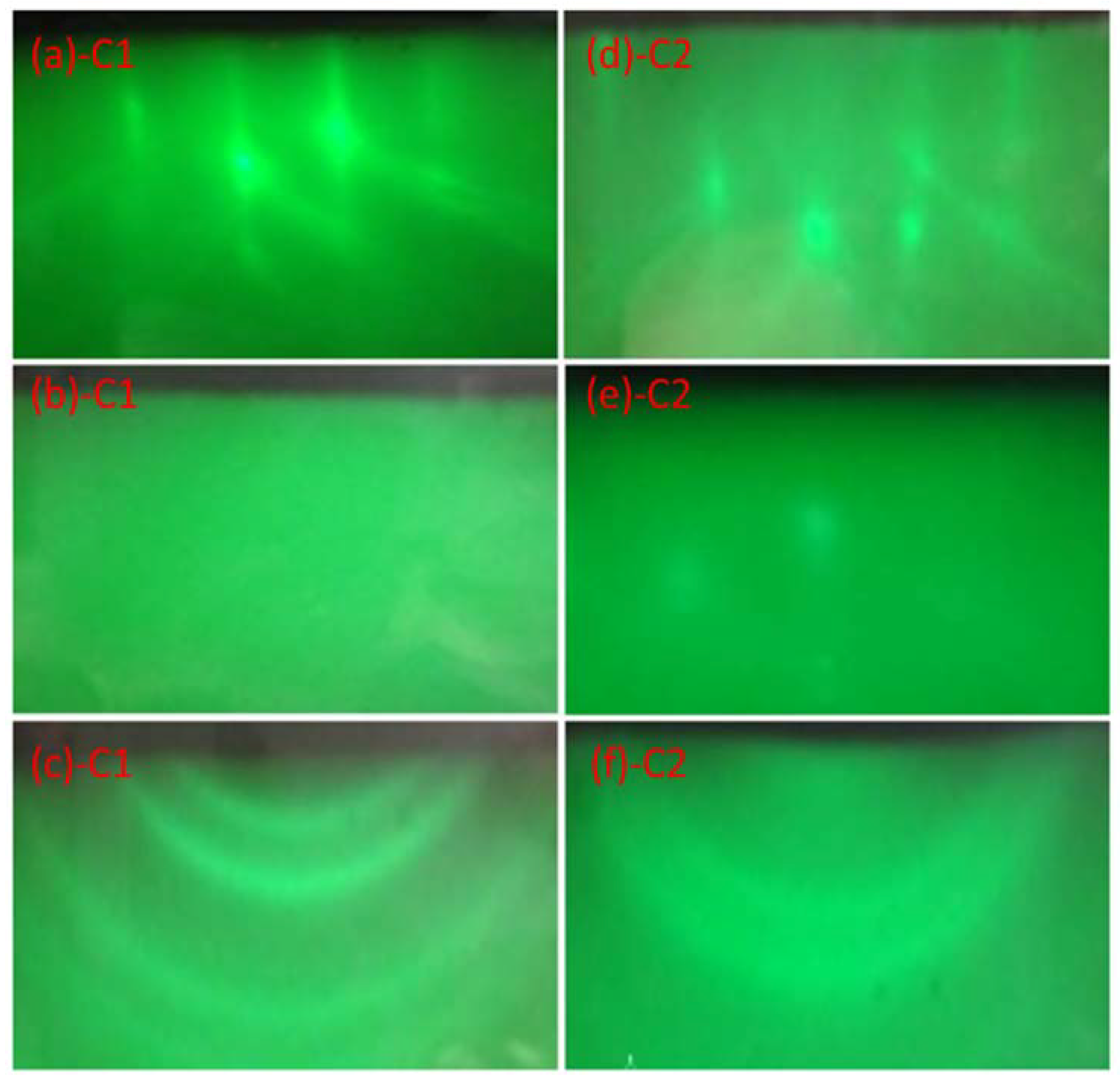
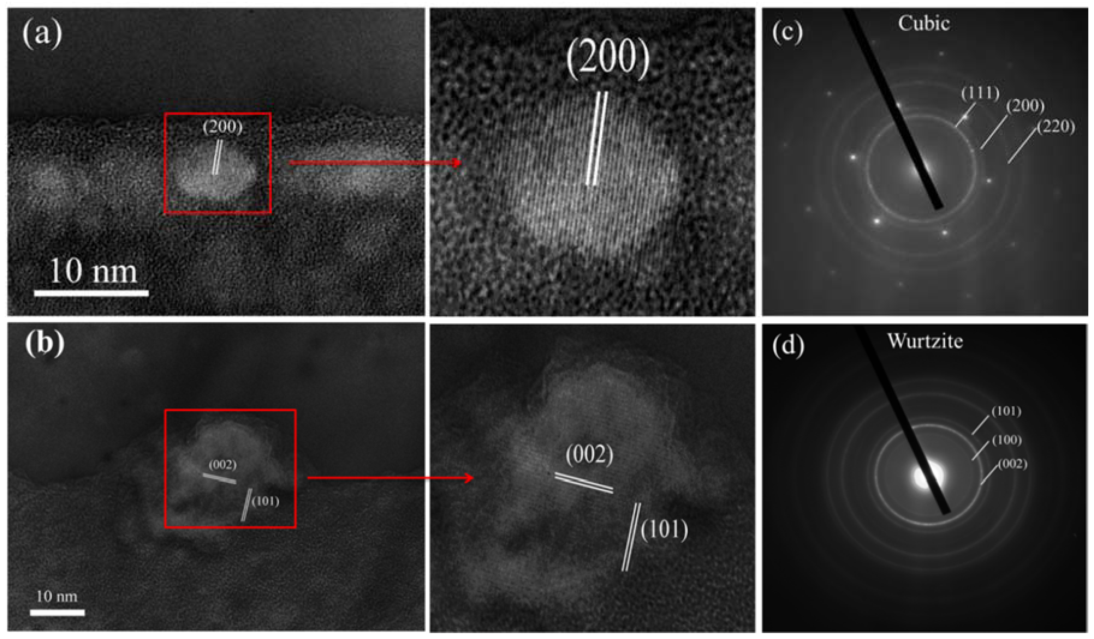
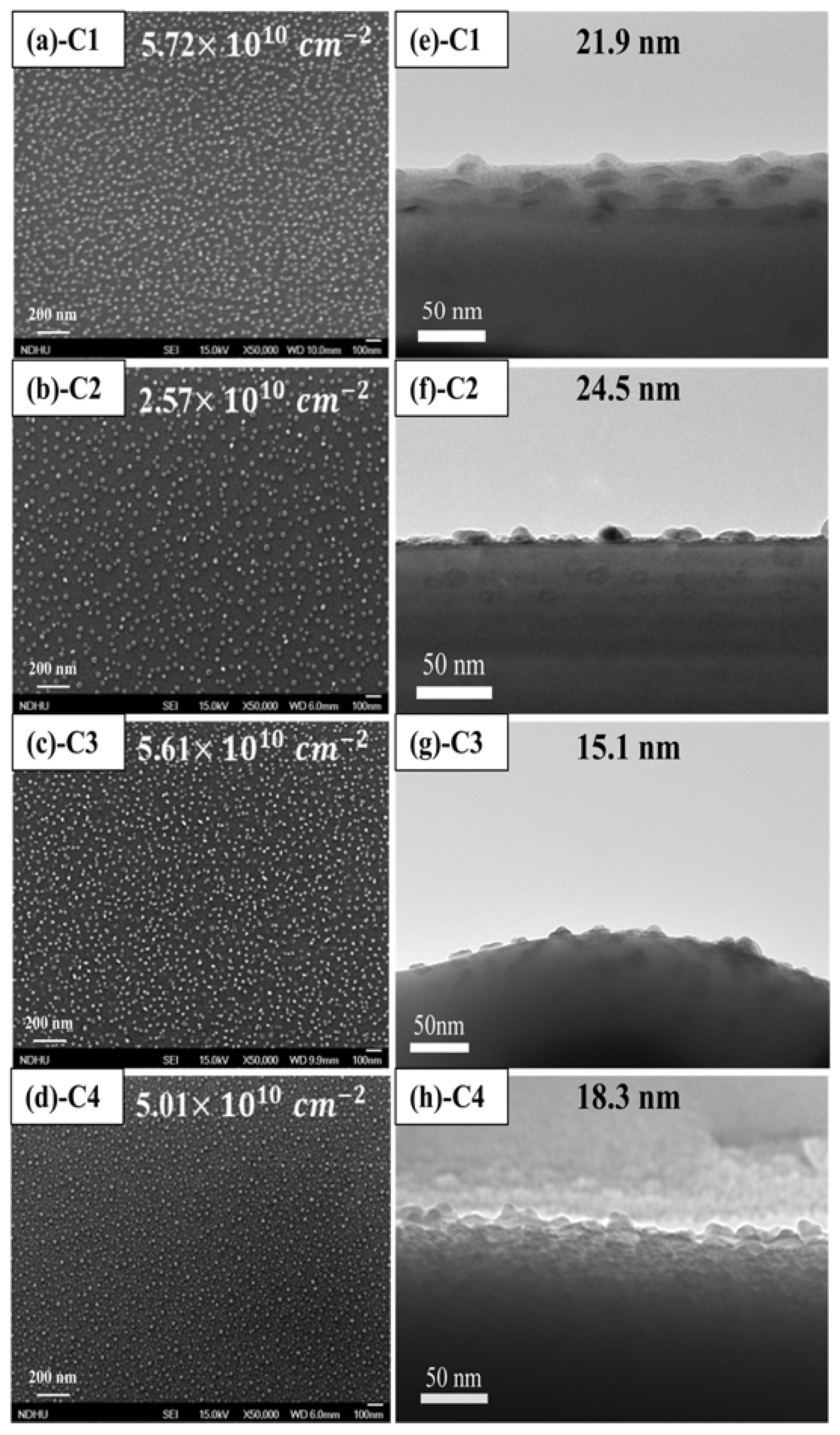
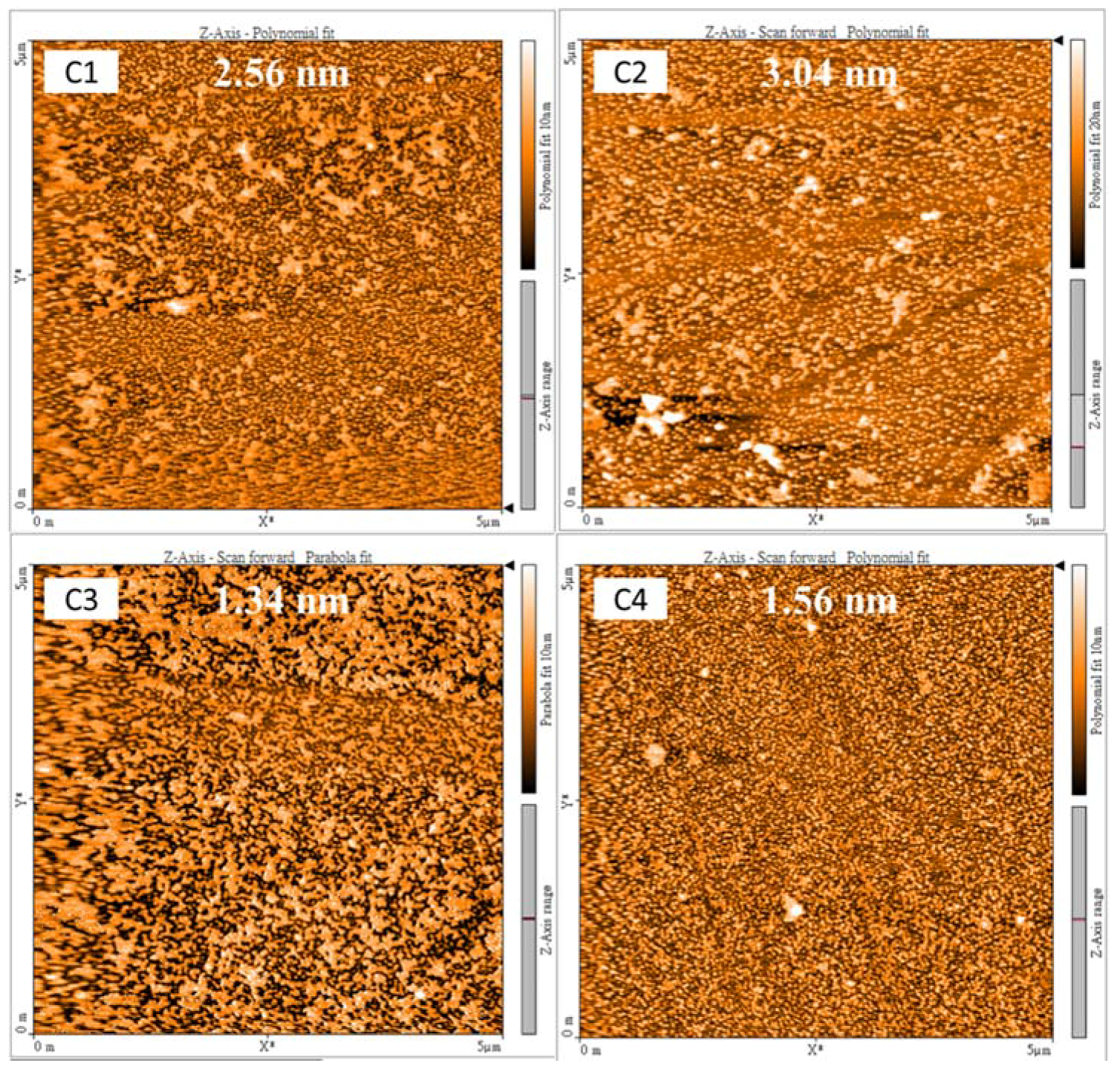
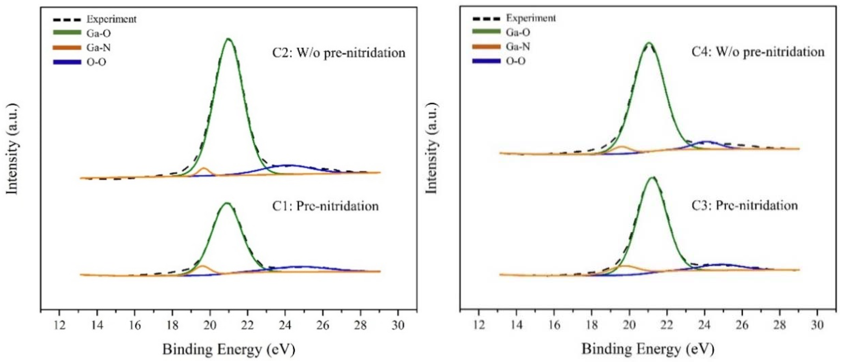
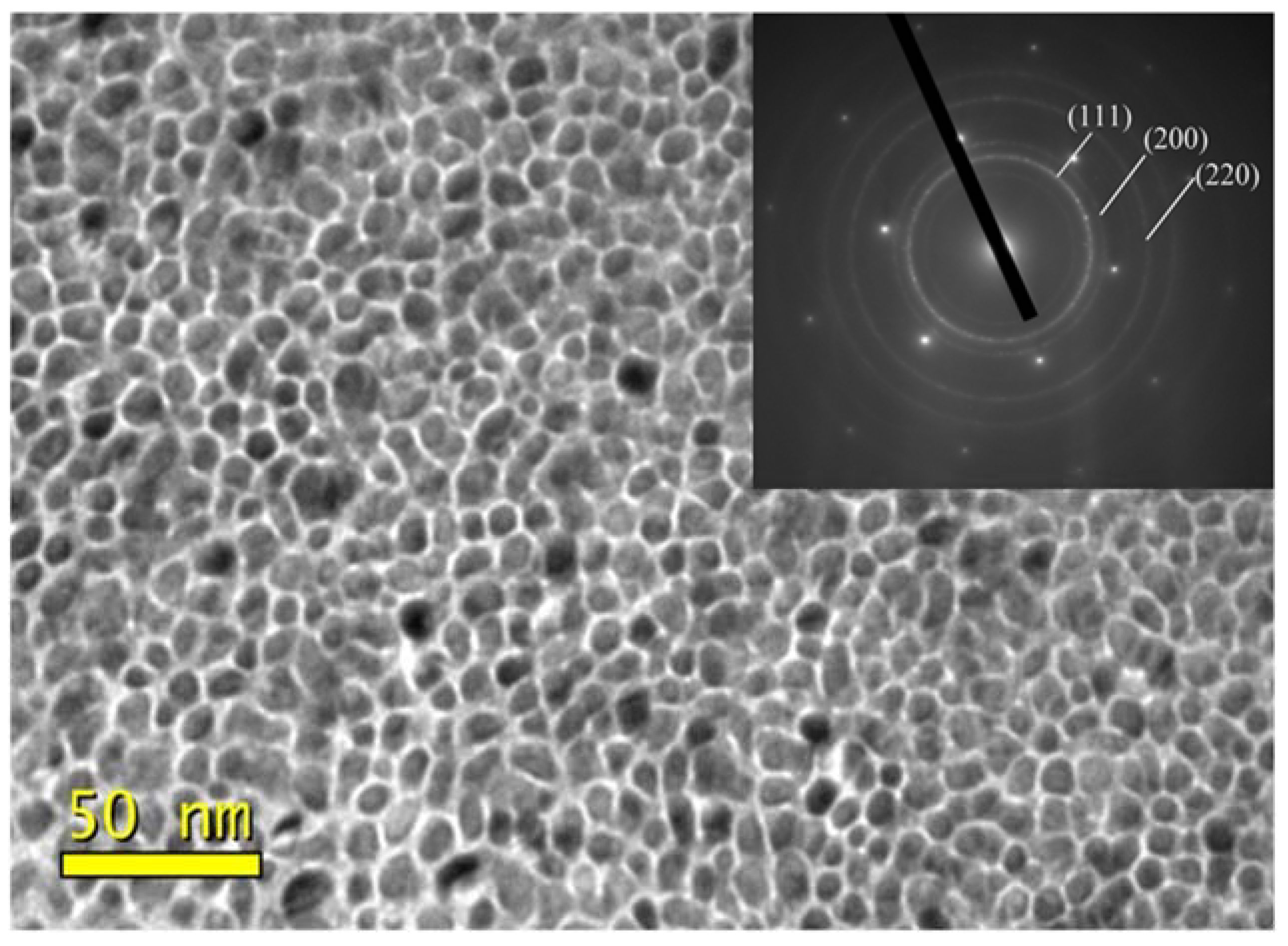
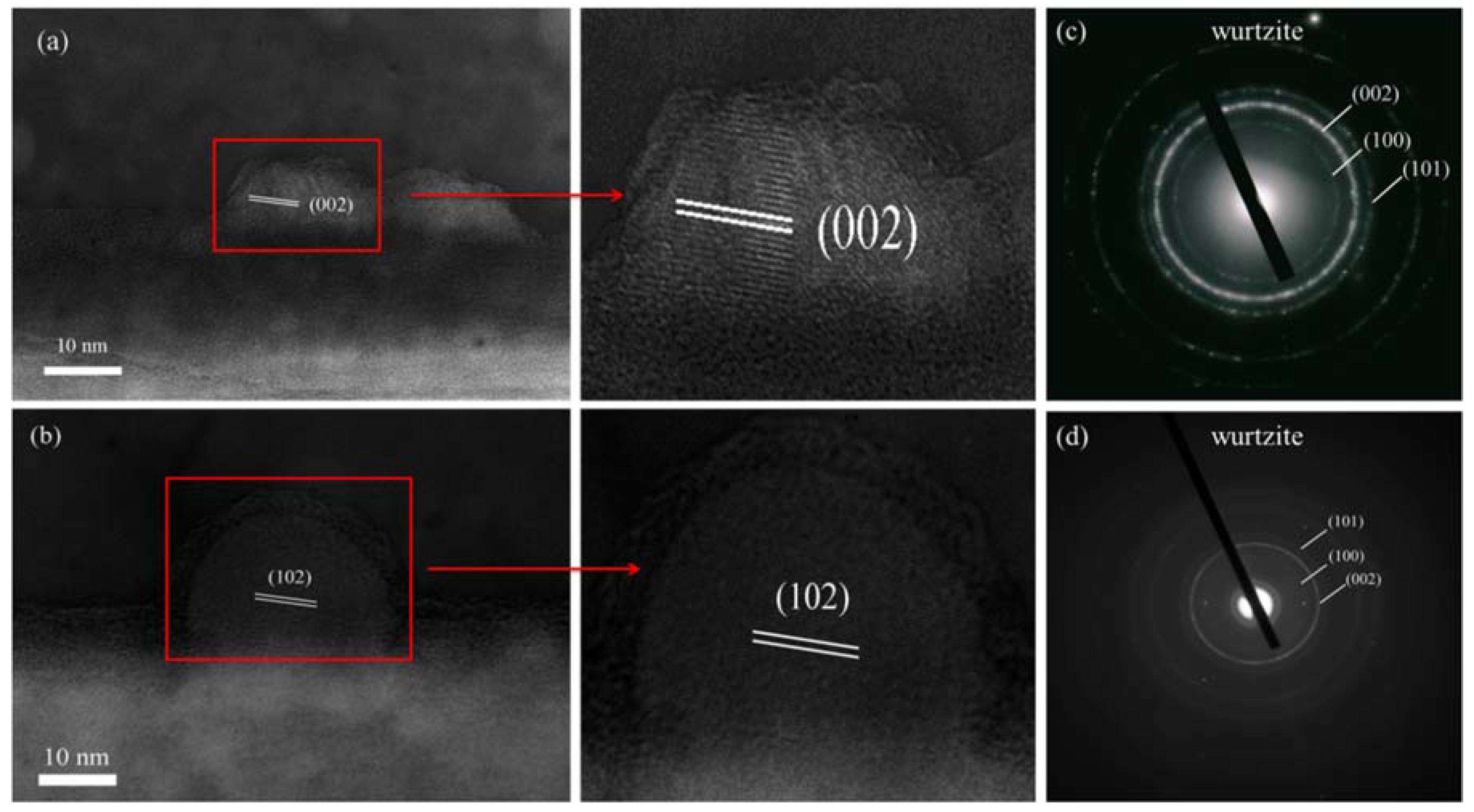
3. Results and Discussion
4. Conclusions
Author Contributions
Funding
Acknowledgments
Conflicts of Interest
References
- Wu, J. When group-III nitrides go infrared: New properties and perspectives. J. Appl. Phys. 2009, 106, 011101. [Google Scholar] [CrossRef]
- Nakamura, S.; Pearton, S.; Fasol, G. The Blue Laser Diode, 2nd ed.; Springer: Berlin, Germany, 2000. [Google Scholar]
- Su, M.; Chen, C.; Rajan, S. Prospects for the application of GaN power devices in hybrid electric vehicle drive systems. Semicond. Sci. Technol. 2013, 28, 074012. [Google Scholar] [CrossRef]
- Kako, S.; Holmes, M.; Sergent, S.; Burger, M.; As, D.J.; Arakawa, Y. Single-photon emission from cubic GaN quantum dots. Appl. Phys. Lett. 2014, 104, 011101. [Google Scholar] [CrossRef]
- Chou, H.T.; Goldhaber-Gordon, D.; Schmult, S.; Manfra, M.J.; Sergent, A.M.; Molnar, R.J. Single-electron transistors in GaN/AlGaN heterostructures. Appl. Phys. Lett. 2006, 89, 033104. [Google Scholar] [CrossRef]
- D’Amico, I.; Biolatti, E.; Rossi, F.; Derinaldis, S.; Rinaldis, R.; Cingolani, R. GaN quantum dot based quantum information/computing processing. Superlattices Microstruct. 2002, 31, 117–125. [Google Scholar] [CrossRef]
- Novikov, S.V.; Kent, A.J.; Foxon, C.T. Molecular beam epitaxy as a growth technique fpr achieving free-standing zinc-blende GaN and wurtzite AlxGa1−xN. Prog. Cryst. Growth Charact. Mater. 2017, 63, 25–39. [Google Scholar] [CrossRef]
- Susanto, I.; Kan, K.Y.; Yu, I.S. Temperature effects for GaN films grown on 4H-SiC substrate with 40 miscutting orientation by plasma-assisted molecular beam epitaxy. J. Alloys Compd. 2017, 723, 21–29. [Google Scholar] [CrossRef]
- Nakamura, S. GaN growth using GaN buffer layer. Jpn. J. Appl. Phys. 1991, 30, L1705–L1707. [Google Scholar] [CrossRef]
- Sudhir, G.S.; Fujii, H.; Wong, W.S.; Kisielowski, C.; Newman, N.; Dieker, C.; Liliental-Weber, Z.; Rubin, M.D.; Weber, E.R. Pulsed laser deposition of aluminum nitride and gallium nitride thin films. Appl. Surf. Sci. 1998, 127–129, 471–476. [Google Scholar] [CrossRef]
- Paskova, T.; Darakchieva, V.; Valcheva, E.; Paskov, P.P.; Ivanov, I.G.; Monemar, B.; Böttcher, T.; Roder, C.; Hommel, D. Hydride vapor-phase epitaxial GaN thick films for quasi-substrate applications: Strain distribution and wafer bending. J. Electron. Mater. 2004, 33, 389–394. [Google Scholar] [CrossRef]
- Brown, J.; Wu, F.; Petroff, P.M.; Speck, J.S. GaN quantum dot density control by rf-plasma molecular beam epitaxy. Appl. Phys. Lett. 2004, 84, 690–692. [Google Scholar] [CrossRef] [Green Version]
- Carlsson, N.; Seifert, W.; Petersson, A.; Castrillo, P.; Pistol, M.E.; Samuelson, L. Study of the two-dimensional–three-dimensional growth mode transition in metal-organic vapor phase epitaxy of GaInP/InP quantum-sized structures. Appl. Phys. Lett. 1994, 65, 3039. [Google Scholar] [CrossRef]
- Koguchi, N.; Tasahashi, S.; Chikyow, T. New MBE method for InSb quantum well boxes. J. Cryst. Growth 1991, 111, 688–692. [Google Scholar] [CrossRef]
- Wang, Z.M.; Holmes, K.; Mazur, Y.I.; Ramsey, K.A.; Salamo, G.J. Self-organization of quantum-dot pairs by high-temperature droplet epitaxy. Nanoscale Res. Lett. 2006, 1, 57–61. [Google Scholar] [CrossRef] [Green Version]
- Wu, C.L.; Chou, L.J.; Gwo, S. Size- and shape-controlled GaN nanocrystals grown of Si(111) substrate by reactive epitaxy. Appl. Phys. Lett. 2004, 85, 2071–2073. [Google Scholar] [CrossRef]
- Kondo, T.; Saitoh, K.; Yamamoto, Y.; Maruyama, T.; Naritsuka, S. Fabrication of GaN dot structures on Si substrates by droplet epitaxy. Phys. Stat. Sol. A 2006, 1700–1703. [Google Scholar] [CrossRef]
- Wang, Y.; Ozcan, A.S.; Sanborn, C.; Ludwig, K.F.; Bhattacharyya, A.; Chandrasekran, R.; Moustakas, T.D.; Zhou, L.; Smith, D.J. Real-time X-ray studies of gallium nitride nanodot formation by droplet heteroepitaxy. J. Appl. Phys. 2007, 102, 073522. [Google Scholar] [CrossRef]
- Yu, I.S.; Chang, C.P.; Yang, C.P.; Lin, C.T.; Ma, Y.R.; Chen, C.C. Characterization and density control of GaN nanodots on Si (111) by droplet epitaxy using plasma-assisted molecular beam epitaxy. Nanoscale Res. Lett. 2014, 9, 682. [Google Scholar] [CrossRef] [Green Version]
- Miller, D.A.B.; Chemla, D.S.; Damen, T.C.; Gossard, A.C.; Wiegmann, M.; Wood, T.H.; Burrus, C.A. Band-edge electroabsorption in quantum well structures: The quantum-confined stark effect. Phys. Rev. Lett. 1984, 53, 2173. [Google Scholar] [CrossRef]
- Naritsuka, S.; Kondo, T.; Otsubo, H.; Saitoh, K.; Yamamoto, Y.; Maruyama, T. In situ annealing of GaN dot structures grown by droplet epitaxy on (111) Si substrates. J. Cryst. Growth 2007, 300, 118–122. [Google Scholar] [CrossRef]
- Qin, H.; Luan, X.; Feng, C.; Yang, D.; Zhang, G. Mechanical, thermodynamic and electronic properties of wurtzite and zinc-blende GaN crystals. Materials 2017, 10, 1419. [Google Scholar] [CrossRef]
- Simon, J.; Pelekanos, N.T.; Adelmann, C.; Martinez-Guerrero, E.; André, R.; Daudin, B.; Dang, L.S.; Mariette, H. Direct comparison of recombination dynamics in cubic and hexagonal GaN/AlN quantum dots. Phys. Rev. B 2003, 68, 035312. [Google Scholar] [CrossRef]
- Martinez-Guerrero, E.; Chabuel, F.; Daudin, B.; Rouviere, J.L.; Mariette, H. Control of the morphology transition for the growth of cubic GaN/AlN nanostructures. Appl. Phys. Lett. 2002, 81, 5117. [Google Scholar] [CrossRef]
- Gogneau, N.; Jalabert, D.; Monroy, E.; Shibata, T.; Tanaka, M.; Daudin, B. Structure of GaN quantum dots grown under modified Stranski-Krastanow conditions on AlN. J. Appl. Phys. 2003, 94, 2254–2261. [Google Scholar] [CrossRef]
- Niu, L.; Hao, Z.; Hu, J.; Hu, Y.; Wang, L.; Luo, Y. Improving the emission efficiency of MBE-grown GaN/AlN QDs by strain control. Nanoscale Res. Lett. 2011, 6, 611. [Google Scholar] [CrossRef] [Green Version]
- Schupp, T.; Meisch, T.; Neuschl, B.; Feneberg, M.; Thonke, K.; Lischka, K.; As, D.J. Droplet epitaxy of zinc-blende GaN quantum dots. J. Cryst. Growth 2010, 312, 3235–3237. [Google Scholar] [CrossRef]
- Kawaharazuka, A.; Yoshizaki, T.; Hiratsuka, T.; Horikoshi, Y. Effect of surface Ga accumulation on the growth of GaN by molecular beam epitaxy. Phys. Status Solidi C 2010, 7, 342–346. [Google Scholar] [CrossRef]
- Copel, M.; Reuter, M.C.; Kaxiras, E.; Tromp, R.M. Surfactants in epitaxial growth. Phys. Rev. Lett. 1989, 63, 632–635. [Google Scholar] [CrossRef]
- Andrieu, S.; Frechard, P. What information can be obtained by RHEED applied on polycrystalline films? Surf. Sci. 1996, 360, 289–296. [Google Scholar] [CrossRef]
- Wang, K.; Singh, J.; Pavlidis, D. Theoretical study of GaN growth: A Monte Carlo approach. J. Appl. Phys. 1994, 76, 3502–3510. [Google Scholar] [CrossRef]
- Lymperakis, L.; Neugebauer, J. Large anisotropic adatom kinetics on nonpolar GaN surfaces: Consequences for surface morphologies and nanowire growth. Phys. Rev. B 2009, 79, 241308. [Google Scholar] [CrossRef]
- Monu, M.; Krishna, T.C.S.; Neha, A.; Mandeep, K.; Sandeep, S.; Govind, G. Pit assisted oxygen chemisorptions on GaN surface. Phys. Chem. Chem. Phys. 2015, 17, 15201–15208. [Google Scholar] [CrossRef]
- Chen, H.J.Y.; Su, Y.Z.; Yang, D.L.; Huang, T.W.; Yu, I.S. Effects of substrate pre-nitridation and post-nitridation processes on InN quantum dots with crystallinity by droplet epitaxy. Surf. Coat. Technol. 2017, 324, 491–497. [Google Scholar] [CrossRef]
- CrystOrient. Available online: http://www.crystorient.com/ (accessed on 3 April 2018).
- Romano, L.T.; Krusor, B.S.; Singh, R.; Moustakas, T.D. Structure of GaN films grown by molecular beam epitaxy on (0001) sapphire. J. Electron. Mater. 1997, 26, 285–289. [Google Scholar] [CrossRef]


| Sample | C1 | C2 | C3 | C4 |
|---|---|---|---|---|
| Pre-nitridation | Yes | No | Yes | No |
| Substrate temperature | 500 °C | 500 °C | 550 °C | 550 °C |
| Nitridation time | 5 min | 5 min | 10 min | 10 min |
© 2018 by the authors. Licensee MDPI, Basel, Switzerland. This article is an open access article distributed under the terms and conditions of the Creative Commons Attribution (CC BY) license (http://creativecommons.org/licenses/by/4.0/).
Share and Cite
Su, Y.-Z.; Yu, I.-S. Crystal Structures of GaN Nanodots by Nitrogen Plasma Treatment on Ga Metal Droplets. Metals 2018, 8, 419. https://doi.org/10.3390/met8060419
Su Y-Z, Yu I-S. Crystal Structures of GaN Nanodots by Nitrogen Plasma Treatment on Ga Metal Droplets. Metals. 2018; 8(6):419. https://doi.org/10.3390/met8060419
Chicago/Turabian StyleSu, Yang-Zhe, and Ing-Song Yu. 2018. "Crystal Structures of GaN Nanodots by Nitrogen Plasma Treatment on Ga Metal Droplets" Metals 8, no. 6: 419. https://doi.org/10.3390/met8060419
APA StyleSu, Y.-Z., & Yu, I.-S. (2018). Crystal Structures of GaN Nanodots by Nitrogen Plasma Treatment on Ga Metal Droplets. Metals, 8(6), 419. https://doi.org/10.3390/met8060419