Article

Plasma Printing of an AISI316 Micro-Meshing Punch Array for Micro-Embossing onto Copper Plates

1
Komatsu-Seiki Kosakusho, Co., Ltd., R&D section, Suwa, Nagano 392-0012, Japan
2
Surface Engineering Design Laboratory, Shibaura Institute of Technology, Ohta, Tokyo 144-0045, Japan
3
Chuo Denshi Kogyo, Co., Ltd., Ujyou, Kumamoto 869-0512, Japan
4
MICROTEX Inc., Ohta, Tokyo 144-0051, Japan
*
Author to whom correspondence should be addressed.
Metals 2019, 9(4), 396; https://doi.org/10.3390/met9040396
Submission received: 23 February 2019 / Revised: 25 March 2019 / Accepted: 27 March 2019 / Published: 30 March 2019
(This article belongs to the Special Issue Metal Micro-forming)

Abstract

:
Packaging using thermoplastic molding for hollowed GaN chips were requested for a leak-proof micro-joining between plastic molds and copper-based substrates. The design and engineering of micro-textures is a key technology for putting leak-proof packaging into practice. In the present paper, a micro-meshing punch array was prepared using plasma-nitriding-assisted printing. Two-dimensional original patterns were screen-printed onto an AISI316 die substrate and plasma nitrided at 673 K for 14.4 ks (or 4 h). The unprinted surfaces were selectively nitrogen super-saturated to have more nitrogen content than 5 mass% and a higher hardness than 1200 HV. The printed surfaces were selectively sand blasted to fabricate the micro-meshing punch array for micro-embossing. A computer numerically controlled stamping system was utilized to describe the micro-embossing behavior onto copper substrates and to investigate how the micro-textures on the array was transcribed onto the copper. Reduction of takt time as well as flexibility in the micro-grooving were discussed with reference to the picosecond laser machining and mechanical milling processes.

1. Introduction

Welding and chemical adhesion processes have been utilized as a reliable means for joining of metallic components and parts. In recent years, mechanical clinching has grown as a key manufacturing step to join dissimilar products [1] and to stack the constituent sheets into an integrated unit [2]. In particular, mechanical micro-joining is needed to make innovative packaging for power transistors and computer-processing units [3]. In those micro-joining processes, the surface to be joined must have micro-textures to increase the joining strength between two dissimilar parts, e.g., a plastic mold which must be micro-joined to a metallic substrate [4]. How to make suitable micro-textures into metallic substrates has become an urgent issue in engineering these packaging processes.
In the literature, there has been many micro-texturing methods reported, e.g., the micro-milling method [5], the micro-EDM (electrical discharging machining) method [6], and the laser micro-texturing method [7]. In the former two approaches, their micro-texturing process into a die substrate is very much dependent on the durability of thin tools and wires during the long cutting time. Although the pico-second laser machining is free from this difficulty, the total takt time for micro-texturing significantly increases in mass production. The authors [8] proposed a non-traditional method to accommodate the designed micro-textures into the molds and dies for their transcription onto the metallic and polymer sheets. In addition, an original two-dimensional micro-pattern was CAD (Computer Aided Design)-designed. Then, it was directly printed onto the DLC (Diamond Like Carbon) coatings on the die and mold surface. Plasma oxidation was utilized to remove the unprinted DLC films and to fabricate the DLC-punch array on the DLC-coated dies and molds [9,10]. Plasma nitriding was also employed to selectively nitride the unprinted surfaces and to build up the nitride-punch array by mechanical and chemical etching processes [11]. These micro-textures of the punch array were transcribed into metallic and polymer sheets via precise rolling and stamping. This selective-nitrogen embedding into stainless steel substrates came from the microstructure evolution only below the unprinted substrate surfaces [12]. Without this anisotropic microstructure evolution, this plasma-assisted printing often fails in making nitrided micro-textures into the substrate [13].
In the present paper, this plasma printing method is further advanced to fabricate a nitrided micro-meshing punch array and to make micro-embossing for transcription of this texture into the copper substrate. Screen printing was utilized to print the negative pattern onto the micro-meshing texture. These unprinted sections were selectively nitrogen-supersaturated and hardened after plasma nitriding process. The un-nitrided die parts were removed by a sandblasting process to apper the micro-meshing punch head. This micro-meshing punch was fixed onto a cassette die and was utilized to conduct micro-embossing onto a copper plate. The micro-grooves were formed onto the copper plate after micro-embossing process.

2. Experimental Procedure

An AISI316 die substrate with the size of 24 mm × 12 mm × 5 mm was utilized as a substrate material. Its surface was mirror-polished for plasma printing. The average roughness (Ra) of the AISI316 die substrate was 0.010 μm. The plasma printing procedure was stated with comments on the screen printing, the low-temperature plasma nitriding, the blasting, and the CNC (Computer Numerical Control)-micro-embossing. This present plasma printing process consists of three steps as illustrated in Figure 1. First, the negative micro-pattern of arrayed punch heads was printed as a two-dimensional mask onto the mirror-polished AISI316 substrate in Figure 1a. Figure 1b depicts the screen-printed mask pattern. Second, this printed substrate was plasma-nitrided at 673 K for 14.4 ks to make nitrogen super-saturation selectively to the unprinted substrate surfaces in Figure 1c. The printed surfaces were not nitrided and they maintained the same hardness as the matrix so that they could be mechanically removed with ease from the substrate to form the multi-punch array as shown in Figure 1d.

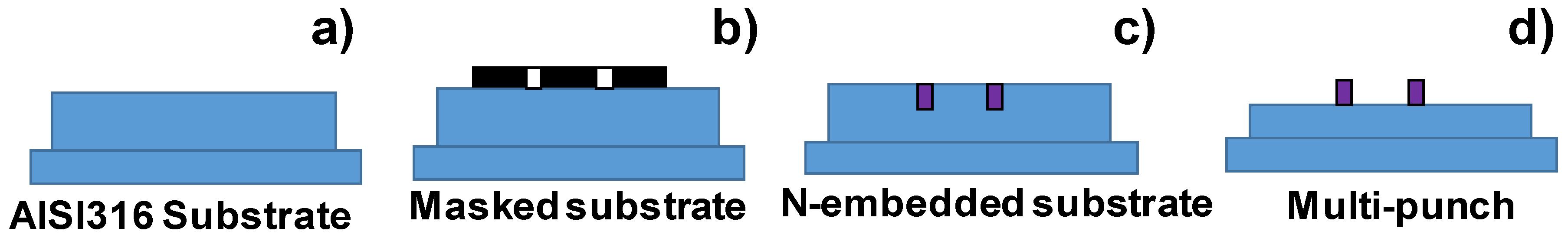
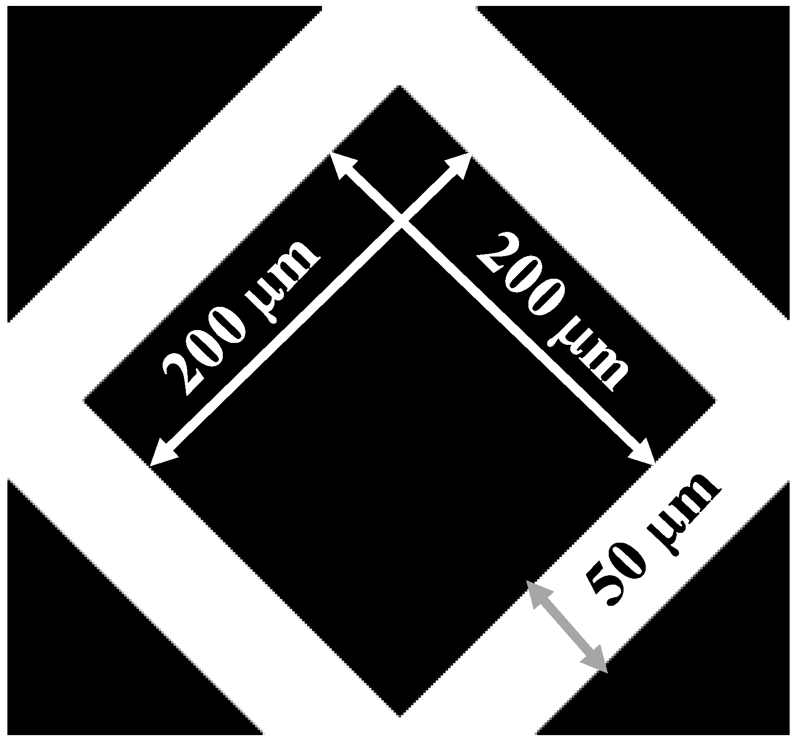
2.1. Screen Printing onto Die Substrate

The screen-printing system (NEWLONG, Co., Ltd., Shinagawa, Tokyo, Japan) was employed to print the designed micro-pattern onto the substrate’s surface after the CAD data. The mask-pattern on the screen corresponded to the arrayed multi-punch alignment. The square cell units with 200 μm × 200 μm were directly printed onto the AISI316 die surface, as shown in Figure 2. In the following experiments, a screen with a micro-meshing texture was employed to print its negative pattern onto the surface of the AISI316 die. An ink for screen-printing must be optimally selected among several candidates to have sufficient thermal resistance during the plasma nitriding at 673 K. A polymer-based ink has a risk of diminishing itself during plasma nitriding at 673 K. These inks after nitriding have to be easily removed from the processed substrate surface. In a previous study [11], a CaCO3-based ink was invented and used in trials. In the present experiment, TiO2-based ink with sufficient thermal resistance at 673 K was selected among several candidates to improve the spatial resolution in micro-patterning. In practical operations, specially formulated TiO2 ink (Teikoku Printing Inks Mfg. Co., Ltd., Arakawa, Tokyo, Japan) without the use of thinning agents was used for directly screen printing onto the die surface and dried at 673 K for 600 s in the nitrogen atmosphere.

2.2. Low-Temperature Plasma Nitriding

High-density RF (radio frequency)/DC (direct current) plasma nitriding system (YS-Electric Industry, Co., Ltd., Koufu, Yamanashi, Japan) was utilized to make selective nitrogen super-saturation to the unprinted substrate surfaces at 673 K for 14.4 ks by 70 Pa. After evacuation down to 0.1 Pa, the nitrogen gas was introduced to pre-sputter the printed die surface for 1 ks under the DC-bias of −600 V. After re-evacuation, the specimen was heated up to 673 K under the nitrogen atmosphere by 250 Pa. Then, the nitrogen hydrogen mixture gas was introduced with a flow rate of 160 mL/min for nitrogen and 30 mL/min for hydrogen, respectively. After plasma nitriding, the specimen was cooled down in the chamber under the nitrogen atmosphere. The micro-printed AISI316 substrate’s surface was fully covered by the plasma sheath with high nitrogen ion and NH-radical densities, enough to drive the nitrogen super-saturation even at lower temperatures [12]. This selective anisotropic nitrogen-embedding process results in the selective hardening and selective nitrogen concentration. The printed surface remains as a matrix hardness while the unprinted surfaces were selectively hardened up to 1400 HV for the AISI316 substrates as reported in Reference [14]. This hardness distribution by selective anisotropic nitrogen embedding drives to selectively remove the screen-printed parts from substrate.

2.3. Mechanical Blasting Process

Mechanical blasting equipment (Fuji Manufacturing Co., Ltd., Edogawa, Tokyo, Japan) was also employed to selectively remove the un-nitrided parts and masked ink from the substrate. Owing to the hardness distribution, the nitrided areas were left as a punch head while the un-nitrided areas were completely removed by this processing. Figure 3 depicts the blasting apparatus for manual operation. The blasting rate was controlled by the shooting speed of the blasting media. The punch height also varied by the duration time. In the following blasting, fine silica particles with an average diameter of 5 μm were utilized as a blasting medium. The shooting rate was constant by 2 m/s and the shooting angle by 60°. As depicted in Figure 3b, the specimen was fixed into a jig on the stage for continuous shooting operation. The duration time was selected to be 300 s in the following experiments. After Reference [11], the punch height reached 60 μm by blasting the printed parts of substrate for 300 s.

2.4. Micro-Embossing Process

The CNC stamper (Hoden Seimitsu-kako Kenkyusho, Co., Ltd., Atsugi, Kanagawa, Japan) was utilized for micro-embossing the micro-meshing punch array onto the copper specimen in Figure 4a. The multi-punch array was fixed into a cassette die in Figure 4b. This cassette die set was placed and fixed between the upper and lower bolsters in Figure 4a. The incremental loading sequence was used to control the punch stroke every 20 μm until the maximum load reached 30 kN. The total duration was 10 s for a single operation including the set-up and pick-up time of the work. An oxygen-free copper plate 20 mm × 10 mm × 1 mm was employed as a work material in the micro-embossing. The average roughness of the oxygen-free copper plate was 0.093 μm.

2.5. Evaluation Method for Micro-Embossed AISI316 Die Substrate

The AISI316 die substrate in each step of the plasma printing was evaluated by optical microscopy (STZ-168; Shimazu, Co., Ltd., Kyoto, Japan), as well as the scanning electron microscopy (SEM; JSDM-IT300LV, JEOL Ltd., Akishima, Tokyo, Japan). Energy dispersive X-ray spectroscopy (EDX; Pegasus, EDAX, Inc., Minato-ku, Tokyo, Japan) was utilized for fine element mapping. The surface roughness was measured by a three-dimensional measurement machine (Infinite-Focus; Alicona Imajing GmbH., Raaba, Graz, Austria). The hardness was measured by a micro Vickers hardness testing machine (HM-210C; Mitsutoyo Co., Ltd., Kawasaki, Kanagawa, Japan) with an applied load of 49.03 mN and for a holding time of 10 s.

3. Experimental Results

The plasma printing procedure in Figure 1 was put into practice to shape the micro-punch array with the micro-meshing heads.

3.1. Two-Dimensional Micro-Patterning onto AISI316 Die Materials

The screen was prepared to have a micro-meshing pattern with the spatial resolution of 0.2 μm as depicted in Figure 5a. The square cell units of 200 μm × 200 μm were directly printed onto the AISI316 die surface. Figure 5b shows the screen-printed micro-pattern onto the die surface. The square cell units were printed in white by using the TiO2-based ink to form the micro-meshing pattern with the line width of 50 μm and the pitch of 250 μm. Their deviation in width and pitch was within ±0.3 μm in practice.

3.2. Plasma Printing with Use of High-Density Nitrogen–Hydrogen Plasmas

Figure 6 depicts the plasma nitrided AISI316 die substrate after cleansing the masking inks. The unprinted micro-meshing lines in Figure 5b were selectively plasma nitrided to form the micro-meshing network with nitrogen super-saturated microstructure on the whole substrate surface. After References [11,12,14], the nitrided layer thickness after nitriding by the same conditions reached to 60 μm on average. Average surface hardness was measured to be 1200 HV with the standard deviation of hardness within only 30 HV.
Scanning electric microscopy as well as EDX were utilized to analyze the microstructure of the nitrided AISI316 die surface and to map nitrogen across the square cell units. As shown in Figure 7a, the micro-meshed lines were regularly aligned by the pitch of 250 μm. These lines also had higher nitrogen content than 5 mass% selectively in their widths, as analyzed in Figure 7b. Although the residuals of masking inks were left as a thin film, no height difference was seen between the masked and nitrided areas on the surface.

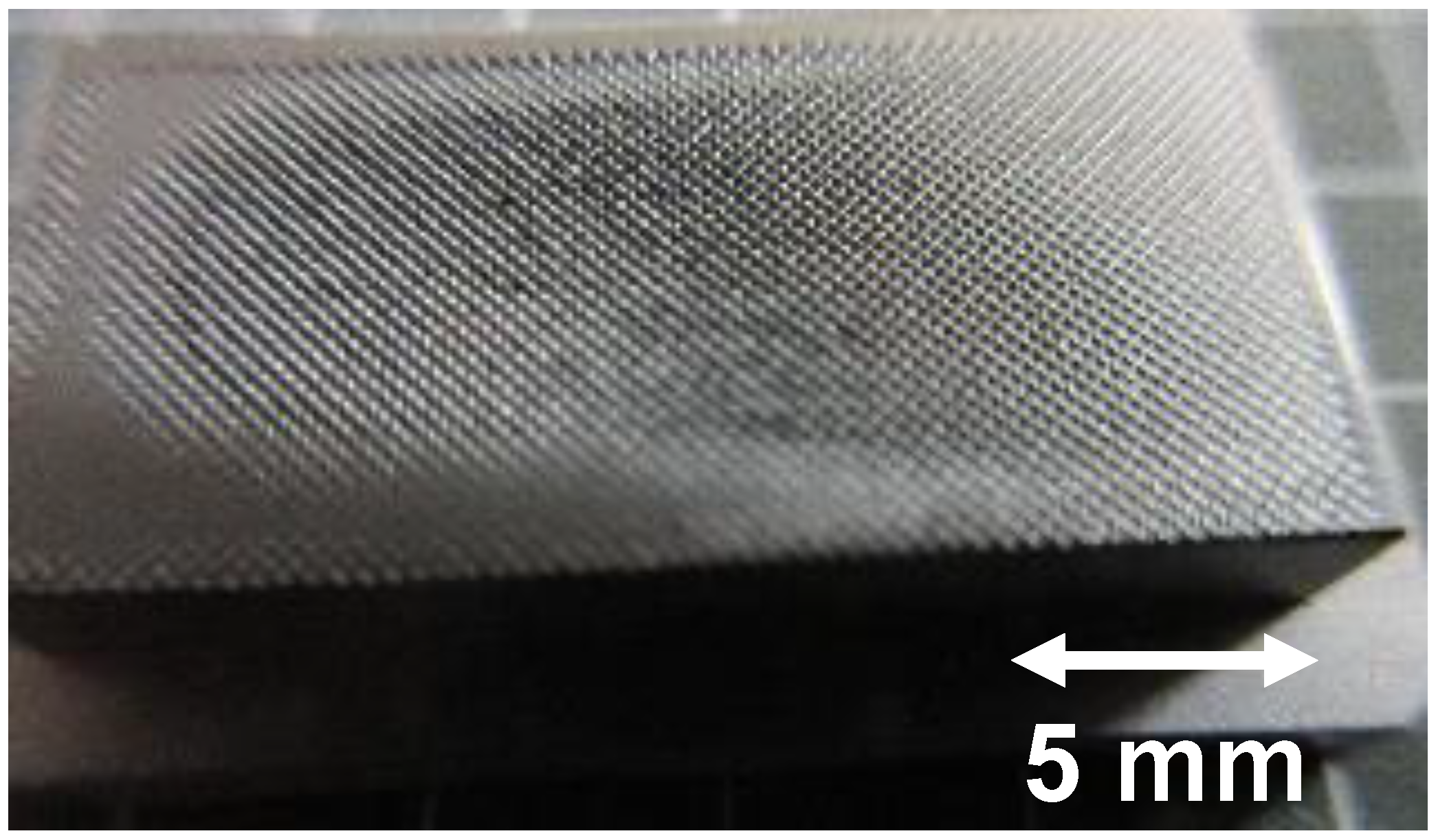
3.3. Formation of a Micro-Meshing Punch Array by Blasting Process

The blasting process was employed to remove the printed parts from the nitrided AISI316 die substrate in Figure 6 and Figure 7. Figure 8 depicts the blasted die surface. The whole surface became a multi-punch head with meshing line network. Figure 9 shows its optical microscopic image and SEM image where a square micro-cavity with a size of 180 μm × 180 μm and a depth of 75 μm was formed in regular alignment. In particular, the SEM image in a narrow range in Figure 9b proves that the un-nitrided square cells in Figure 7 were selectively dug in depth by this sand blasting to form the micro-meshed punch head array with the line width of 70 μm.

3.4. Micro-Embossing onto Copper Plates

This multi-punch die was inserted into a cassette die in Figure 4 for micro-embossing. Figure 10 shows the optical and SEM images of the micro-embossed copper plate. The multi-punch head was pushed down onto the copper plate to coin the meshed micro-grooves with the width of 70 μm. The widely scanned image in Figure 10a reveals that this coining took place uniformly on the copper surface. Each square cell with the size of 180 μm × 180 μm was backwards extruded to form a quadratic prism pillar with a maximum height of 10 μm. Metallic scratches, which were coined onto the copper plate by cold stamping, were seen on these prism head surfaces.

3.5. Transcription Processes from Micropattern on Screen to Copper Micro-Textures

A two-dimensional micropattern on the screen was transcribed into three-dimensional micro-textures on the copper plate by the present plasma printing. The micro-meshing pattern on the screen corresponds to the CAD data in Figure 11a; the white square unit cell with the edge length of 200 μm was directly printed onto the AISI316 die surface. There was little error in dimension at this step of the screen printing. Figure 11b shows the square unit cell on the nitrided AISI316 substrate at 673 K for 14.4 ks after cleansing the surface. Although thin TiO2 ink residuals overlapped at the vicinity of the mask edges and corners, the un-nitrided unit cell geometry was preserved to be a square in Figure 11b. Let us compare the unit cell geometries before and after sand blasting in Figure 11b,c. In correspondence to the original square pattern in Figure 11a, the square micro-cavities, each with an edge length of 180 μm and a depth of 75 μm, were shaped into the AISI316 die. The four edges and corners of each micro-cavity had sufficient sharpness to be working as a micro-embossing punch.
Figure 11c,d describes the micro-embossing behavior to transcribe the square unit cell. The copper was backward extruded into a square micro-cavity in the multi-punch array in Figure 9 to form the quadratic prism array with an edge length of 180 μm and a maximum height of 10 μm.
The dimensional accuracy in this plasma printing was mainly determined by the spatial resolution in screen printing. The white linear segments in Figure 11a transcribed into the micro-punch head in Figure 11c, with an average line width of 70 μm. This head width became broader than the line width of 50 μm in the original screen film because the TiO2 ink subdues and bleeds at the masking edges. This deviation of punch width was reduced by increasing the viscosity and adhesiveness of TiO2-based inks. In particular, higher viscosity ink was worked with non-subduing and non-bleeding at the square cell edges in Figure 11b. Each linear segment of the punch heads had sharp edges, even at the vicinity of cross-points as seen in Figure 11c. This edge sharpness was improved by the reduction of the edge curvature at the micro-punch shoulder via the ion beam treatment [15].
In the micro-embossing process, the copper was backward extruded to flow into each square micro-cavity of the punch by incrementally stamping the micro-meshed punch array into the copper plate as seen in Figure 10 and Figure 11d. The micro-punch heads in Figure 11c penetrate into the copper plate and formed the micro-grooves in Figure 11d. At the same time, the copper quadratic prism array was shaped on the micro-embossed copper plate by the backward extrusion. The burrs and debris were seen around the prism edges; these were also diminished by sharpening the micro-punch shoulder edges.

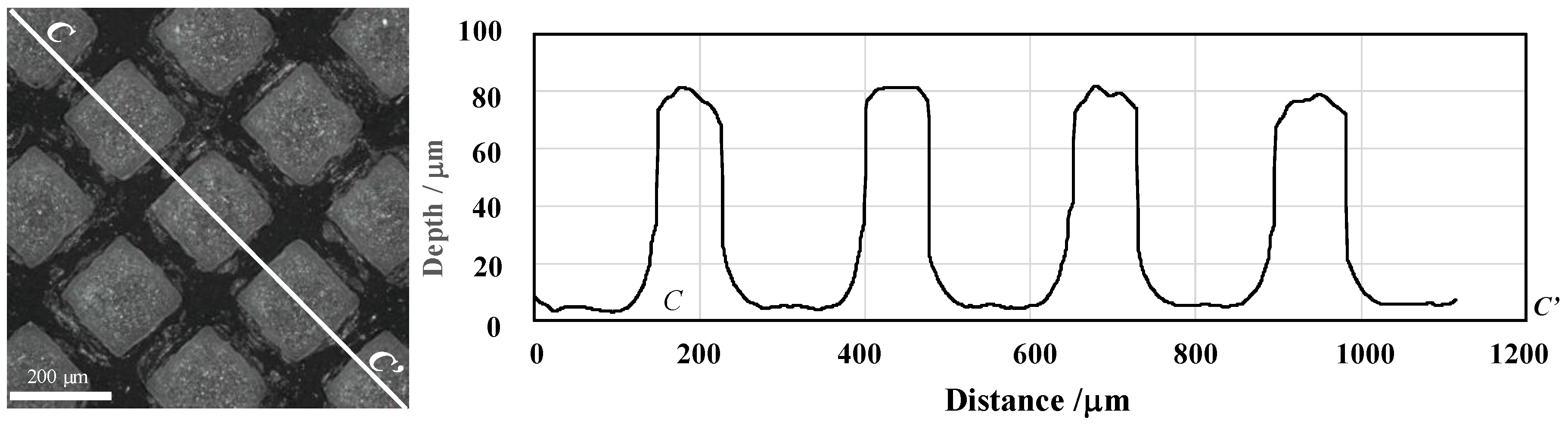
3.6. Roughness Profiles on the Punch Array Heads and the Meshed Cavities in Copper Substrate

The surface roughness on the punch array heads influenced the dimensional accuracy of the meshed copper substrate cavities. A three-dimensional profilometer was employed to measure the surface roughness profile along the line A–A’ in Figure 9b. As shown in Figure 12a, Ra of the meshed punch head surface was 1 μm except for the crossed line-heads where deep dimples were seen heterogeneously. This punch head roughness reflects on the micro-cavity quality of the copper products. Figure 12b shows the surface roughness along the line B–B’ in Figure 10b on the micro-cavities, which were cut into the copper substrate by micro-embossing. Three convex bumps were seen in correspondence to the roughness along the line A–A’ in Figure 12a. Since the dimensional deviation between two surface profiles in Figure 12 was less than 1 μm, the original surface profile on the arrayed punch heads was accurately transcribed onto the copper substrate by the present micro-embossing with use of a multi-punch array.

3.7. Evaluation of the Dimensional Accuracy of the Punch Array

A three-dimensional profilometer was also employed to measure the surface geometry of the multi-punch array. Figure 13 shows the surface geometry across four micro-punches along the line C–C’. The average height and pitch of micro-punches were 75.7 μm and 251 μm, respectively. The deviation of height was +1 μm and −2 μm among the four micro-punches. This deviation was corresponding to the surface roughness on the punch head. Each micro-punch in Figure 13 had dull shoulder edges; the borders between masked and unmasked zones might have had a lower hardness than the nitrided zone at the center of the punch head. The average head height was higher by 15 μm than the previous data of 60 μm in Reference [4]. This might be because AISI316 has a softer matrix hardness of 200 HV than the martensitic stainless steel AISI420 in Reference [4].

4. Discussion

A micro-milling process was employed to compare the processing time for the fabrication of the same micro-meshed AISI316 punch array as made by the present plasma printing. A milling tool with the diameter of 10 μm was prepared to achieve the fine corner curvatures of the micro-cavities in Figure 9 and Figure 11c. The average machining speed, cutting depth, as well as cutting distance of a single cavity layer were assumed to be 1 mm/s, 5 μm, and 2.25 mm, respectively, without fracture of the thin milling tools. Two milling paths were needed to attain the same roughness, as seen in Figure 12a. The milling time to remove a single micro-cavity 200 μm × 200 μm × 75 μm reached 120 s. Since the whole surface of a AISI316 die with the dimensions of 20 mm × 10 mm had 5000 micro-cavities (Figure 8), the total milling time became 167 h. Including the takt time to prepare the CAM (Computer Aided Machining) data for this micro-milling, the practical takt time was nearly doubled to become 320 h. The present plasma printing requires 10 min at most for screen printing, 5 h for plasma nitriding including heating and cooling, and 5 min for set-up and blasting. No CAM data were necessary since the CAD data was reflected on the screen. This comparison proves the superiority of plasma printing for fabrication of micro-punch arrays for precision mechanical milling processes.
Pico-second laser machining, as well as fiber-laser machining, have been utilized for the formation of micro-groove textures into each copper plate [3,4]. Let us evaluate the takt time for the production of the micro-textured copper plate by this plasma printing with comparison to the picosecond laser machining to make a micro-grooved copper plate. Each micro-groove has the width, depth, and pitch of 70 μm, 10 μm, and 250 μm, respectively. Then the number of micro-grooves on a copper plate with a size of 20 mm × 10 mm is counted to be 400. When using two path laser-machining, the number of paths reaches 800. When utilizing the picosecond laser with a higher repetitive frequency than 10 MHz [7], the duration time per single path is 1 s, including the on/off operation and beam positioning control. Total takt time per copper plate is 800 s. In the present approach, this takt time is reduced down to 10 s, even including the setting and stamping durations.
Microgroove textures for joining must be tailored enough to have geometric compatibility to the substrate size and chip allocation on the substrate. When using laser machining, more takt time is necessary to prepare for CAM data and to actual machining operations. The present plasma printing has intrinsic flexibility to transcribe the tailored micropattern to the multi-punch array on the die unit for micro-embossing the microgroove textures onto the copper substrate without increasing the takt time in production. Furthermore, this nitrided multi-punch array has sufficient hardness to prolong the die life in practical micro-embossing operations.

5. Conclusions

A plasma printing method with the assistance of low-temperature plasma nitriding was proposed to fabricate the micro-meshing punch array for micro-embossing the micro-groove textures onto copper plates for plastic mold packaging. A two-dimensional micro-meshing pattern with a line width of 50 μm and a pitch of 250 μm on the screen was utilized to print its negative image directly onto the AISI316 substrate’s surface. This print worked as a mask to make selective nitrogen super-saturation onto the unprinted areas. A punch array with micro-meshing textures was fabricated by blasting the printed substrate parts. This regular network of meshed punches had a meshing line width of 70 μm, height of 75 μm, and pitch of 250 μm. This array was fixed into a cassette die for micro-embossing. The takt time to fabricate this multi-punch array was significantly reduced from 320 h by precise milling process down to 6 h by the present plasma printing process. High qualification in the design of inks for screen printing is needed to improve the dimensional accuracy of punch heads.
In the micro-embossing process, copper was backwards extruded to flow into the micro-cavity array in the plasma-printed micro-punch. A quadratic prism array 180 μm × 180 μm was formed onto the copper plate. This micro-embossing process, with the use of the plasma-printed micro-punch, was useful for fabricating copper-based devices and sensors with fine alignment of prism pillars.

Author Contributions

T.S. and T.A. made the conceptual design, and planned and executed the series of experiments, with Y.S. and K.W., and wrote this paper.

Funding

This study was financially supported in part by the METI-Program for Supporting Industries in 2018.

Acknowledgments

The authors would like to express their gratitude to S. Kurozumi and H. Morita (Surface Engineering Design Laboratory, llc.), S. Hashimoto (TecDia. Co., Ltd.) and T. Yamaguchi (Sanko-Light Kogyo, Co., Ltd.), for their help in experiments.

Conflicts of Interest

The authors declare no conflict of interest.

References

  1. Balden, A. Adhesively bonded joints and repairs in metallic alloy, polymers and composite materials: Adhesives, adhesion theories and surface pretreatment. J. Mater. Sci. 2004, 39, 1–49. [Google Scholar] [CrossRef]
  2. Satoh, T.; Aizawa, T.; Shiratori, T.; Sugita, Y.; Anzai, M. Micro-joining of multi stainless steel sheets into mechanical element by low temperature diffusion process. Procedia Manuf. 2018, 15, 1475–1480. [Google Scholar] [CrossRef]
  3. Doughetty, D.; Mahalingam, M.; Viswanathan, V.; Zimmerman, M. Multi-lead organic air-cavity package for high power high frequency RFICs. In Proceedings of the 2009 IEEE MTT-S International Microwave Symposium Digest, Boston, MA, USA, 7–12 June 2009; pp. 473–476. [Google Scholar]
  4. Saito, Y.; Aizawa, T.; Wasa, K.; Nogami, Y. Leak-proof packaging for GaN chip with controlled thermal spreading and transients. In Proceedings of the 2018 IEEE BiCMOS and Compound Semiconductor Integrated Circuits and Technology Symposium, San Diego, CA, USA, 14–17 October 2018. in press. [Google Scholar]
  5. Denkena, B.; Koehler, J.; Laestner, J. Efficient machining of micro-dimples for friction reduction. In Proceedings of the 7th ICOMM, Chicago, IL, USA, 12 March 2012; pp. 85–89. [Google Scholar]
  6. Jiang, Y.; Zhao, W.S.; Kang, X.M.; Gu, L. Adaptive control for micro-hole EDM process with wavelet transform detecting method. In Proceedings of the 6th ICOMM, Tokyo, Japan, 7 September 2011; pp. 207–211. [Google Scholar]
  7. Aizawa, T.; Inohara, T. Pico- and Femtosecond Laser Micromachining for Surface Texturing; IntechOpen: London, UK, 2019. [Google Scholar]
  8. Aizawa, T.; Yamaguchi, T. Plasma nitriding assisted micro-texturing into martensitic stainless steel molds for injection molding. In Proceedings of the 9th 4M/ICOMM-2015, Milan, Italy, 26 March 2015; pp. 114–118. [Google Scholar]
  9. Aizawa, T. Micro-texturing onto amorphous carbon materials as a mold die for micro-forming. Appl. Mech. Mater. 2014, 289, 23–37. [Google Scholar] [CrossRef]
  10. Aizawa, T.; Wasa, K.; Tamagaki, H. A DLC-punch array to fabricate the micro-textured aluminum sheet for boiling heat transfer control. Micromechanics 2018, 9, 147. [Google Scholar] [CrossRef]
  11. Aizawa, T.; Saito, Y.; Yoshihara, S.-I. Micro-embossing into copper plates for mold-packaging into power semiconducting devices. In Proceedings of the 44th Autumnal Meeting of JSTP, Kumamoto, Japan, 27 October 2018; pp. 3–4. [Google Scholar]
  12. Duriagina, Z. (Ed.) Low Temperature Plasma Nitriding of Austenitic Stainless Steels; InTechOpen: London, UK, 2019; Chapter 3; pp. 31–50. [Google Scholar]
  13. Marcos, G.; Guilet, S.; Clymand, F.; Thiriet, T.; Czerwuec, T. Stainless steel patterning by combination of micro-patterning and driven strain produced by plasma assisted nitriding. Surf. Coat. Technol. 2011, 205, 5275–5279. [Google Scholar] [CrossRef]
  14. Aizawa, T.; Yoshino, T. Plastic straining for microstructural refinement in stainless steels by low temperature plasma nitriding. In Proceedings of the 12nd SEATUC Conference, YagYakarta, Indonesia, 8 March 2018; pp. 121–126. [Google Scholar]
  15. Shiratori, T.; Yoshino, T.; Suzuki, Y.; Nakano, S.; Yang, M. Effects of ion processing of cutting edge of tools on tool wear and punching characteristics in micropunching process. J. JSTP 2019, 60, 58–63. [Google Scholar] [CrossRef]
Figure 1. Plasma printing procedure in the present study. (a) The starting AISI316 substrate, (b) masked substrate by the screen printing, (c) nitrogen-embedded substrate by plasma nitriding, and (d) multi-punch formed by the blasting.
Metals 09 00396 g001
Figure 2. Geometry of a square unit cell on the screen.
Metals 09 00396 g002
Figure 3. Mechanical blasting equipment. (a) Overall image of blasting equipment and (b) the shooting stage of substrates in manual operation.
Metals 09 00396 g003
Figure 4. CNC-controlled stamper for micro-embossing onto the copper plates. (a) Overview of the CNC-stamper and (b) the cassette die set.
Metals 09 00396 g004
Figure 5. Micro-patterned AISI316 die substrate by the screen printing. (a) Micro-pattern on the screen corresponding to the CAD data and (b) the printed micropattern on the AISI316 die substrate.
Metals 09 00396 g005
Figure 6. Selectively plasma-nitrided AISI316 die substrate at 673 K for 14.4 ks.
Metals 09 00396 g006
Figure 7. Microstructure of plasma-nitrided AISI316 die surface at 673 K for 14.4 ks. (a) SEM image and (b) nitrogen mapping by EDX.
Metals 09 00396 g007
Figure 8. Multi-punch array formed on the surface of AISI316 die by sand blasting for 300 s.
Metals 09 00396 g008
Figure 9. Microscopic view of the multi-punch array. (a) Optical microscopic image in wide range of the micro-meshed punch array and (b) the SEM image in narrow.
Metals 09 00396 g009
Figure 10. Micro-embossed copper plate by incremental loading every 20 μm until the maximum load reached 30 kN. (a) Optical microscopic image in wide range and (b) the SEM image in narrow range.
Metals 09 00396 g010
Figure 11. Comparison of the geometric configurations among (a) the micropattern on the screen, (b) the SEM image of the nitrided AISI316 die, (c) the three-dimensional profile of the blasted AISI316 die, and (d) the micro-embossed copper plate.
Metals 09 00396 g011
Figure 12. Measured surface roughness profiles by three-dimensional laser profilometer. (a) Surface roughness along A–A’ in Figure 9b, and (b) surface roughness along B–B’ in Figure 10b.
Metals 09 00396 g012
Figure 13. Height distribution of the multi-punch array measured along the line C–C’. The average punch height was 76 μm.
Metals 09 00396 g013

