Abstract
Nanostructuring is considered one of the key approaches to achieve highly efficient thermoelectric alloys by reducing thermal conductivity. In this study, we investigated the effect of oxide (ZnO and SnO2) nanolayers at the grain boundaries of polycrystalline In0.2Yb0.1Co4Sb12 skutterudites on their electrical and thermal transport properties. Skutterudite powders with oxide nanolayers were prepared by atomic layer deposition method, and the number of deposition cycles was varied to control the coating thickness. The coated powders were consolidated by spark plasma sintering. With increasing number of deposition cycle, the electrical conductivity gradually decreased, while the Seebeck coefficient changed insignificantly; this indicates that the carrier mobility decreased due to the oxide nanolayers. In contrast, the lattice thermal conductivity increased with an increase in the number of deposition cycles, demonstrating the reduction in phonon scattering by grain boundaries owing to the oxide nanolayers. Thus, we could easily control the thermoelectric properties of skutterudite materials through adjusting the oxide nanolayer by atomic layer deposition method.
1. Introduction
The regulation of thermal energy is a global issue and critical for reducing global warming, which causes climate change. Various renewable and sustainable-energy-related technologies, such as energy storage and conversion materials, have been researched as alternatives to fossil fuel energy technologies. The thermoelectric (TE) technology, which allows the direct conversion of thermal energy into electrical energy without generating any pollutant, is considered the key solution to control the abundant waste heat energy [1,2,3]. The conversion efficiency of TE power generation devices is determined by the thermoelectric dimensionless figure of merit zT, which can be calculated by the equation zT = σ ∙ S2 ∙ T/κ, where S is the Seebeck coefficient, σ is the electrical conductivity, T is the absolute temperature, and κ is the total thermal conductivity of the materials. The κ includes electronic (κelec) and lattice (κlatt) contributions, with κelec governed by Wiedemann–Frantz law (κelec = L · σ · T, where L is Lorenz number) and κlatt determined by phonon scattering. Therefore, it is necessary to develop a facile method to enhance the electronic transport properties by reducing the thermal transport properties to achieve high TE performance [4,5,6].
Various TE materials have been studied in terms of their operating temperature [3]. Among them, skutterudite (SKD)-based compounds are considered one of the best candidates for medium-to-high-temperature applications owing to their good performance, stability, and mechanical properties [7,8]. Filled SKD materials with a composition of RxT4Pn12 (R = rare earth, actinide, alkali, and alkaline-earth metal; T = transition metal; Pn = pnictogen atom) composed of a cubic lattice of T4Pn12 and R elements as fillers (or rattlers), where the filler element tends to rattle, resulting in the effective scattering of lattice phonons, exhibit a low κ, representing the phonon-glass-electron-crystal model. Co4Sb12-based SKD materials show n-type conduction, and a variety of filler materials have been explored for Co4Sb12-based compounds [9,10,11,12,13,14,15]. Single elements such as In or Yb-filled n-type SKD materials have been investigated to effectively modulate the TE properties in terms of phonon scattering. He et al. reported a zT value of 1.2 for an In0.25Co4Sb12 n-type SKD material [9] and showed that the limit for In incorporation is ~0.22. A Yb-filled SKD has shown a high zT value of 1.5 for a high filling fraction of ~0.3 for Co4Sb12 [11]. Moreover, multiple filler elements are substantially used for broad-frequency phonon scattering, leading to reach high TE performance over 1.4 [13,14]. However, the Co4Sb12 mother matrix had a filling limitation for each filler element, which rendered the scattering of more phonons difficult. In addition to the control of filler composition, a different strategy such as grain boundary engineering is also required to enhance the phonon scattering of SKD materials to obtain high-performance TE materials.
Secondary phase incorporation is one of the promising technologies to enhance TE properties [15,16,17,18,19,20]. Much effort has been devoted to incorporating nanostructures such as nanoparticles or nanosheets into TE matrices. The atomic layer deposition (ALD) method, [21,22] which is typically used for thin film deposition, could be the best candidate for evaluating the effect of thin coating layer. Furthermore, the excellent conformality could be achieved even on the complex shaped substrate or powder materials [23]. The recent paper reveals that the introduction of ZnO on the grain boundary of Bi0.4Sb1.6Te3 significantly reduces the κlatt without deteriorating the electronic transport properties [18]. The effect of nanolayers at the grain boundaries introduced by ALD on the electronic and thermal transport properties of other TE materials needs to be studied.
In this study, we prepared SKD-based complex TE materials by the ALD technique and investigated the effects of nanolayer coating at the grain boundaries of SKD materials. We successfully synthesized ZnO- and SnO2-nanolayer-coated In0.2Yb0.1Co4Sb12 SKD powders by the ALD method and investigated the effect of the number of ALD cycles on the electronic and thermal transport properties.
2. Materials and Methods
An In0.2Yb0.1Co4Sb12 ingot was prepared by a typical solid-state reaction method. High-purity Co (99.998%, Alfa Aesar, Ward Hill, MA, USA), Sb (99.999%, Alfa Aesar, Ward Hill, MA, USA), In (99.999%, Alfa Aesar, Ward Hill, MA, USA), and Yb (99.9%, Alfa Aesar, Ward Hill, MA, USA) were weighed to obtain the stoichiometric composition of In0.2Yb0.1Co4Sb12 and charged into a carbon-coated quartz tube. The tube was vacuum-sealed to below 9.5 × 10⁻³ Torr, and the raw materials were melted using induction melting furnace for 20 min. The ingot was sealed again and annealed under 700 °C for one week. The ingot was pulverized using a high-energy ball mill (8000D, SPEX, Metuchen, NJ, USA) for 5 min. The resulting powder was sieved to obtain fine powder.
ZnO and SnO2 were deposited on the In0.2Yb0.1Co4Sb12 powder by ALD (iSAC Co. Ltd., iOVd100) in the temperature range of 150–350 °C using SnCl4 (99.995%, iChems Co. Ltd., Hwaseong, Korea) and (C2H5)2Zn (iChems Co. Ltd., Hwaseong, Korea), respectively, and H2O was used as an oxidant. Each deposition cycle consisted of a pulse of precursors, N2 purging, H2O pulse, and a second N2 purging process. Each purging process lasted for 20 s to allow the sufficient exhaustion of residual gases and physisorbed precursors. The precursor was supplied to the chamber with a 50 sccm flow of N2 gas. The deposition pressure was maintained as ~0.6 Torr, and 50 sccm N2 gas was continuously supplied to the chamber during the process. Each coating was applied to the In0.2Yb0.1Co4Sb12 powder with 1, 3, 5, and 100 ALD cycles.
Polycrystalline bulk samples were prepared by spark plasma sintering at 873 K for 5 min under 50 MPa in vacuum. Our bulk samples have the high density more than 96% of the theoretical density of SKD. The temperature-dependent S and σ parameters were measured from room temperature to 860 K (ZEM-3 Advanced-RIKO, Yokohama, Japan). The κ values of the samples were calculated by the equation κ = ρs · Cp ∙ λ, where ρs, Cp, and λ are the theoretical density, heat capacity, and thermal diffusivity, respectively. The λ values were measured using a laser flash installation (Laser Flash Analysis, LFA 467, Netzsch, Selb, Germany) from room temperature to 700 K. The microstructures of the ZnO and SnO2 coatings were analyzed by bright-field transmission electron microscopy (TEM, JEM-F200, JEOL, Tokyo, Japan).
3. Results and Discussion
Figure 1 shows the high-resolution TEM (HRTEM) images of the ZnO and SnO2-coated In0.2Yb0.1Co4Sb12 SKD powders after 100 cycles of ALD. As can be seen, the thickness of the ZnO layers after 100 ALD cycles is ~26 nm (Figure 1a), while that of the SnO2 layer after 100 ALD cycles is ~15 nm (Figure 1c). From the coating thicknesses, the ZnO and SnO2 ALD deposition rates were calculated as 2.60 Å/cycle and 1.50 Å/cycle, respectively. The polycrystalline ZnO and SnO2 layers were homogeneously coated on the In0.2Yb0.1Co4Sb12 SKD powder (Figure 1b,d). In addition, the selected area electron diffraction (SAED) patterns (inset images in Figure 1b,d) of the powder show concentric rings and well defined spots corresponding to the (100), (101), and (110) planes of hexagonal wurtzite ZnO and the (111) plane of orthorhombic SnO2, respectively. Thus, compared with other ALD methods reported in literature, our ALD method could synthesize homogeneous coating layers of ZnO and SnO2 on the In0.2Yb0.1Co4Sb12 SKD powder [18,19].

Figure 1.
TEM images of ZnO- and SnO2-coated In0.2Yb0.1Co4Sb12 SKD powder prepared by ALD. (a) HRTEM image and (b) bright-field TEM image of ZnO-coated In0.2Yb0.1Co4Sb12 SKD powder (inset: SAED pattern of the area enclosed in dashed red circle in Figure 1b). (c) HRTEM image and (d) bright-field TEM image of SnO2-coated In0.2Yb0.1Co4Sb12 SKD powder (inset: SAED pattern of the area enclosed in dashed red circle in (d)).
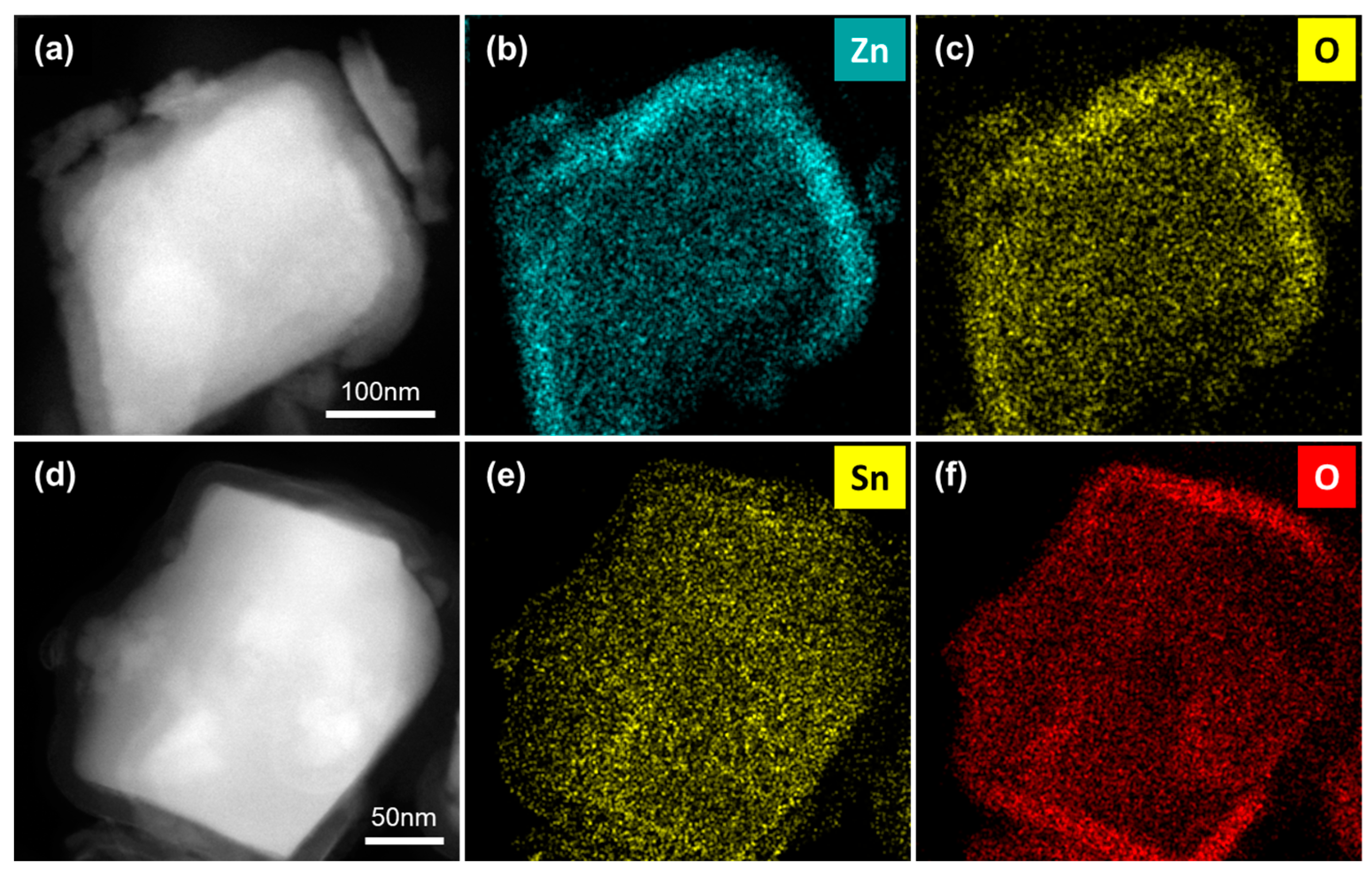
Figure 2 shows the high-angle annular dark field (HAADF) and energy dispersive X-ray spectroscopy (EDS) mapping images of the ZnO and SnO2-coated In0.2Yb0.1Co4Sb12 SKD powders after 100 ALD cycles. The bright region corresponds to the heavy elements of the In0.2Yb0.1Co4Sb12 matrix, whereas the dark region corresponds to the light elements of the ZnO or SnO2 coating layers (Figure 2a,d). The EDS mapping images of ZnO- (Figure 2b,c) and SnO2-coated In0.2Yb0.1Co4Sb12 SKD powders (Figure 2e,f) indicate the uniform coating of ZnO and SnO2 on each In0.2Yb0.1Co4Sb12 particle. This confirms that the facile ALD coating technology can produce a uniform coating of ZnO and SnO2 layers on the In0.2Yb0.1Co4Sb12 SKD powder. We expect that the homogeneous coating of oxide layer would affect the TE properties of the In0.2Yb0.1Co4Sb12 SKD material.

Figure 2.
HAADF and EDS mapping images of ZnO- and SnO2-coated In0.2Yb0.1Co4Sb12 SKD powder obtained by ALD. (a) HAADF image, (b) Zn mapping image, and (c) O mapping image of ZnO-coated In0.2Yb0.1Co4Sb12 SKD powder. (d) HAADF image, (e) Zn mapping image, and (f) O mapping image of SnO2-coated In0.2Yb0.1Co4Sb12 SKD powder.
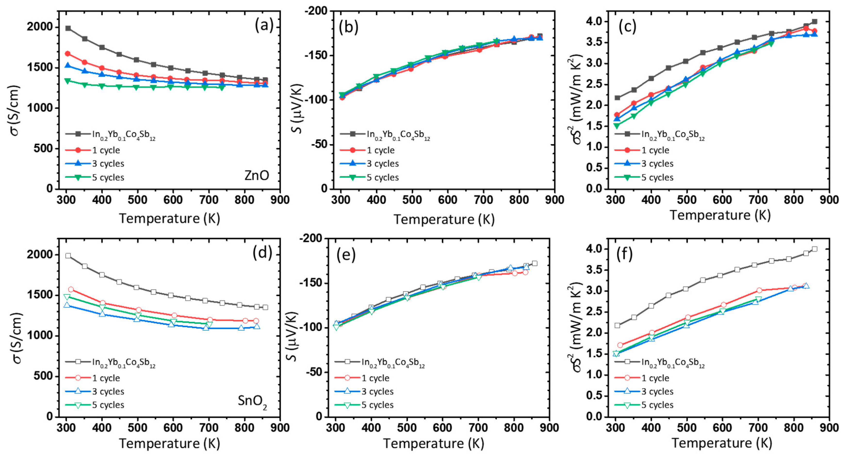
Figure 3 shows the temperature-dependent electrical transport properties (σ and S) of pristine and ZnO and SnO2-coated In0.2Yb0.1Co4Sb12. The σ of pristine In0.2Yb0.1Co4Sb12 decreased with an increase in temperature, exhibiting a metallic conduction behavior (Figure 3a). However, the conduction became less metallic with the coating of a ZnO layer, and the σ of the ZnO-coated In0.2Yb0.1Co4Sb12 after 100 ALD cycles decreased with increasing temperature, exhibiting a semiconducting behavior. With increasing number of ALD cycles, the σ decreased over the entire temperature range because of the possible electron scattering by the oxide nanolayers formed at the grain boundaries. However, interestingly, the S changed only slightly even after 100 ALD cycles (Figure 3b). This indicates that the oxide coating only affects the carrier mobility. The S at room temperature varied from 100 µV/K to 112 µV/K, while the σ at room temperature decreased from 1988 S/cm for pristine In0.2Yb0.1Co4Sb12 to 410 S/cm for ZnO-coated In0.2Yb0.1Co4Sb12 after 100 ALD cycles. Therefore, the power factor is mainly governed by the σ in this case; hence, pristine In0.2Yb0.1Co4Sb12 exhibited the highest power factor of 2.18 mW/mK2 (Figure 3c,f). For SnO2 coatings, the temperature dependences of σ and S are similar to those observed for ZnO coatings, while SnO2-coated In0.2Yb0.1Co4Sb12 exhibited a slight metallic conduction behavior even after 100 ALD cycles (Figure 3d). The S did not change significantly with increasing number of ALD coating cycles (Figure 3e). Overall, the results indicate that the coating of ZnO and SnO2 is unfavorable for the electrical transport properties of In0.2Yb0.1Co4Sb12.

Figure 3.
Electronic transport properties of ZnO- and SnO2-coated In0.2Yb0.1Co4Sb12 SKD samples prepared by ALD. (a,d) Electrical conductivity, (b,e) Seebeck coefficient, and (c,f) power factor as a function of temperature for ZnO (a–c) and SnO2 (d–f)-coated In0.2Yb0.1Co4Sb12 SKD samples.
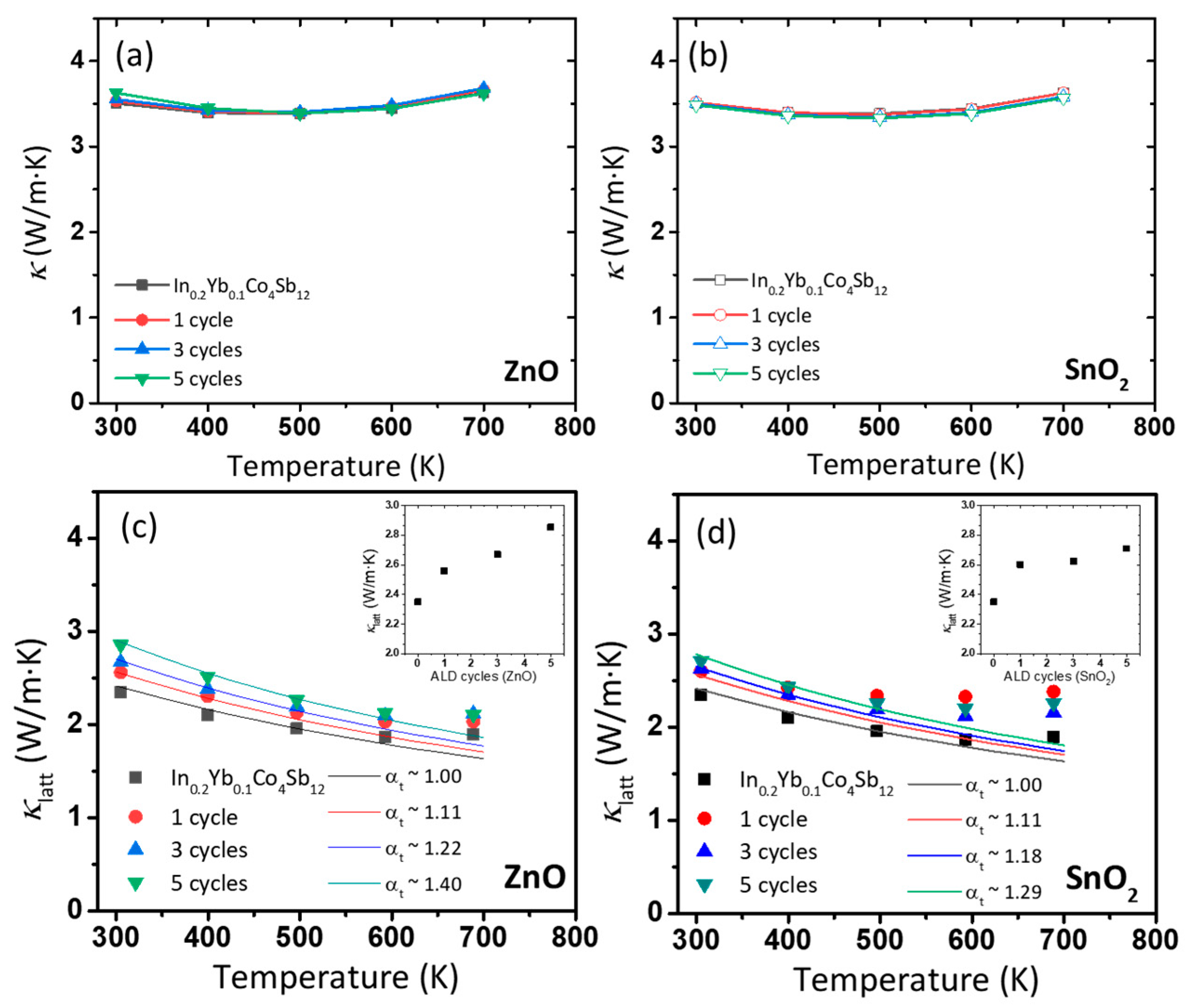
The measured κ and κlatt values are shown in Figure 4. As shown in Figure 4a,b, the samples exhibit similar κ values of 3.5 W/mK at room temperature. However, because of the decrease in σ due to the coatings, an increase in κlatt is expected despite the unchanged κ. Figure 4c,d show the calculated κlatt by deducting κelec calculated by Wiedemann–Frantz law (κelec = L · σ · T), where L is the Lorenz number, which can be estimated by Equation (1) [24].

Figure 4.
(a,b) Thermal conductivity and (c,d) lattice thermal conductivity of ZnO- and SnO2-coated In0.2Yb0.1Co4Sb12 SKD samples. The lines are calculated lattice thermal conductivity based on the Debye–Callaway model with different αt values. Insets of (c,d) show the lattice thermal conductivity at room temperature as a function of ALD cycles.
The calculated κlatt for both the coatings increased with increasing number of ALD cycles. The insets of Figure 4c,d show the κlatt at room temperature. As can be seen, the κlatt gradually increased from 2.35 to 2.85 W/mK with an increase in the number of ZnO coating cycles to five.
The κlatt is represented by Debye–Callaway model as Equation (2):
where ν, τtot, kB, ħ, θa, and z are the phonon group velocity, total phonon relaxation time, Boltzmann constant, reduced Planck’s constant, Debye temperature, and ħω/kBT, respectively. The τtot in Equation (2) is estimated from the individual relaxation time for different defect structures (τi) by Equation (3), while the inverse relaxation time for boundary phonon scattering (τB−1) is expressed as Equation (4).
Here, αt and d are the grain boundary transmission coefficient and grain size, respectively. Therefore, based on the underlying physics, changes in αt and d would lead to a modification of κlatt. In Equation (4), the αt was fitted to the experimental κlatt (symbols in Figure 4c,d) with assuming αt = 1.0 for In0.2Yb0.1Co4Sb12, while d is assumed as ~500 nm. For ZnO-coated samples, the αt becomes systematically larger to 1.11, 1.22 and 1.40 for. For SnO2 coated samples, the αt also increases systematically larger to 1.11, 1.18 and 1.29 for one, three, and five cycles. Although the fitting at high temperatures shows a discrepancy for SnO2-coated samples, the general trend of κlatt increase is maintained. The κ value generally affect both the intrinsic κ value of the certain material and the phonon scattering on the defect structures (e.g., grain boundaries). In our system, the intrinsically high κ values of ZnO and SnO2 (~50 and ~100 W/mK, respectively, at room temperature) seems to increase αt.
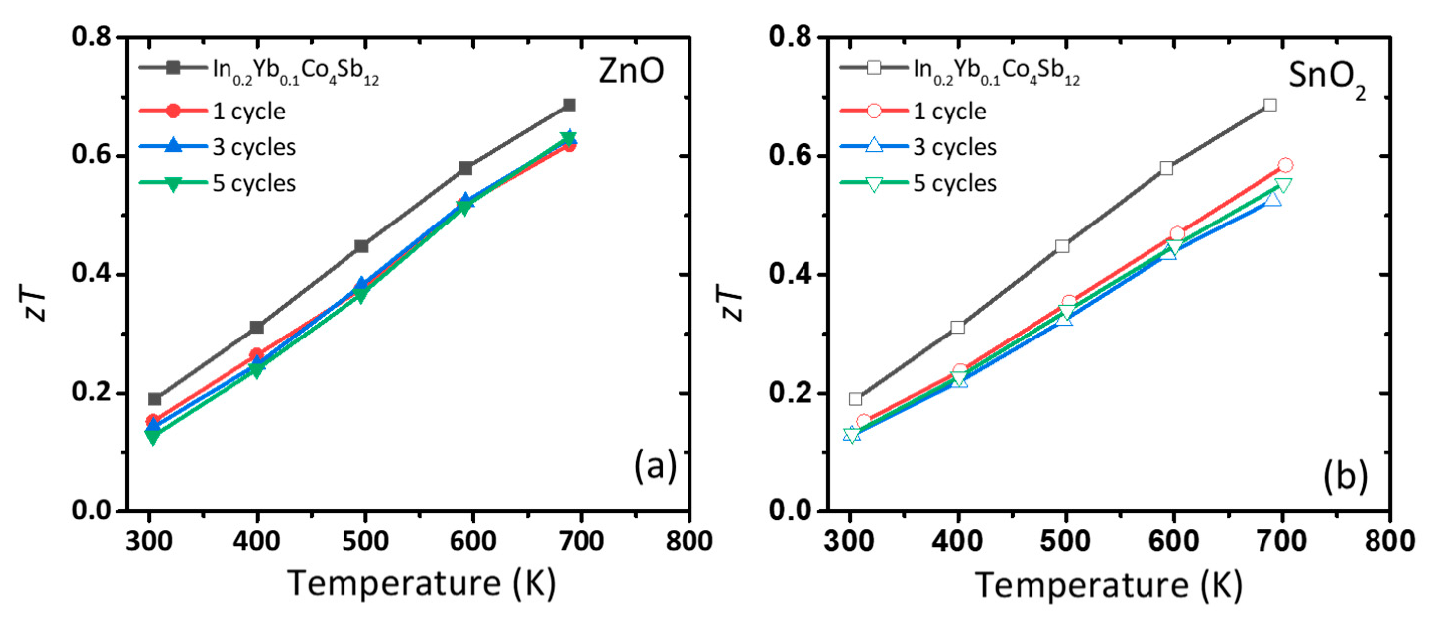
The temperature-dependent zT values of ZnO- and SnO2-coated In0.2Yb0.1Co4Sb12 are shown in Figure 5. The zT values of pristine In0.2Yb0.1Co4Sb12 and that coated with ZnO with one, three, and five cycles of ALD are 0.69, 0.62, 0.63, and 0.63, respectively, at 700 K (Figure 5a). For SnO2-coated In0.2Yb0.1Co4Sb12, the zT decreased to 0.58, 0.53, and 0.55 after one, three and five ALD cycles, respectively (Figure 5b). The change in zT value by introducing ZnO and SnO2 nanolayer does not seem positive effect in our work due to the high intrinsic κ values of selected oxide materials. However, we suggest the ALD-coated structure to control the physical properties in SKD TE materials. We believe that the fine tuning of the composition of coating layer or condition of ALD process could realize the high TE performance in SKD materials.

Figure 5.
(a,b) Thermoelectric figure of merit (zT) of ZnO and SnO2-coated In0.2Yb0.1Co4Sb12 SKD samples.
4. Conclusions
We synthesized polycrystalline In0.2Yb0.1Co4Sb12 SKD with ZnO and SnO2 oxide nanolayers at grain boundaries by an ALD process. The ALD method enables the coating of oxide nanolayers on the surfaces of SKD powders. With increasing numbers of deposition cycles, the electrical conductivity gradually decreased, while the Seebeck coefficient changed only slightly. The oxide nanolayers formed at the grain boundaries scatter the carriers, thus decreasing the mobility. In contrast, the lattice thermal conductivity increased with increasing number of deposition cycles, demonstrating the reduction in phonon scattering by grain boundaries owing to the highly thermally conductive oxide nanolayers. Thus, our work does not show the positive effect of oxide nanolayer coating on TE performance but gives a facile strategy for controlling electrical/thermal transport properties on a simple ALD process.
Author Contributions
Conceptualization, W.H.S. and J.Y.C.; methodology, W.-J.L. and S.H.K.; validation, W.H.N. and N.V.D.; formal analysis, S.-i.K. and J.A.; investigation, S.-i.K.; data curation, J.-M.O. and S.-M.K.; writing—original draft preparation, S.-i.K.; writing—review and editing, W.H.S.; supervision, W.H.S.; project administration, J.Y.C.; funding acquisition, W.H.S. All authors have read and agreed to the published version of the manuscript.
Funding
This work was supported by the Technology Innovation Program (10083640) through the Korea Evaluation Institute of Industrial Technology (KEIT) grant funded by the Ministry of Trade, Industry and Energy (MOTIE), Republic of Korea, and by Korea Institute for Advancement of Technology (KIAT) grant funded by the Korea Government (MOTIE) (P0012451, The Competency Development Program for Industry Specialist). This work was also supported by the Korea Institute of Ceramic Engineering and Technology (KPP19001).
Conflicts of Interest
The authors declare no conflict of interest.
References
- Snyder, G.J.; Toberer, E.S. Complex thermoelectric materials. Nat. Mater. 2008, 7, 105–114. [Google Scholar] [CrossRef] [PubMed]
- Disalvo, F.J. Thermoelectric Cooling and Power Generation. Science 1999, 285, 703–706. [Google Scholar] [CrossRef] [PubMed]
- Zhang, X.; Zhao, L.-D. Thermoelectric materials: Energy conversion between heat and electricity. J. Mater. 2015, 1, 92–105. [Google Scholar] [CrossRef]
- Kim, S.I.; Lee, K.H.; Mun, H.A.; Kim, H.S.; Hwang, S.W.; Roh, J.W.; Yang, D.J.; Shin, W.H.; Li, X.S.; Lee, Y.H.; et al. Dense dislocation arrays embedded in grain boundaries for high-performance bulk thermoelectrics. Science 2015, 348, 109–114. [Google Scholar] [CrossRef]
- Heremans, J.P.; Jovovic, V.; Toberer, E.S.; Saramat, A.; Kurosaki, K.; Charoenphakdee, A.; Yamanaka, S.; Snyder, G.J. Enhancement of Thermoelectric Efficiency in PbTe by Distortion of the Electronic Density of States. Science 2008, 321, 554–557. [Google Scholar] [CrossRef]
- Koh, Y.K.; Vineis, C.J.; Calawa, S.D.; Walsh, M.P.; Cahill, D.G. Lattice thermal conductivity of nanostructured thermoelectric materials based on PbTe. Appl. Phys. Lett. 2009, 94, 153101. [Google Scholar] [CrossRef]
- Rogl, P.; Rogl, P. Skutterudites, a most promising group of thermoelectric materials. Curr. Opin. Green Sustain. Chem. 2017, 4, 50–57. [Google Scholar] [CrossRef]
- Bravo, M.R.; Moure, A.; Fernández, J.F.; Martín-González, M.S. Skutterudites as thermoelectric materials: Revisited. RSC Adv. 2015, 5, 41653–41667. [Google Scholar] [CrossRef]
- He, T.; Chen, J.; Rosenfeld, H.D.; Subramanian, M.A. Thermoelectric Properties of Indium-Filled Skutterudites. Chem. Mater. 2006, 18, 759–762. [Google Scholar] [CrossRef]
- Tang, Y.; Qiu, Y.; Xi, L.; Shi, X.; Zhang, W.; Chen, L.; Tseng, S.-M.; Chen, S.-W.; Snyder, G.J. Phase diagram of In–Co–Sb system and thermoelectric properties of In-containing skutterudites. Energy Environ. Sci. 2014, 7, 812–819. [Google Scholar] [CrossRef]
- Wang, S.; Salvador, J.R.; Yang, J.; Wei, P.; Duan, B.; Yang, J. High-performance n-type YbxCo4Sb12: From partially filled skutterudites towards composite thermoelectrics. NPG Asia Mater. 2016, 8, e285. [Google Scholar] [CrossRef]
- Shi, X.; Bai, S.; Xi, L.; Yang, J.; Zhang, W.; Chen, L.; Yang, J. Realization of high thermoelectric performance in n-type partially filled skutterudites. J. Mater. Res. 2011, 26, 1745–1754. [Google Scholar] [CrossRef]
- Shi, X.; Yang, J.; Salvador, J.R.; Chi, M.; Cho, J.Y.; Wang, H.; Bai, S.; Yang, J.; Zhang, W.; Chen, L. Multiple-Filled Skutterudites: High Thermoelectric Figure of Merit through Separately Optimizing Electrical and Thermal Transports. J. Am. Chem. Soc. 2011, 133, 7837–7846. [Google Scholar] [CrossRef] [PubMed]
- Ballikaya, S.; Uzar, N.; Yildirim, S.; Salvador, J.R.; Uher, C. High thermoelectric performance of In, Yb, Ce multiple filled CoSb3 based skutterudite compounds. J. Solid State Chem. 2012, 193, 31–35. [Google Scholar] [CrossRef]
- Zhao, W.; Liu, Z.; Sun, Z.; Zhang, Q.; Wei, P.; Mu, X.; Zhou, H.; Li, C.; Ma, S.; He, D.; et al. Superparamagnetic enhancement of thermoelectric performance. Nat. Cell Biol. 2017, 549, 247–251. [Google Scholar] [CrossRef]
- Shin, W.H.; Roh, J.W.; Ryu, B.; Chang, H.J.; Kim, H.S.; Lee, S.; Seo, W.S.; Ahn, K. Enhancing Thermoelectric Performances of Bismuth Antimony Telluride via Synergistic Combination of Multiscale Structuring and Band Alignment by FeTe2 Incorporation. ACS Appl. Mater. Interfaces 2018, 10, 3689–3698. [Google Scholar] [CrossRef]
- Song, J.M.; Rahman, J.U.; Cho, J.Y.; Lee, S.; Seo, W.S.; Kim, S.; Kim, S.-I.; Lee, K.H.; Roh, D.; Shin, W.H. Chemically synthesized Cu2Te incorporated Bi-Sb-Te p-type thermoelectric materials for low temperature energy harvesting. Scr. Mater. 2019, 165, 78–83. [Google Scholar] [CrossRef]
- Kim, K.-C.; Lim, S.-S.; Lee, S.H.; Hong, J.; Cho, D.-Y.; Mohamed, A.Y.; Koo, C.M.; Baek, S.-H.; Kim, J.-S.; Kim, S.K. Precision Interface Engineering of an Atomic Layer in Bulk Bi2Te3 Alloys for High Thermoelectric Performance. ACS Nano 2019, 13, 7146–7154. [Google Scholar] [CrossRef]
- Zhang, Y.; Li, S.; Liu, F.; Zhang, C.; Hu, L.; Ao, W.; Li, Y.; Li, J.; Xie, H.; Xiao, Y.; et al. Zr vacancy interfaces: An effective strategy for collaborative optimization of ZrNiSn-based thermoelectric performance. J. Mater. Chem. A 2019, 7, 26053–26061. [Google Scholar] [CrossRef]
- Rogl, G.; Rogl, P. How nanoparticles can change the figure of merit, ZT, and mechanical properties of skutterudites. Mater. Today Phys. 2017, 3, 48–69. [Google Scholar] [CrossRef]
- Leskelä, M.; Ritala, M. Atomic Layer Deposition Chemistry: Recent Developments and Future Challenges. Angew. Chem. Int. Ed. 2003, 42, 5548–5554. [Google Scholar] [CrossRef] [PubMed]
- Lee, W.; Bera, S.; Wan, Z.; Dai, W.; Bae, J.; Hong, T.E.; Kim, K.; Ahn, J.; Kwon, S.-H. Comparative study of the electrical characteristics of ALD-ZnO thin films using H2O and H2O2 as the oxidants. J. Am. Ceram. Soc. 2019, 102, 5881–5889. [Google Scholar] [CrossRef]
- Adhikari, S.; Selvaraj, S.; Kim, D.-H. Progress in Powder Coating Technology Using Atomic Layer Deposition. Adv. Mater. Interfaces 2018, 5, 1800581. [Google Scholar] [CrossRef]
- Kim, H.-S.; Gibbs, Z.M.; Tang, Y.; Wang, H.; Snyder, G.J. Characterization of Lorenz number with Seebeck coefficient measurement. APL Mater. 2015, 3, 041506. [Google Scholar]
Publisher’s Note: MDPI stays neutral with regard to jurisdictional claims in published maps and institutional affiliations. |
© 2020 by the authors. Licensee MDPI, Basel, Switzerland. This article is an open access article distributed under the terms and conditions of the Creative Commons Attribution (CC BY) license (http://creativecommons.org/licenses/by/4.0/).


