Article

Performance and Mechanism of Photoelectrocatalytic Activity of MoSx/WO3 Heterostructures Obtained by Reactive Pulsed Laser Deposition for Water Splitting

1
National Research Nuclear University MEPhI (Moscow Engineering Physics Institute), Kashirskoe Sh. 31, 115409 Moscow, Russia
2
REC “Functional Nanomaterials”, Immanuel Kant Baltic Federal University, Aleksandra Nevskogo St. 14, 236041 Kaliningrad, Russia
*
Author to whom correspondence should be addressed.
Nanomaterials 2020, 10(5), 871; https://doi.org/10.3390/nano10050871
Submission received: 14 April 2020 / Revised: 25 April 2020 / Accepted: 28 April 2020 / Published: 30 April 2020
(This article belongs to the Special Issue Laser Synthesis and Modification of Materials at the Nanoscale)

Abstract

:
This work studies the factors that affect the efficiency of the photoelectrochemical hydrogen evolution reaction (HER) using MoSx/WO3 nano-heterostructures obtained by reactive pulsed laser deposition (RPLD) on glass substrates covered with fluorinated tin oxide (FTO). Another focus of the research is the potential of MoSx nanofilms as a precursor for MoOz(S) nanofilms, which enhance the efficiency of the photo-activated oxygen evolution reaction (OER) using the MoOz(S)/WO3/FTO heterostructures. The nanocrystalline WO3 film was created by laser ablation of a W target in dry air at a substrate temperature of 420 °C. Amorphous MoSx nanofilms (2 ≤ x ≤ 12) were obtained by laser ablation of an Mo target in H2S gas of varied pressure at room temperature of the substrate. Studies of the energy band structures showed that for all MoSx/WO3/FTO samples, photo-activated HER in an acid solution proceeded through the Z-scheme. The highest photoelectrochemical HER efficiency (a photocurrent density ~1 mA/cm2 at a potential of ~0 V under Xe lamp illumination (~100 mW/cm2)) was found for porous MoS4.5 films containing the highest concentration of catalytically active sites attributed to S ligands. During the anodic posttreatment of porous MoSx nanofilms, MoOz(S) films with a narrow energy band gap were formed. The highest OER efficiency (a photocurrent density ~5.3 mA/cm2 at 1.6 V) was detected for MoOz(S)/WO3/FTO photoanodes that were prepared by posttreatment of the MoSx~3.2 precursor. The MoOz(S) film contributed to the effective photogeneration of electron–hole pairs that was followed by the transport of photoelectrons from MoOz(S) into the WO3 film and the effective participation of holes possessing strong oxidation ability in the OER on the surface of the MoOz(S) film.

Graphical Abstract

1. Introduction

Obtaining and studying new nanomaterials for the formation of hybrid- and hetero-structures that provide effective splitting of water to produce hydrogen and oxygen is a principal task of alternative energy [1,2,3]. When creating photoelectrodes based on advanced semiconductor materials for photoelectrochemical cells, it is necessary to take into account a number of factors that affect the efficiency of water splitting. Among these factors are the optical properties of nanomaterials, their electronic structure, and the catalytic properties for activating the evolution of hydrogen and oxygen in aqueous solutions [4,5,6,7]. In the formation of hybrid/nanocomposite and hetero/multilayer structures, these factors affect the generation and transfer of non-equilibrium charge carriers (photogenerated electrons/holes) in semiconductors, the lifetime of these carriers, and the efficiency of catalytically activated processes of water splitting [8,9,10].
Tungsten oxide (WO3) is well known as a semiconducting photoactive material that has proved its effectiveness, first of all, for activating the oxygen evolution reaction (OER) [11,12,13,14]. WO3-based photoanodes, as well as photoanodes with other promising metal oxides, can be obtained by pulsed laser deposition (PLD). Variation/optimization of the PLD conditions makes it possible to obtain metal oxide photoanodes for photoelectrochemical water splitting with enhanced functional characteristics [15,16,17]. The use of this material to activate the hydrogen evolution reaction (HER) is constrained by the complexity of the formation of a specific structural and chemical state in WO3, which has high catalytic activity [18,19]. For this reason, various hybrid- and hetero-structures based on tungsten oxide are currently being developed [20,21,22,23,24,25]. In these structures, the (photo-) electrocatalytic activity of tungsten oxide is enhanced by the deposition of films (co-catalysts) that have a positive effect both on the efficiency of the electrocatalytic process of hydrogen evolution and on the processes of generation and transport of non-equilibrium carriers in a hybrid- or hetero-structure. Previously, Fominski et al. [20] showed that the efficiency of the photoelectrocatalytic HER process on WO3−y porous films can be significantly increased by the deposition of a MoSx~3/np-Mo nanofilm. MoS3/np-Mo films were produced by PLD from a MoS2 target in a buffer gas. Although the use of gas reduced the growth rate of MoS3/np-Mo films significantly, it ensured the formation of the original nanostructure, including the amorphous MoS3 phase and Mo nanoparticles. WO3−y films were created by the PLD method at room temperature of a substrate covered with fluorinated tin oxide (FTO). Thermal annealing of these films in air at 450 °C caused their crystallization, provided the porous morphology of the films did not change. The effect of annealing on the efficiency of the photoelectrocatalytic HER reaction using the (MoS3/np-Mo)/WO3−y/ FTO structures turned out to be ambiguous.
The use of nanostructured MoS3/np-Mo catalysts improves the efficiency of the HER reaction, due to both the increased sulfur concentration in the amorphous molybdenum sulfide film and the synergistic effect of Mo nanoparticles on the catalytic properties of these films. With an increase in the loading of this catalyst, however, one can expect a significant decrease in the transparency of MoS3/np-Mo films due to reflection and scattering of light by metal nanoparticles. Therefore, it is necessary to develop a different technique for producing catalytic MoSx nano-layers with a controlled concentration of sulfur atoms. This technique can be reactive PLD (RPLD), which consists of pulsed laser ablation of a Mo target in H2S (hydrogen sulfide) gas [26]. When adjusting the composition of MoSx films, their optical and electronic properties can significantly change. Therefore, for a sufficiently complete understanding of the factors affecting the efficiency of photoelectrocatalytic HER processes, the energy band structures of these molybdenum sulfides should be studied, including in a heterostructure with a sublayer of a tungsten oxide semiconductor. To create a metal oxide layer in the MoSx/WO3 heterostructure, the RPLD method from the W target in dry air of varying pressure was used. RPLD modes were selected to provide the highest film growth rate and the formation of a fairly perfect WO3 nanocrystalline structure.
The energy band distribution for MoSx/WO3 heterostructures was studied by X-ray photoelectron spectroscopy (XPS) and photospectrometry (PS). It was revealed that, regardless of the chemical composition of the MoSx films, the photo-activated HER reaction on the surface of this structure developed according to the Z-scheme. The recombination of photogenerated electrons from the conduction band (CB) of WO3 and holes from the valence band (VB) of MoSx occurred at the film’s interface, which caused a decrease in the efficiency of electron–hole pair recombination in the bulk of catalytic MoSx film. The efficiency of the HER reaction depended substantially on the composition and chemical state of MoSx films. Both parameters can be effectively controlled by changing the H2S pressure during RPLD of these films.
It is known that the MoS2 compound is modified (oxidized) in an acid solution at potentials above 1.3 V [27]. Molybdenum oxysulfide is a more stable compound, and it has shown its promise as a material for cathodes and anodes. The energy band structures of molybdenum oxides and oxysulfides largely depend on their stoichiometry [28,29,30,31]. It was of interest to use porous MoSx nanofilms as precursors for porous MoOz(S) oxysulfides with various properties as well as to study their effect on the photoelectrocatalytic characteristics of nanostructured WO3 films in the OER reaction. MoOz(S) films formed during the anodic oxidation of MoS3 films turned out to be capable of effectively activating the oxygen evolution reaction at the WO3 photoanode.
This work shows that the layered heterostructure created by the RPLD technique on an FTO-coated glass substrate and containing MoSx and WO3 nanostructured films can be used to create semiconductor photocathodes and photoanodes (after electrochemical posttreatment), which ensure efficient splitting of water under solar light. Such a structure is formed through a relatively simple method in one chamber and using one technique. Laser ablation of the W target in an oxygen-containing gas is followed by laser ablation of the Mo target in hydrogen sulfide. Qualitative photocatalytic characteristics of the heterostructure are achieved by controlling the ablation modes of the targets and by implementing optimal conditions for the deposition of a laser plume in an O- and S-containing reaction medium.

2. Materials and Methods

2.1. Reactive Pulsed Laser Deposition and Posttreatment

Reactive pulsed laser deposition of WOy and MoSx films was carried out according to standard methodology. The laser radiation was directed at an angle of 45° to the target surface. The substrate for film deposition was installed normal to the direction of expansion of the laser erosion plume and parallel to the target surface. The substrate was 4 cm distanced from the target. The Solar LQ529 (Solar LS, Minsk, Belarus) laser was used for ablation of targets made of pure (99.99%) W and Mo metals. The laser radiation had the following characteristics: a wavelength of 1064 nm, a pulse duration of 15 ns, a pulse repetition rate of 20 Hz, a pulse energy of ~100 mJ, and a laser fluence of ~15 J/cm2 on the target. After W and Mo targets and substrates were installed in the chamber to obtain films, the chamber was pumped out by a turbomolecular pump to a pressure of ~10−3 Pa. Then, dry air was let into the chamber to a predetermined pressure, and the target W was ablated. Based on the results of previous studies by Fominski et al. [20], three dry air pressures of 20, 40, and 60 Pa were chosen to produce WOy films. The temperature of the substrate was 420 °C. The deposition time of tungsten oxide films was 20 min. To prepare a layered MoSx/WOy/substrate samples for photoelectrocatalytic water splitting, 0.5-mm thick FTO coated glass plates were used as substrates. The dimensions of the RPLD-covered area of the substrate used for photoelectrochemical investigation were 0.5 × 1 cm2.
After the RPLD process to obtain tungsten oxide films was completed, the chamber was again pumped out to a pressure of 10−3 Pa. The substrate with the deposited metal-oxide film was cooled to room temperature. Then, hydrogen sulfide was injected into the chamber to a predetermined pressure, and the Mo target was ablated. To obtain MoSx films with different sulfur contents, the H2S pressure was varied from 9 to 54 Pa. To measure the composition of MoSx films and their growth rate during RPLD, preliminary experiments were performed on the deposition of these films on polished Si substrates. The estimated deposition time on Si substrates was 2 min. When these films had been analyzed, the formation time of the catalytic nanolayer in the MoSx/WOy/FTO structure was determined. The time was chosen so that the formed MoSx/WOy/FTO samples contained the same amount of Mo atoms per cm2. For this, the RPLD time for producing MoSx films for MoSx/WOy/FTO test heterostructures increased from 4.5 to 9 min with a growth in the H2S pressure from 9 to 54 Pa.
To obtain MoOz(S)/WOy/FTO photoanodes, the prepared MoSx/WOy/FTO samples were oxidized in a 0.5 M H2SO4 solution with a potential of 2 V relative to the reversible hydrogen electrode (RHE). The time of the anode posttreatment ranged from 10 to 100 s.

2.2. Structural and Chemical Characterization Techniques

To determine the composition and thickness of thin MoSx films deposited on an Si substrate, as well as WOy films deposited on an FTO substrate, Rutherford backscattering spectroscopy (RBS) of helium ions was used. Research was conducted on an accelerator at the Immanuel Kant Baltic Federal University (Kaliningrad, Russia). The ion energy in the analyzing beam was 1.5 MeV. The chosen ion scattering angle was 160 °C. The measured RBS spectra of the ions were processed using SIMNRA software (SIMNRA 7.0, Garching, Germany).
The surface morphologies of the WOy and layered MoSx/WOy films prepared on the FTO substrates were studied using scanning electron microscopy (SEM, Tescan LYRA 3, Brno, Czech Republic). FTO substrates with deposited MoSx/WOy films were split, and the fracture of the samples was studied with SEM. This procedure made it possible to examine the cross-sectional morphologies of the prepared films. The crystalline structure of WOy films deposited on the FTO substrate were investigated by grazing incidence X-ray diffraction (XRD, Cu Kα radiation, Ultima IV, Rigaku, Tokyo, Japan) and micro-Raman spectroscopy (MRS) using a 632.8-nm (He–Ne) laser. The cross-section of the laser beam was <1 μm.
To reveal the structural features of MoSx films obtained by RPLD, thin MoSx films were separated from the Si substrate in an alkaline solution. Then, they were transferred onto metal grids and studied by transmission electron microscopy and selected area electron diffraction (TEM and SAED, respectively, JEM-2100, JEOL, Tokyo, Japan). The structural state of MoSx films was also studied by MRS using a 632.8-nm (He–Ne) laser. Such studies were performed for MoSx films deposited on Si substrates. The deposition time of these films for MRS studies was increased to 10 min.
The chemical states of WOy and MoSx films were studied by XPS. XPS spectra were obtained by a Theta Probe Thermo Fisher Scientific spectrometer (Madison, WI, USA) with a monochromatic Al Kα X-ray source ( = 1486.7 eV) and an X-ray spot size of 400 μm. The spectrometer energy scale was calibrated using Au 4f7/2 core level lines located at a binding energy of 84.0 eV.

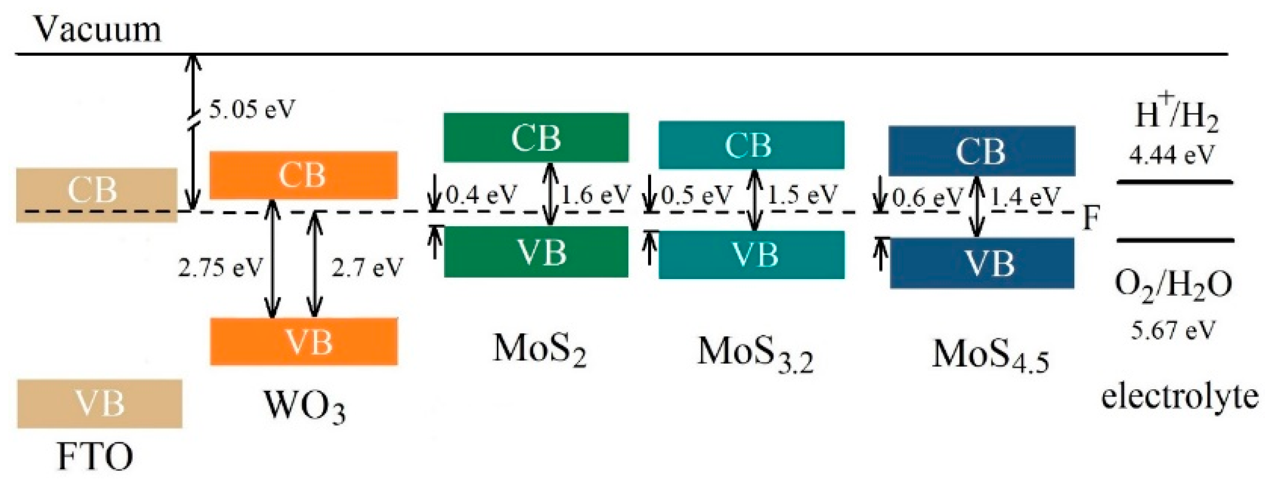
2.3. Energy Band Structure Measurements

The band gaps (Eg) for the WOy, MoSx, and MoOz(S) films were measured through the optical method by processing absorption spectra. To this end, a Tauc plot was constructed that described the dependence between (αhν)1/r and (), where α is the absorption coefficient, is the photon energy, and r is a parameter that is taken to be 2 for indirect transitions. The optical absorption and transmission spectra were measured using an Agilent Technologies Cary Series UV–Vis–NIR spectrophotometer (Santa Clara, CA, USA).
XPS measurements were used to determine the mutual arrangement of valence bands in the created semiconductor heterostructures according to a technique that is widely used at present to study the band structure in heterojunctions [32,33,34]. This method is based on determining the positions of core levels relative to the edge of the valence band for each of the semiconductors individually and as part of the heterojunction. It was assumed that the position of the core level relative to the edge of the valence band did not change when the heterojunction was formed. Then, when it was possible to determine the shift between the core levels of semiconductors in the heterojunction, the valence band offset (VBO) could be calculated. To determine VBO in MoSx/WOy and MoOz(S)/WOy heterostructures on FTO substrates, the following measurements were performed. First, the XPS spectra (binding energies, E) of the Mo 3d and W 4f core levels were measured along with the spectra of the valence bands of sufficiently thick films (more than 3 nm) on FTO substrates. Then, the spectra of the Mo 3d and W 4f core levels were measured for MoSx/WO3 and MoOz(S)/WOy heterostructures in which the thickness of the upper layer (MoSx and MoOz(S)) did not exceed 3 nm. Then, the VBO value for heterojunctions could be determined by the following formula:
VBO = (EMo3d5/2VBMMo) bulk − (EW4f7/2VBMW)bulk − (EMo3d5/2EW4f7/2)interface,
where VBMW and VBMMo are the energies of the upper edge of the valence band for WO3 and MoSx (or MoOz(S)), respectively. “Interface” stands for spectra of heterojunctions and “bulk” for spectra of thicker films on FTO substrates.
To determine the work function (φ), CutOff XPS spectra were measured. The Ekcutoff position was determined by extrapolating the tilt line to the zero baseline. The value of φ was determined by the formula φ = + EkcutoffEF(polarized), where is the energy of the quanta of the exciting X-ray radiation and EF(polarized) is the position of the Fermi level [35].

2.4. Photoelectrochemical Measurements of HER for MoSx/WOy Heterostructures

To study the photoelectrocatalytical properties of MoSx/WOy/FTO samples in HER, these samples were illuminated by radiation of Xe lamps with a power of 100 W in a 0.5 M H2SO4 aqueous solution. The light intensity was maintained at 100 mW/cm2. A three-electrode configuration was used to measure the photo-activated current in an electric circuit with modified cathodes. The polarization curves were measured using linear sweep voltammetry (LSV) with a change of the applied potential from −400 to 0 mV and a scan rate of 2 mV/s. When measuring the LSV curves and the time evolution of the photocurrent, the light source was turned on and off. For chronoamperometry measurements, the potential of the tested samples was maintained at zero level (relative to RHE).

2.5. Preparation and Characterization of MoOz(S)/WOy Photoanodes

After the MoOz(S)/WOy/FTO heterostructure had been formed by anodic posttreatment, the photoelectrocatalytic activity of these samples in the OER was studied. To do this, the polarization curves were measured with and without lighting, using linear sweep voltammetry (LSV) with an increase of the applied potential from 0 to 2 V (RHE) and a scan rate of 2 mV/s. The optical properties, chemical states, and energy bands of MoOz(S)/WOy/FTO samples were studied, which made it possible to determine the mechanism of influence of MoOz(S)films on the photoelectrocatalytic activity of WOy films in the OER process.

3. Results

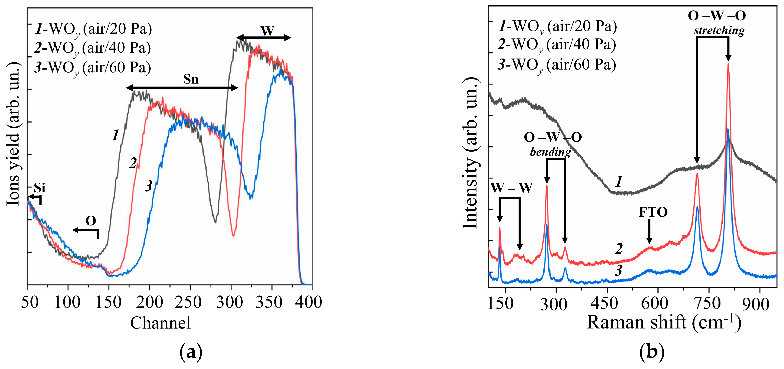
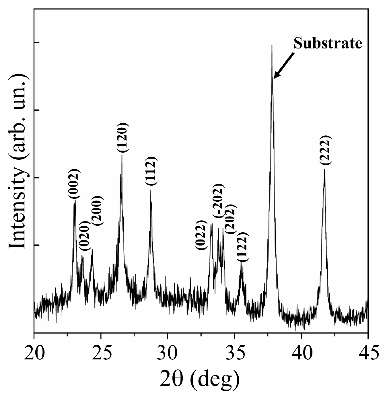
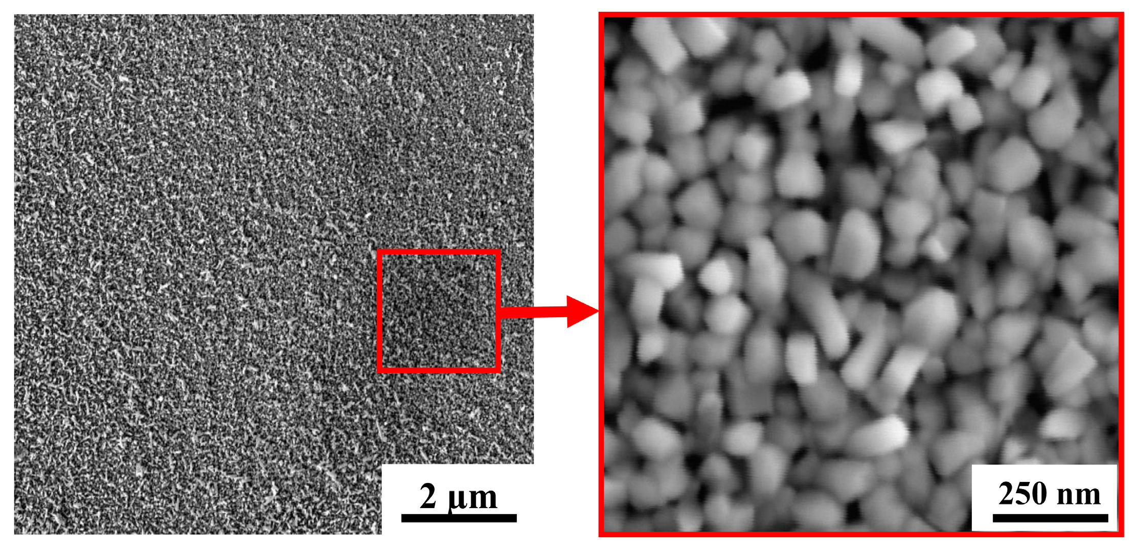
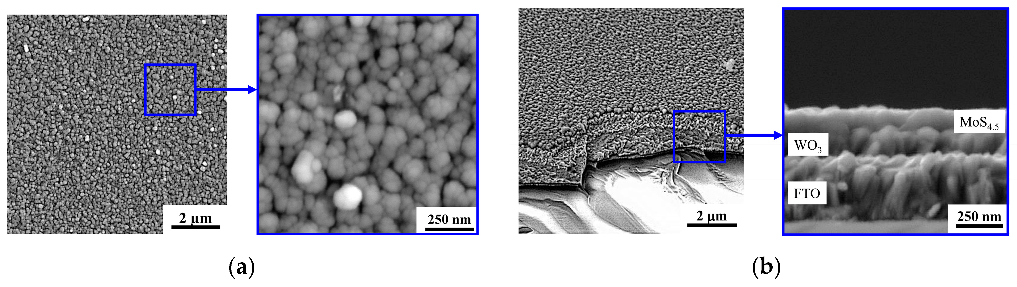
3.1. The Structure and Composition of WOy Films

Figure 1a shows RBS spectra for WOy films obtained by RPLD on FTO substrates at various pressures of dry air. The mathematical processing of these spectra using the SIMNRA software showed that an increase in dry air pressure from 20 to 60 Pa caused a decrease in the deposition rate of W atoms by about a factor of two (see Supplementary Materials, Figure S1). The estimated thickness of the WOy films decreased from ~350 to ~150 nm. Thus, the WOy film thickness (~250 nm) obtained by RPLD at dry air pressure of 40 Pa in this work was approximately equal to the thickness of the amorphous WOy film, which was obtained by RPLD previously [20]. This made it possible to reveal the effect of the structural state of the metal oxide films on the photoelectrocatalytic HER performance of MoSx/WOy heterostructures. For all the obtained WOy films, the ratio y = O/W exceeded 3. This could be due to the fact that oxygen and water molecules from the ambient air could penetrate into the pores of WOy films and remain there even when the samples were placed in a vacuum chamber for RBS studies. These results indicated a relatively low density of the formed WOy films.
MRS studies of WOy films showed (Figure 1b) that a fairly perfect crystalline structure of WOy films was formed at dry air pressures of 40 and 60 Pa. This was indicated by the peaks characteristic of the WO3 monoclinic phase at 271.8, 722.3, and 806.7 cm−1 [36,37]. In this case, no obvious differences in the MRS spectra of these films were observed. At lower dry air pressure (20 Pa), the Raman spectrum of the WOy film consisted of several broadened bands; this pointed to a strongly disordered/amorphous structure of the film. Based on the results of RBS and MRS studies, it was decided to use WOy films obtained at an air pressure of 40 Pa to form photocatalytic heterostructures. At that dry air pressure, the formation of sufficiently perfect crystalline films was observed under the condition of the highest rate of their deposition by RPLD.
Additional studies of WOy films by XPS showed (see Figure 2) that, in the case of RPLD at a dry air pressure of 40 Pa, quite effective oxidation of W atoms occurred. The XPS spectrum analysis of W 4f revealed the dominance of W6+ states with binding energies for W 4f7/2 − 4f5/2 peaks equal to 35.3 and 37.4 eV. The O 1s peak corresponding to O‒W states was located at a binding energy of 530.4 eV. The peak at 531.8 eV arose from O-containing surface contaminants. These parameters of XPS spectra for WOy films indicated the formation of a fairly perfect WO3 compound [37,38,39]. The calculation of y = O/Mo according to XPS showed that y ≈ 3. In view of the results of structural studies, WOy films obtained at a dry air pressure of 40 Pa were designated as WO3. In the analysis of XPS data for WO3 films, the possibility of the formation of W5+ (BE W 4f7/2 ~35.2 eV, BE O 1s ~531 eV) was taken into account. There was, however, no reliable confirmation that a noticeable concentration of oxygen vacancies had formed in the surface layer of these films.
XRD studies of WO3 films obtained at an air pressure of 40 Pa confirmed a fairly perfect crystalline structure of these films (Figure 3). Analysis of the XRD pattern for the WO3/FTO sample showed that sets of peaks corresponding to the WO3 phase with the P21/n (14) monoclinic lattice (PDF # 01-071-2141) were suitable for experimental peaks. In the X-ray diffraction pattern for this film, there were no peaks that would stand out in intensity among other peaks. This indicated that the film had grown in a polycrystalline mode.
Mai et al. [38] performed reactive pulsed deposition of WOy films in oxygen at 400 °C. An excimer laser was used to ablate the WO3 target. In X-ray diffraction patterns of WO3 films obtained on FTO substrates at relatively high oxygen pressures (≥13 Pa), intensity peaks at 23.6°, 24.2°, and 24.8° corresponding to the (002), (020), and (200) planes, respectively, were distinguished. The authors attributed the appearance of these peaks to the formation of a monoclinic WO3 phase, the texture of which depended substantially on the oxygen pressure. In the X-ray diffraction pattern of the WO3 film obtained using a pulsed Nd:YAG laser (Figure 3), the peaks for these planes were located at 23.1°, 23.6°, and 24.4°. The difference in lattice parameters for WO3 films obtained using solid-state and excimer lasers could be due to a combination of factors affecting film growth. Such factors include the film deposition rate (the mass of ablated material per pulse), as well as the composition and pressure of the reaction medium. The position of the peaks in the XRD pattern for the WO3 film obtained by RPLD with a solid-state laser coincided quite well with the positions of the peaks from the WO3 monoclinic phase, which was formed in WO3 films using more traditional/chemical methods for synthesizing this metal oxide (for example, [37]).
Figure 4 shows SEM images for a WO3 film deposited on an FTO substrate by RPLD at a dry air pressure of 40 Pa. The films obtained under these conditions consisted of nanocrystals in the form of up to 100-nm long nanorods. The packing density of WO3 nanocrystals was low, and they were oriented randomly relative to the film surface. Comparison of this structure with the structure of WOy<3 films, which were obtained by Fominski et al. [20] using PLD at room temperature for FTO substrates, showed that deposition on a heated FTO substrate changed the growth mechanism of WOy films and contributed to an increase in their porosity. Deposition on a heated FTO substrate disrupted the substrate-to-surface film growth and caused non-aligned growth of nanocrystals. A similar growth mechanism was found upon the deposition of WOy films on heated single-crystal SiC substrates [40]. Variation of RPLD conditions on FTO substrates did not make it possible to grow a highly porous WOy film consisting of needle nanocrystals. At all the pressures studied, films of nanorods oriented randomly relative to the surface were formed (Figure 4 and Supplementary Materials Figure S2). Previously, the formation of nanocrystals in the form of thin needles oriented perpendicular to the surface of the substrate was detected during the RPLD of WOy films on heated glassy carbon substrates [41].
Studies of the optical properties of WO3 films obtained by RPLD showed that these properties were largely comparable with the properties of WO3 films obtained by other synthesis methods [42,43]. The UV–visible absorption spectra of the RPLD WO3 film showed the absorption onset of ~450 nm, as shown in Figure 5a. The band gap was Eg ~ 2.75 eV (Figure 5b). WO3 films with a perfect crystal structure had very weak absorption in the visible region [42]. The absorption spectra of WO3 obtained by RPLD were characterized by the tailing of absorbance onset into the visible region; this indicates the presence of oxygen vacancies in the bulk of these films. The peak at 450–500 nm in the spectrum could be caused by an interference effect in multilayer films [38]. An XPS study of the valence band showed that the Fermi level was more than 2 eV away from the upper edge of the valence band (see Supplementary Materials Figure S3). The WO3 films thus had n-type conductivity due to the presence of vacancies in the crystal lattice.

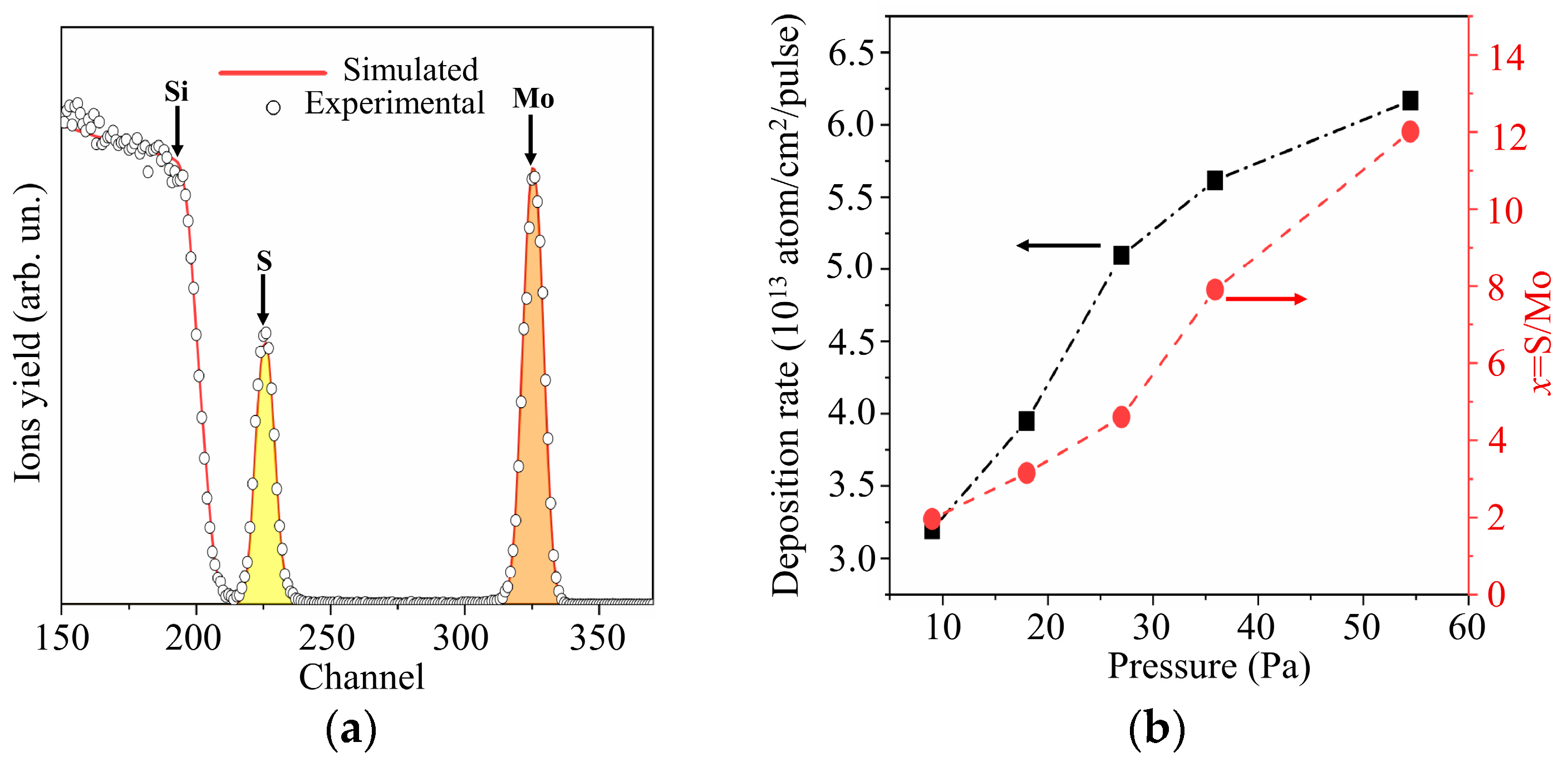
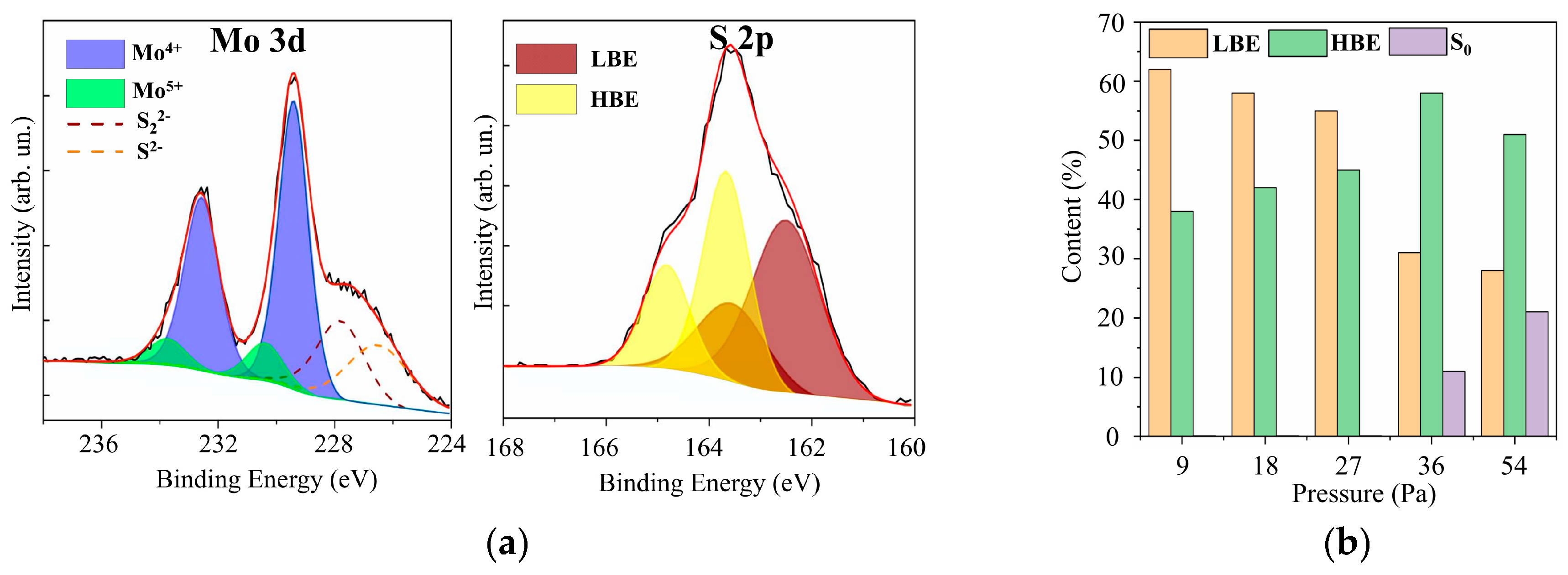
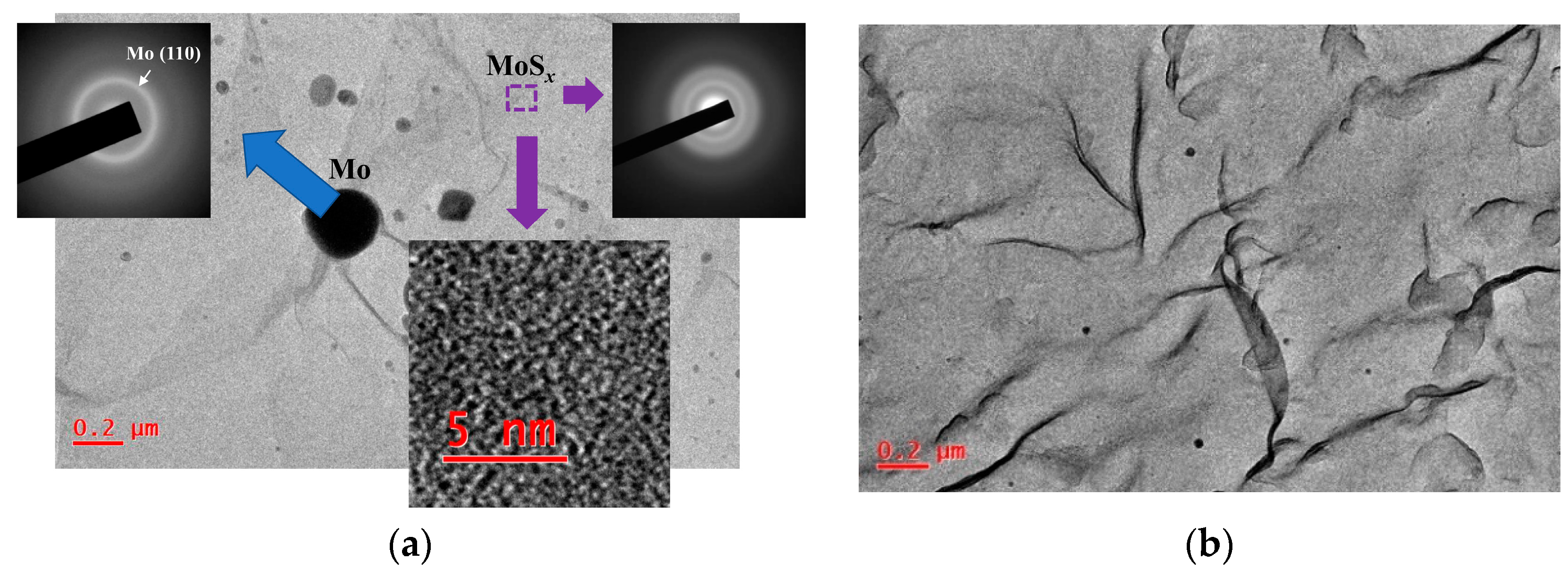
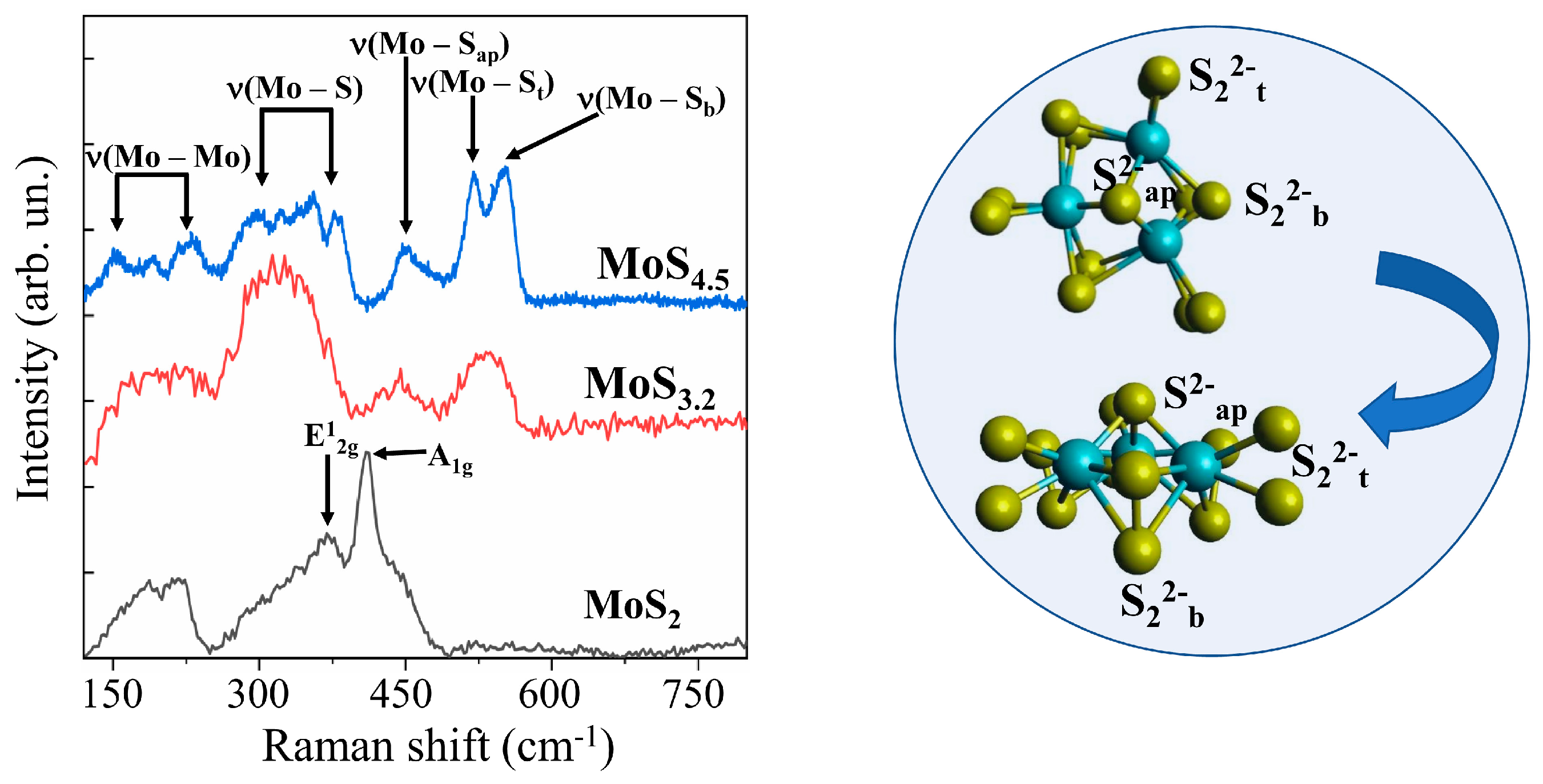
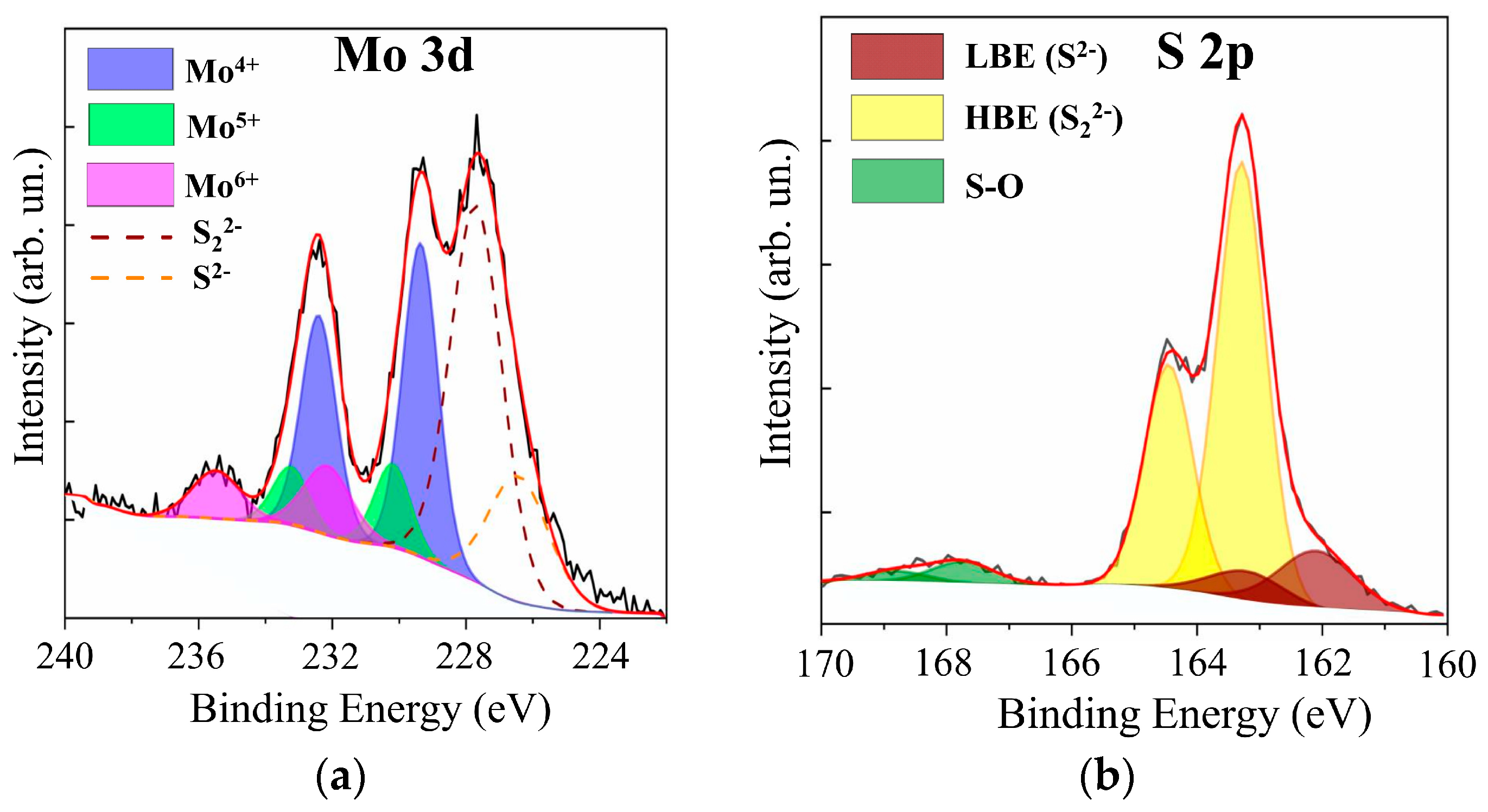
3.2. The Structure and Composition of MoSx Films

Figure 6a shows the RBS spectrum characteristic of a MoSx thin film obtained by RPLD on a polished Si substrate at an H2S pressure of 27 Pa. The experimental spectrum was in good agreement with the model spectrum, which corresponded to a MoSx film on silicon at x ~ 4.5. Figure 6b shows the results of an RBS study of MoSx films produced by RPLD at various H2S pressures. An increase in the pressure of hydrogen sulfide from 9 to 54 Pa caused an increase in the sulfur content in MoSx films. The efficiency of introducing sulfur into the films turned out to be so high that, with an increasing pressure of hydrogen sulfide, the overall deposition rate rose despite a decrease in the deposition rate of Mo atoms. The reduction in the deposition rate of Mo atoms with increasing background gas pressure is explained by the scattering of the laser plume on gas molecules [44].
Taking into account the results of RBS measurements of the sulfur content in MoSx films shown in Figure 6b, the films were designated as follows: MoS2 (pressure H2S was 9 Pa), MoS3.2 (18 Pa), MoS4.5 (27 Pa), MoS8 (36 Pa), and MoS12 (54 Pa). An XPS study of these films showed that, overall, the RBS and XPS measurements of sulfur content correlated well with each other. The x values measured by the XPS exceeded, however, by 10%–15% those measured by RBS. This could be due to the fact that, after the termination of RPLD, H2S molecules could be adsorbed on the surface of all MoSx films, and additional Mo‒S states could be formed. The efficiency of this process could not be high, since hydrogen sulfide did not show high chemical activity in the absence of laser plasma. The effect of this process on the chemical composition of the surface of MoSx films still cannot be ruled out.
In the XPS spectra of Mo 3d for films with different sulfur contents (see Figure 7 and Supplementary Materials Figure S4), two doublets Mo 3d5/2–3d3/2 corresponding to Mo4+ and Mo5+, could be distinguished. The Mo4+ state, which corresponded to the Mo 3d5/2 and 3d3/2 peaks at 229.4 eV and 232.5 eV, respectively, is formed in nanomaterials with a local atom packing characteristic of the 2H–MoS2 phase and in amorphous compounds containing 3Mo-S clusters [45,46,47]. In 3Mo-S clusters, three Mo atoms are connected in a triangle and surrounded by sulfur ligands, the features of which are manifested in S 2p spectra. The Mo5+ state is more characteristic of amorphous MoSx compounds containing Mo–S3 clusters [48,49]. In the local regions of these nanomaterials, Mo atoms are connected in a linear chain through three S atoms. For the RPLD MoS2 film, the spectrum contained a third doublet with Mo 3d5/2–3d3/2 peaks at 232.1 and 235.2 eV; this doublet corresponded to Mo6+ in compounds with oxygen. Mo–O states could form on the surface of MoSx samples after they were removed from the vacuum chamber to air [20]. With an average value of x ~ 2, on the surface of the film, there may have been local sections of sub-stoichiometric composition that interacted effectively with oxygen.
The XPS S 2p spectra analysis showed (Figure 7 and Supplementary Materials Figure S4) that these spectra contained two doublets that are usually characterized as those with low and high binding energies [45,46,47]. The S 2p3/2–2p1/2 doublet with a low binding energy (162.3 and 163.5 eV for S 2p3/2 and S 2p1/2 peaks, respectively) is characteristic of the states of S2− atoms in the crystalline MoS2 or unsaturated S2− in the amorphous MoSx [45,46,47]. The low-binding doublet may also correspond to terminal S22− in the amorphous MoSx and 3Mo-S clusters. The presence of a doublet with a high binding energy, in which S 2p3/2 and S 2p1/2 peaks had a binding energy of 163.1 and 165.0 eV, respectively, indicated the possibility of the formation of the following sulfur ligands in amorphous or clustered-type (Mo–3S and 3Mo–S) films: bridging S22−, shared S22−, and/or apical S2− [45,50,51,52].
The RPLD process at pressures of more than 36 Pa caused an increase in the sulfur concentration in MoSx films; this led, however, to the appearance of polysulfide inclusions (S0) in these films. In the XPS spectra (Supplementary Materials Figure S3) of the films obtained at a pressure of 36 Pa, a third doublet appeared, in which the S 2p3/2 peak was located near the binding energy of 164 eV. With an increase in pressure to 54 Pa, the relative intensity of this doublet increased even more. The formation of polysulfide clusters proceeds mainly under conditions of reduced chemical activity of the deposited components of MoSx films. For example, S0 polysulfide clusters were detected in MoSx films obtained by pulsed laser ablation of the MoS2 target under conditions of increased buffer gas pressure [53]. This gas could lower the energy and chemical activity of the deposited Mo and S atoms significantly; the interaction of sulfur atoms with each other became more effective than the interaction of sulfur with molybdenum. Figure 7b shows the effect of hydrogen sulfide pressure on the distribution of sulfur between the three main chemical states in MoSx films. The increase in H2S pressure caused an increase in the proportion of states characterized by a high binding energy. At pressures above 36 Pa, however, a relatively sharp decrease in the states with a low binding energy was observed, and S0 states were formed instead.
TEM/SAED studies of MoSx thin films showed that the films had an amorphous structure (Figure 8). The contrast of high-resolution TEM images consisted of randomly oriented threadlike fragments of dark and light shades. For all the MoSx films, several diffusely broadened rings were present on SAED patterns. The two most intense rings corresponded to wave vectors with modules equal to ~24 and ~35 nm−1, and they were caused by the electron diffraction in MoSx clusters. These films contained nanosized Mo particles that were ejected from the Mo target during pulsed laser ablation. The largest particle size was ~200 nm (Figure 8a). However, the concentration of such relatively large particles on the surface of the MoSx film was low. Mostly the particles smaller than 20 nm in diameter predominated (Figure 8b). The average concentration of such particles on the film surface did not exceed 10 particles per 100 μm2. These particles would not significantly affect the photoelectrochemical performance of the prepared heterostructures. It should be noted that when choosing the conditions for laser ablation of the Mo target, we tried to reduce the influence of this process. However, complete suppression of the laser-induced particle ejection from the target was difficult. The mechanisms of phase explosion and/or hydrodynamic liquid phase spraying may cause the formation of particles when intensities of the pulsed laser ablation are varied from higher to relatively low [54,55,56].
Micro-Raman spectroscopy turned out to be a more informative method for identifying the local structure features of MoSx films (Figure 9). To obtain sufficiently intense MRS spectra, thicker MoSx films were produced by RPLD. By the type of MRS spectra, all the films could be divided into three groups. In addition to the broadened bands, the MRS spectra of MoS2 films included narrow peaks at 370 and 410 cm−1. These peaks were probably due to the vibrations of A1g and E2g1 in nanoclusters with a laminar atom packing characteristic of the 2H–MoS2 phase [57]. Only a few broad peaks at 200, 320, 450, and 540 cm−1 were present in the Raman spectra of the MoS3.2 films. Such a spectrum is characteristic of amorphous nanomaterials in which there is no sufficiently perfect atomic ordering into 3Mo-S clusters [46,58]. In films with a high sulfur content (MoS4.5, MoS8, and MoS12), the local ordering of atomic packing into clusters of this type led to the appearance of narrow peaks attributed to the following vibration modes: ν(Mo–Mo) at ~200 cm−1, ν(Mo–S)coupled at ~320 cm−1, ν(Mo–Sapical) at ~450 cm−1, ν(S–S)terminal at ~520 cm−1, and ν(S–S)bridging at 540 cm−1.
Figure 10 and Supplementary Materials Figure S5 show the results of a study into the optical properties of MoSx films. These films absorbed visible light more efficiently than WO3 films did. The band gap depended weakly on the sulfur concentration and was ~1.6, 1.5, and 1.4 eV, respectively, for the MoS2, MoS3.2, and MoS4.5 films. According to the XPS studies of the valence band in quite thick MoSx films, the position of the Fermi level in the band gap depended on the sulfur concentration (see Supplementary Materials Figure S6). However, for all the films, the Fermi level was shifted closer to the valence band, which pointed to p-type conductivity mechanism in these films.
Reactive PLD of the MoSx films on the porous WO3 film led to the formation of a porous bilayer film, the characteristic SEM image of which is shown in Figure 11. Morphology of the “cauliflower” type was typical of MoSx films deposited by RPLD on glassy carbon [26]. The same morphology with a large catalytically active surface was also formed during RPLD of MoSx films on porous WO3. A separate “bush” of the MoSx film nucleated on the surface of the WO3 film, and during growth, the transverse size of the bush increased in size, reaching ~70 nm.

3.3. Electrochemical Posttreatment of MoSx Films

Figure 12 shows XPS data for the MoOz(S) film, which was obtained by anodic posttreatment of a MoS3.2 film. The anode posttreatment time at a potential of 2 V was 100 s. Comparison of this data with XPS data for the as-prepared MoS3.2 film (see Supplementary Materials Figure S4) showed that posttreatment caused a noticeable decrease in the molybdenum content in these films. The S 2s peak was equal in intensity to the Mo 3d peak. Moreover, in the XPS S 2p spectrum, the relative intensity of the doublet with a low binding energy attributed to the S2− states decreased, whereas the intensity of the doublet corresponding to the S22− states increased. XPS measurement of the film composition showed that, prior to treatment, the composition was described by the formula MoS3.3, and after the treatment, the composition was described by MoO3S8.5.
Posttreatment led to the incorporation of oxygen into the film and the formation of Mo‒O, Mo‒O‒S, and S‒O chemical bonds [30,31,59,60,61]. In the XPS Mo 3d spectrum, this was indicated by the appearance of the Mo 3d5/2–3d3/2 doublet with peak binding energies of 232.2 and 235.5 eV, respectively. This doublet pointed to the appearance of Mo6+ oxidation states. A doublet was detected in the XPS S 2p spectrum, in which S 2p3/2 and S 2p1/2 peaks had binding energy of 167.8 and 168.5 eV, respectively. The posttreatment of MoS3.2 films caused an increase in the contribution of the doublet that corresponded to the Mo5+ oxidation state to the XPS Mo 3d spectrum. The ratio of Mo5+/Mo4+ increased from 0.14 to 0.27. This could be due to the fact that the anodic oxidation of the MoSx film caused the formation of the Mo‒O‒S ternary compound, in which Mo5+ oxidation states were realized [60].
The studies of the main characteristics of the energy band structures of MoOz(S) films showed that the band gap was ~1.55 eV (see Supplementary Materials Figure S7a), whereas the Fermi level was 1.1 eV away from the bottom of the energy band gap for thin MoOz(S) films (see Supplementary Materials Figure S7b). Comparison of the characteristics of MoOz(S) films with the characteristics of MoSx precursor films showed that the oxidation of the MoSx film caused a slight increase in the band gap. The optical properties of MoOz(S) films can depend substantially on the chemical composition these films [30,61]. With an increase in the oxygen concentration in the ternary compound, however, an increase in the band gap should be expected, since the physical properties of this compound approach the properties of MoO3, whose band gap is ≥3 eV [60,61,62,63,64]. A shift in the Fermi level to the upper edge of the band gap indicated that the formation of Mo6+‒O and Mo5+‒O‒S bonds in MoOz(S) films could cause a change in the type of conductivity of these films due to an increase in the concentration of donor states. It is known that MoO3 films have an n-type conductive mechanism if their chemical composition is close to stoichiometric [64].

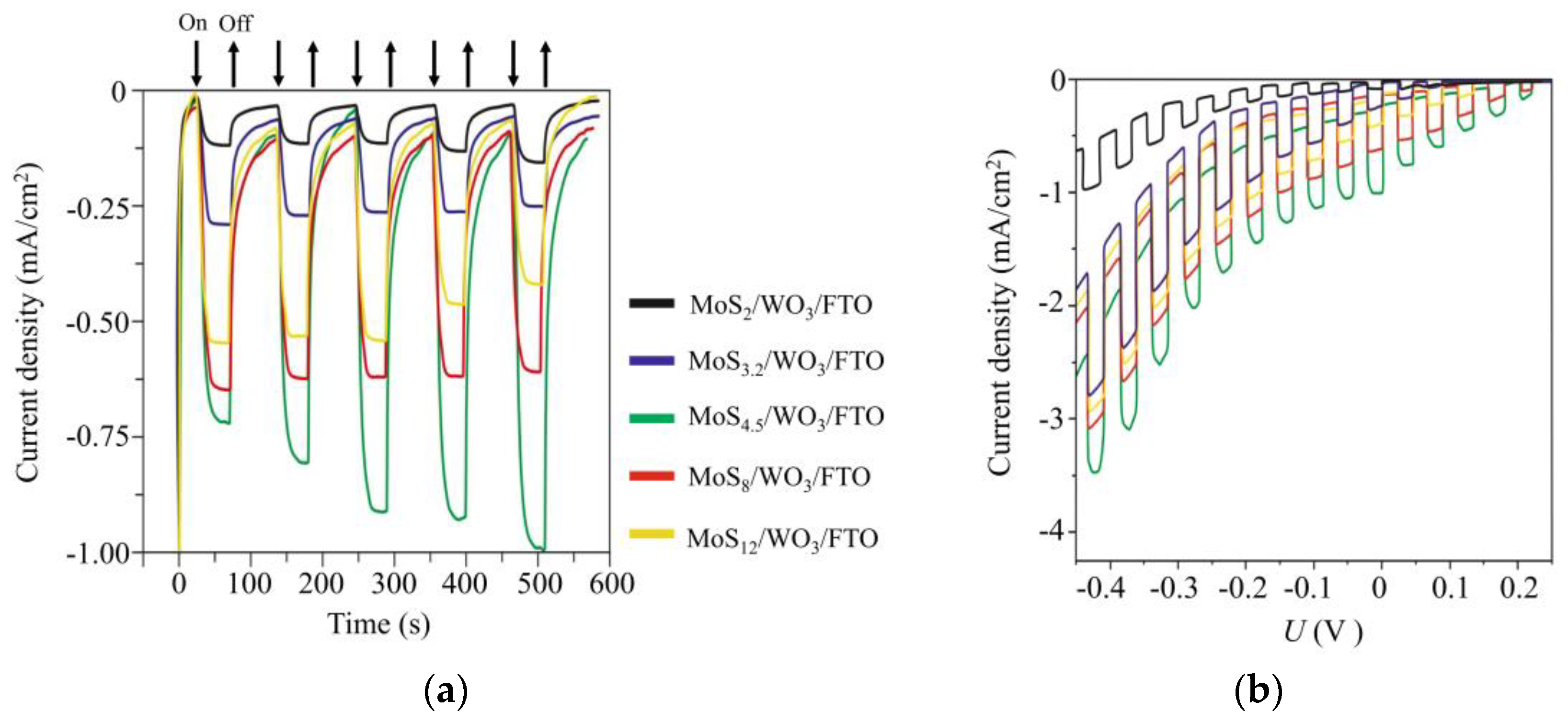
3.4. The Photoelectrocatalytical HER Performance of MoSx/WO3/FTO Samples

Figure 13 shows the chronoamperometry curves measured at an applied potential of ~0 V (RHE) under illumination, using chopped light for differently prepared MoSx/WO3/FTO samples. The highest photoelectrocatalytic activity was observed for the MoS4.5/WO3/FTO sample that contained a MoS4.5 film obtained by RPLD at an H2S pressure of 27 Pa. For this sample, the transient photocurrent response increased over time and reached ~1 mA/cm2 under illumination. This photocurrent value was maintained during measurements, the duration of which reached several days (Supplementary Materials Figure S8).
The thicknesses of the WO3 and MoS4.5 layers were ~250 and ~100 nm, respectively. It should be noted that we did not perform accurate optimization of the thickness of the MoSx films. Previously, we found that the deposition of thinner MoSx films caused a deterioration in photoelectrocatalytic HER performance of MoSx/WO3/FTO samples, and thicker MoSx films had poor transparency. The loading of the MoSx catalytic film was chosen so that MoSx/WO3/FTO samples absorbed only part of the photon flux (see Supplementary Materials Figure S9). Having passed through the photocathode, the light beam may be used to photoactivate the electrochemical process of OER on a photoanode, e.g., MoOz(S)/WO3/FTO, if it will have an appropriate optical property. To this end, the photoanode will be installed parallel to the photocathode and illuminated by the light passing through the photocathode.
An analysis of the efficiency of photoactivated HER dependence on the composition of MoSx films showed that this efficiency increased significantly with increasing sulfur concentration from x ~ 2 to x ~ 4.5. Then, the effectiveness of photoactivated HER decreased as sulfur concentration increased. RBS measurements showed that an increase in the concentration of sulfur in MoSx films was accompanied by an increase in its total content in the films. The growth rate of the photocurrent was, however, more substantial than the growth rate of the total amount of sulfur in the films. This could be due to the fact that, with increasing sulfur concentration, the proportion of sulfur atoms that were characterized by a high binding energy in the XPS spectra increased (Figure 7b). The increased catalytic activity of such sulfur atoms (bridging S22− and/or apical S2−) in the HER reaction is noted in [45]. A series of studies revealed the transformation of the structure and composition of amorphous MoSx≥3 catalysts during cathodic pretreatment [46,47,50]. It is assumed that the composition and states characteristic of MoS2 are formed in the surface layer of these catalysts. Excess sulfur is removed from the surface of MoSx≥3 catalysts in the form of H2S molecules. Obviously, with such a mechanism of the HER process, the surface density of catalytically active states should correlate with the content of Mo atoms in MoSx≥3 films. In our studies, for MoSx≥2 films, the total Mo content was approximately the same. The photoelectrocatalytic activity of MoSx/WO3/FTO samples increased, however, with growing sulfur content, until polysulfide clusters appeared in the films. Figure 13 also shows that the photocurrent increased with time for the MoS4.5/WO3/FTO sample but decreased for the films possessing larger S contents. This means that when the Mo content remains largely unchanged, the amount of sulfur affects stability and catalytic activity.

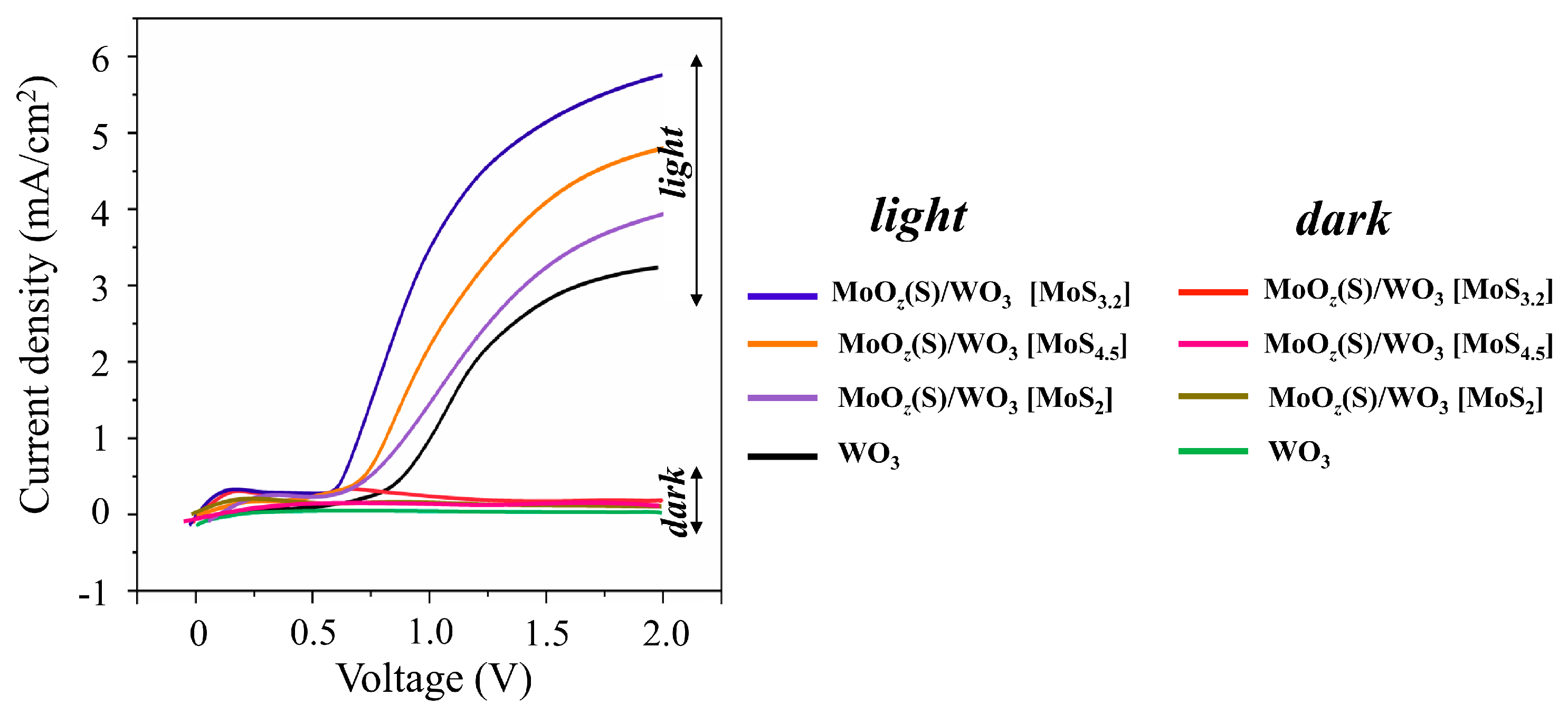
3.5. The Photoelectrocatalytical OER Performance of MoOz(S)/WO3/FTO Samples

Figure 14 shows LSV scans that were measured for WO3/FTO and different MoOz(S)/WO3/FTO samples without and under illumination by a Xe lamp. LSV curves for the WO3/FTO sample had a form characteristic of WO3-based photoanodes [38,39,42]. The photocurrent onset potential of the WO3/ FTO sample began at 0.8 V, and the photocurrent density increased steeply up to a plateau of about 2.9 mA/cm2 at 1.6 V. The received photocurrent for the WO3/FTO sample obtained by RPLD exceeded the photocurrent for WO3 films obtained by PLD by Mai et al. [38]. Comparison of WO3/FTO photoanodes obtained by RPLD in this work with WO3-based photoanodes obtained by various methods (see a review in [65]) indicates a rather high photoelectrochemical performance of WO3/FTO samples in O2 production by water splitting.
The formation of MoOz(S) films caused the modification of the OER performance of the WO3-containing photoanodes. The MoOz(S) films that were prepared by posttreatment of MoS3.2 precursors caused an almost twofold increase in the photocurrent (up to 5.3 mA/cm2 at 1.6 V) for the MoOz(S)/WO3/FTO sample compared to the photocurrent of the WO3/FTO sample. At the same time, the photocurrent onset potential decreased by about 0.2 V. The MoOz(S)/WO3/FTO photoanodes on the base of other MoSx precursors demonstrated the worse photoelectrochemical OER performances (Figure 14). The stability of the WO3/FTO and MoOz(S)/WO3/FTO photoanodes was measured under continuous illumination by a Xe lamp at a constant bias potential of 1.6 V (Supplementary Materials Figure S10). These measurements indicated that the MoOz(S) film did not cause a significant decrease in the stability of the photoanode during water splitting. After a fast drop in photocurrent at the beginning, the photocurrent slowly decreased for both photoanodes. The photocurrent remained ~70%–80% after 2 h illumination; this is typical of WO3-based photoanodes, as reported in [38,42].

4. Discussion

Comparison of the results obtained in this work with the findings of Fominski et al. [20] showed that regulating MoSx catalyst loading and improving the structural and chemical state of catalytic MoSx and photoactive WO3 layers helped to increase the efficiency of photoelectrochemical HER nearly tenfold when using a MoS4.5/WO3/FTO sample. As mentioned above, the chemical composition of the MoSx film was able to affect the efficiency of the photoelectrochemical process of HER. This happened when the chemical composition of a MoSx film had little effect on the structure of the energy bands of the latter. Figure 15 shows the assumed band structure of MoSx/WO3/FTO samples with different MoSx films. The position of energy bands in FTO was determined according to [66]. The MoSx films were selected that had a significant dependence between the efficiency of the photoelectrochemical HER process in MoSx/WO3/FTO samples, on the one hand, and the sulfur concentration, on the other. The results of VB-XPS studies for MoSx and WO3 thin films were used to determine the energy band structures. These results take into account the interactions between films (the built-in charge) on the interface. When removed from the interface, the upper edge of the valence band could move to the Fermi level in thicker MoSx films (see Supplementary Materials Figure S6).
The parameters of the band structures indicate that an increase in the sulfur concentration in MoSx films, from x ~ 2 to x ~ 4.5, could not cause significant changes in the mechanism of the photoelectrochemical process of HER. In all MoSx/WO3 heterostructures, this process followed the Z-scheme mechanism of charge separation and transfer (see Supplementary Materials Figure S11). Light absorption caused the generation of electron‒hole pairs in MoSx and WO3 films. The mutual position of energy bands in those films is such that the photogenerated electrons with strong reduction ability in the CB of MoSx film are preserved since the photogenerated holes in the VB of MoSx film and photogenerated electrons in the CB of WO3 with inferior redox power recombine. The redox power of the charge carriers are determined by the position of CB and VB energy levels relative to the HER and OER potentials, which are indicated in Figure 15. Photogenerated holes in the valence band of WO3 probably recombine with electrons (from the conduction band of FTO), which are injected from an external circuit. Due to such a direct Z-schema charge carrier transfer pathway, the electron lifetime may be increased in a MoSx catalyst film, and the flux of electrons with strong reduction ability to the MoSx/electrolyte interface will grow as a result. Although MoS2, MoS3.2, and MoS4.5 films did not differ in the type of conductivity, a lower concentration of equilibrium holes in MoS4.5 films was able to affect (i.e., reduce) the recombination rate of photogenerated electrons and holes in those films and thus to facilitate an increase in the electron flux to the surface of a MoS4.5 catalyst film. The concentration of photogenerated carriers in the MoS4.5 film may be the highest because the energy band gap of MoS4.5 is minimal in comparison with that of the MoS2 and MoS3.2 films (Figure 15). Even though the demonstrated photo-activated HER performance of RPLD MoSx/WOy heterostructures is lower compared to some previous studies of heterostructures that were prepared by PLD (e.g., CuBi2O4/NiO [67]), the thickness of the functional layers of obtained MoSx/WOy samples could be optimized to enhance their photoelectrocatalytic characteristics.
Figure 16 shows the results of a study into the energy band structures of MoOz(S)/WO3/FTO samples obtained by the anodic posttreatment of MoS3.2/WO3/FTO samples. The formation of a MoOz(S) film did not change the position of energy bands significantly. This position, however, is optimal for an efficient photoactivated OER process, which follows the traditional schema characteristic of Type II energy bands configuration (see Supplementary Materials Figure S12). Light absorption caused the generation of electron‒hole pairs in MoOz(S) and WO3 films. The preparation of the MoOz(S)/WO3 heterostructure made it possible to use the photogenerated holes in the MoOz(S) film quite efficiently, since the photogenerated in this film electrons sought to migrate into the WO3 film. The recombination of photogenerated electron‒hole pairs in MoOz(S) is slowed down due to migration of photogenerated electrons into the WO3 film. This is an energetically beneficial process since the lower edge of the conduction band in the latter film is below the lower edge of the conduction band in MoOz(S). Meanwhile, the photogenerated holes in these two semiconductors follow a reverse migration (see Supplementary Materials Figure S12). The WO3 film prevents a leakage of the photogenerated holes from MoOz(S) film into the WO3 film and provides an additional flux of the photogenerated in WO3 holes into the MoOz(S) film. Photogenerated holes move to MoOz(S) because of a higher energy of the upper edge of the valence band in MoOz(S). The holes accumulated in a MoOz(S) film can cause the enhanced efficiency of the OER process on the surface of MoOz(S)/WO3/FTO photoanode, provided the catalytic activity of the MoOz(S) film is higher than that of WO3.
It should be noted that the MoOz(S) film performs an important function, since it has a narrow energy band gap (~1.55 eV) and therefore effectively absorbs the Xe lamp radiation. For WO3 films with a moderate energy band gap (~2.7 eV), the theoretically achievable photocurrent density is ~4.5 mA/cm2 under AM1.5G illumination (100 mW/cm2) [15]. The use of an anodic semiconductor material with a narrow band gap allows this limit to be exceeded under several other conditions [68,69].
Note that the efficiency of MoOz(S)/WO3/FTO photoanodes depended on the composition of the initial MoSx precursor, which had undergone electrochemical posttreatment. The best properties were observed for the photoanodes obtained by post-treating MoS3.2/WO3/FTO samples. All the MoSx/WO3/FTO samples underwent anodic posttreatment in the same mode, which was determined by oxidation time and potential. Probably, obtaining efficient MoSx/WO3/FTO photoanodes requires each MoSx precursor to be post-treated differently.

5. Conclusions

Reactive PLD makes it possible to form consecutively nanostructured layers of the transition-metal oxide (WO3) and the transition-metal sulfide (MoSx) as well as to regulate their structural and chemical state by testing different substrate temperatures and reactive gas compositions and pressures. The optimization of the structural and chemical states of WO3 and MoSx thin films helps to obtain MoSx/WO3/FTO heterostructures on (FTO-coated) class substrates. Those structures have high efficiency in the photoelectrochemical process of HER in an acid solution. The best characteristics of photoactivated HER are associated with the samples that consist of porous nanocrystalline WO3 films (~250 nm thick) coated with porous amorphous MoS4.5 films (~100 nm thick) with a large effective area. On the MoS4.5/WO3/FTO photocathode, the HER photoelectrochemical process followed a Z-scheme mechanism, whereas the high efficiency of photoactivate HER was explained by an increased concentration of catalytically active states of sulfur. One cannot completely rule out the effect of sulfur concentration on the mechanisms of photoinduced charge transfer. In MoS4.5 films, the concentration of equilibrium holes, which could cause faster recombination with photogenerated electrons, was the lowest. The narrowest energy band gap of the MoS4.5 film facilitated the effective photogeneration of electron–hole pairs due to light absorption.
In MoSx/WO3/FTO heterostructures, MoSx films can be used as precursors to create effective MoOz(S)/WO3/FTO photoanodes for OER. To this end, it is important to select an optimal mode for the electrochemical posttreatment of MoSx films in order to obtain a MoOz(S) anodic material that is stable in an acid solution. A MoOz(S) film with relatively narrow energy band gap effectively absorbs light and ensures the migration of photogenerated holes to the surface of the MoOz(S)/WO3/FTO photoanode and causes OER to be catalyst-activated.

Supplementary Materials

The following are available online at https://www.mdpi.com/2079-4991/10/5/871/s1, Figure S1: RBS spectra for the WOy/FTO/glass samples. The WOy films were obtained by RPLD at different pressures of dry air, Figure S2: SEM images of the WOy films which were obtained in this work by reactive PLD at dry air pressures of (a) 20 and (b) 60 Pa. The temperature of the FTO substrate was 420 °C, Figure S3: VB-XPS spectrum of the WO3 film obtained by RPLD at a dry air pressure of 40 Pa, Figure S4: XPS Mo 3d and S 2p spectra for MoSx films, which were obtained by RPLD at different pressures of H2S gas, Figure S5: Tauc plots for the (a) MoS2 and (b) MoS3.2 films, Figure S6: VB-XPS spectra of relatively thick (a) MoS2, (b) MoS3.2, and (c) MoS4.5 films, Figure S7: (a) Tauc plot and (b) the leading edge of VB-XPS spectrum for thin MoOz(S) film, which was obtained on WO3 by electrochemical oxidation of precursor MoS3.2 film, Figure S8: Chronoamperometry stability measurement under chopped illumination of Xe lamp for the MoS4.5/WO3/FTO photocathode in 0.5 M H2SO4 solution at a potential of 0 V (RHE), Figure S9: Transmittance of the MoS4.5/WO3/FTO sample, Figure S10: Transient voltammogram of WO3/FTO and MoOz(S)/WO3/FTO photoanodes measured under a Xe lamp illumination at an applied potential of 1.6 V (RHE), Figure S11: The mechanism (Z-schema) of the photo-activated electrochemical process of HER (including the suggested mechanism of charge carrier transport) for the MoSx/WO3/FTO heterostructure. Band gaps and band edge positions for the heterostructure are shown, Figure S12: The mechanism of the photo-activated electrochemical process of OER (including the suggested mechanism of charge carrier transport) for the MoOz(S)/WO3/FTO heterostructure. Band gaps and band edge positions for the heterostructure are shown.

Author Contributions

Conceptualization and writing—original draft preparation, V.F.; methodology, M.D. and A.G.; validation, R.R.; investigation, D.F., A.S., O.R., K.M., and P.S. All authors have read and agreed to the published version of the manuscript.

Funding

This research was funded by the Russian Science Foundation, grant number 19-19-00081. Sample characterization by Rutherford backscattering spectroscopy of ions and Raman spectroscopy has been done in REC “Functional Nanomaterials” with support from Ministry of Science and Higher Education of the Russian Federation (project FZWN-2020-0008).

Conflicts of Interest

The authors declare no conflicts of interest.

References

  1. Haque, F.; Daeneke, T.; Kalantar-zadeh, K.; Zhen-Ou, J. Two-Dimensional Transition Metal Oxide and Chalcogenide-Based Photocatalysts. Nano Micro Lett. 2018, 10, 23. [Google Scholar] [CrossRef] [PubMed] [Green Version]
  2. Ouyang, T.; Ye, Y.; Wu, C.; Xiao, K.; Liu, Z. Heterostructures Composed of N-Doped Carbon Nanotubes Encapsulating Cobalt and β-Mo2C Nanoparticles as Bifunctional Electrodes for Water Splitting. Angew. Chem. Int. Ed. 2018, 58, 15. [Google Scholar] [CrossRef]
  3. Di, L.; Yang, H.; Xian, T.; Liu, X.; Chen, X. Photocatalytic and Photo-Fenton Catalytic Degradation Activities of Z-Scheme Ag2S/BiFeO3 Heterojunction Composites under Visible-Light Irradiation. Nanomaterials 2019, 9, 399. [Google Scholar] [CrossRef] [PubMed] [Green Version]
  4. Shi, C.; Zhou, X.; Li, W.; Guo, H.; Zhao, Y.; Ruan, L.; Xu, C.; Zeng, W.; Liang, D. Synergistic enhancing photoelectrochemical response of Bi10O6S9 with WO3 optical heterojunction in wide wavelength range. Appl. Surf. Sci. 2020, 509, 144697. [Google Scholar] [CrossRef]
  5. Jiaa, J.; Jiangb, C.; Zhanga, X.; Lia, P.; Xionga, J.; Zhanga, Z.; Wua, T.; Wang, Y. Urea-modified carbon quantum dots as electron mediator decorated g-C3N4/WO3 with enhanced visible-light photocatalytic activity and mechanism insight. Appl. Surf. Sci. 2019, 495, 143524. [Google Scholar] [CrossRef]
  6. Zhang, H.; Ding, Q.; He, D.; Liu, H.; Liu, W.; Li, Z.; Yang, B.; Zhang, X.; Lei, L.; Jin, S. A p-Si/NiCoSex core/shell nanopillar array photocathode for enhanced photoelectrochemical hydrogen production. Energy Environ. Sci. 2016, 9, 3113–3119. [Google Scholar] [CrossRef]
  7. Zhu, D.; Wang, X.; An, H.; Zhong, Y.; Wang, D.; Tang, C.; Hu, C. Facile One-Step Hydrothermal Fabrication of (Sr0.6Bi0.305)2Bi2O7/SnO2 Heterojunction with Excellent Photocatalytic Activity. Nanomaterials 2020, 10, 321. [Google Scholar] [CrossRef] [Green Version]
  8. He, F.; Meng, A.; Chengm, B.; Hob, W.; Yu, J. Enhanced photocatalytic H2-production activity of WO3/TiO2 step-scheme heterojunction by graphene modification. Chin. J. Catal. 2020, 41, 9–20. [Google Scholar] [CrossRef]
  9. Zhang, L.; Hao, X.; Li, Y.; Jin, Z. Performance of WO3/g-C3N4 heterojunction composite boosting with NiS for photocatalytic hydrogen evolution. Appl. Surf. Sci. 2020, 499, 143862. [Google Scholar] [CrossRef]
  10. Gao, C.; Yu, H.; Zhang, L.; Zhao, Y.; Xie, J.; Li, C.; Cui, K.; Yu, J. Ultrasensitive Paper-Based Photoelectrochemical Sensing Platform Enabled by the Polar Charge Carriers-Created Electric Field. Anal. Chem. 2020, 92, 2902–2906. [Google Scholar] [CrossRef] [Green Version]
  11. Jadwiszczak, M.; Jakubow-Piotrowska, K.; Kedzierzawski, P.; Bienkowski, K.; Augustynski, J. Highly Efficient Sunlight-Driven Seawater Splitting in a Photoelectrochemical Cell with Chlorine Evolved at Nanostructured WO3 Photoanode and Hydrogen Stored as Hydride within Metallic Cathode. Adv. Energy Mater. 2019, 10, 3. [Google Scholar] [CrossRef]
  12. Rassoolkhani, A.; Cheng, W.; Lee, J.; McKee, A.; Koonce, J.; Coffel, J.; Ghanim, A.; Aurand, G.; Kim, C.; Park, W.; et al. Nanostructured bismuth vanadate/tungsten oxide photoanode for chlorine production with hydrogen generation at the dark cathode. Commun. Chem. 2019, 2, 57. [Google Scholar] [CrossRef] [Green Version]
  13. Coridan, R.; Shaner, M.; Wiggenhorn, C.; Brunschwig, D.; Lewis, N. Electrical and Photoelectrochemical Properties of WO3/Si Tandem Photoelectrodes. J. Phys. Chem. 2013, 117, 14–6949. [Google Scholar] [CrossRef] [Green Version]
  14. Liu, X.; Zhou, H.; Pei, S.; Xiea, S.; You, S. Oxygen-deficient WO3−x nanoplate array film photoanode for efficient photoelectrocatalytic water decontamination. Chem. Eng. J. 2020, 381, 122740. [Google Scholar] [CrossRef]
  15. Shina, S.; Hana, H.S.; Kim, J.S.; Park, I.K.; Lee, M.H.; Hong, K.S.; Cho, I.S. Tree-like Nanoporous WO3 Photoanode with Enhanced Charge Transport Efficiency for Photoelectrochemical Water Oxidation. J. Mater. Chem. A 2015, 3, 12920–12926. [Google Scholar] [CrossRef]
  16. Murcia-López, S.; Fàbrega, C.; Monllor-Satoca, D.; Hernández-Alonso, M.D.; Penelas-Pérez, G.; Morata, A.; Morante, J.R.; Andreu, T. Tailoring Multilayered BiVO4 Photoanodes by Pulsed Laser Deposition for Water Splitting. ACS Appl. Mater. Interfaces 2016, 8, 4076–4085. [Google Scholar] [CrossRef]
  17. Kölbach, M.; Harbauer, K.; Ellmer, K.; Krol, R. Elucidating the Pulsed Laser Deposition Process of BiVO4 Photoelectrodes for Solar Water Splitting. J. Phys. Chem. C 2020, 124, 4438–4447. [Google Scholar] [CrossRef]
  18. Liu, Y.; Wygant, B.; Mabayoje, O.; Lin, J.; Kawashima, K.; Kim, J.; Li, W.; Li, J.; Mullins, C. Interface Engineering and its Effect on WO3-Based Photoanode and Tandem Cell. ACS Appl. Mater. Interfaces 2018, 10, 12639–12650. [Google Scholar] [CrossRef]
  19. Hu, G.; Li, J.; Liu, P.; Zhu, X.; Li, X.; Nauman Ali, R.; Xiang, B. Enhanced electrocatalytic activity of WO3@NPRGO composite in a hydrogen evolution reaction. Appl. Surf. Sci. 2019, 463, 275–282. [Google Scholar] [CrossRef]
  20. Fominski, V.; Gnedovets, A.; Fominski, D.; Romanov, R.; Kartsev, P.; Rubinkovskaya, O.; Novikov, S. Pulsed Laser Deposition of Nanostructured MoS3/np-Mo//WO3−y Hybrid Catalyst for Enhanced (Photo) Electrochemical Hydrogen Evolution. Nanomaterials 2019, 9, 1395. [Google Scholar] [CrossRef] [Green Version]
  21. Yao, J.; Zhang, M.; Yin, H.; Luo, Y.; Liu, X. Improved photocatalytic activity of WO3/C3N4: By constructing an anchoring morphology with a Z-scheme band structure. Solid State Sci. 2019, 95, 105926. [Google Scholar] [CrossRef]
  22. Nevolin, V.N.; Grigoriev, S.N.; Fominski, V.Yu.; Romanov, R.I.; Volosova, M.A.; Fominski, D.V.; Dzhumaev, P.S. Application of pulsed laser deposition in reactive gaseous media to fabricate an effective hybrid MoSx/WOy catalyst for the reaction of hydrogen evolution. Inorg. Mater. Appl. Res. 2018, 9, 297–304. [Google Scholar] [CrossRef]
  23. He, K.; Xie, J.; Luo, X.; Wen, J.; Ma, S.; Li, X.; Fang, Y.; Zhang, X. Enhanced visible light photocatalytic H2 production over Z-scheme g-C3N4 nansheets/WO3 nanorods nanocomposites loaded with Ni(OH)x cocatalysts. Chin. J. Catal. 2017, 38, 240–252. [Google Scholar] [CrossRef]
  24. Hou, Y.; Zuo, F.; Dagg, A.P.; Liu, J.; Feng, P. Branched WO3 nanosheet array with layered C3N4 heterojunctions and CoOx nanoparticles as a flexible photoanode for efficient photoelectrochemical water oxidation. Adv. Mater. 2014, 26, 5043–5049. [Google Scholar] [CrossRef] [PubMed]
  25. Chai, B.; Liu, C.; Yan, J.; Ren, Z.; Wang, Z.J. In-situ synthesis of WO3 nanoplates anchored on g-C3N4 Z-scheme photocatalysts for significantly enhanced photocatalytic activity. Appl. Surf. Sci. 2018, 448, 1–8. [Google Scholar] [CrossRef]
  26. Fominski, V.; Romanov, R.; Fominski, D.; Shelyakov, A. Regulated growth of quasi-amorphous MoSx thin-film hydrogen evolution catalysts by pulsed laser deposition of Mo in reactive H2S gas. Thin Solid Films 2017, 642, 58–68. [Google Scholar] [CrossRef]
  27. Zafir, M.; Nasir, M.; Sofer, Z.; Ambrosia, A.; Pumera, M. A limited anodic and cathodic potential window of MoS2: Limitations in electrochemical applications. Nanoscale 2015, 7, 3126–3129. [Google Scholar] [CrossRef]
  28. Inzani, K.; Nematollahi, M.; Vullum-Bruer, F.; Grande, T.; Reenaas, T.; Selbach, S. Electronic properties of reduced molybdenum oxides. Phys. Chem. Chem. Phys. 2017, 19, 9232–9245. [Google Scholar] [CrossRef]
  29. Ohtsuka, H.; Sakurai, Y. Characterization of MoO3−x Thin Films. Jpn. J. Appl. Phys. 2001, 40, 4680–4683. [Google Scholar] [CrossRef]
  30. Schmidt, E.; Sourisseau, C.; Meunier, G.; Levasseur, A. Amorphous molybdenum oxysulfide thin films and their physical characterization. Thin Solid Films 1995, 260, 21–25. [Google Scholar] [CrossRef]
  31. Bao, X.-Q.; Petroykh, D.; Alpuim, P.; Stroppa, D.G.; Guldris, N.; Fonseca, H.; Costa, M.; Gaspar, J.; Jin, C.; Liu, L. Amorphous oxygen-rich molybdenum oxysulfide Decorated p-type silicon microwire arrays for efficient photoelectrochemical water reduction. Nano Energy 2015, 16, 130–142. [Google Scholar] [CrossRef]
  32. Kraut, E.A.; Grant, R.W.; Waldrop, J.R.; Kowalczuk, S.P. Precise Determination of the Valence-Band Edge in X-Ray Photoemission Spectra: Application to Measurement of Semiconductors Interface Potentials. Phys. Rev. Lett. 1980, 44, 1620. [Google Scholar] [CrossRef]
  33. Chiu, M.-H.; Zhang, C.; Shiu, H.-W.; Chuu, C.-P.; Chen, C.-H.; Chang, C.-Y.S.; Chen, C.-H.; Chou, M.-Y.; Shih, C.-K.; Li, L.-J. Determination of band alignment in the single-layer MoS2/WSe2 heterojunction. Nat. Commun. 2015, 6, 7666. [Google Scholar] [CrossRef] [PubMed] [Green Version]
  34. Romanov, R.I.; Slavich, A.S.; Kozodaev, M.G.; Myakota, D.I.; Lebedinskii, Yu. Yu.; Novikov, S.M.; Markeev, A.M. Band alignment in as-transferred and annealed graphene/MoS2 heterostructures. Phys. Status Solidi RRL 2019. [Google Scholar] [CrossRef]
  35. Pierucci, D.; Henck, H.; Avila, J.; Balan, A.; Naylor, C.H.; Patriarche, G.; Dappe, Y.J.; Silly, M.G.; Sirotti, F.; Johnson, A.T.C.; et al. Band Alignment and Minigaps in Monolayer MoS2-Graphene van der Waals Heterostructures. Nano Lett. 2016, 16, 4054. [Google Scholar] [CrossRef]
  36. Xu, L.; Yin, M.L.; Liu, S.F. Agx@WO3 core-shell nanostructure for LSP enhanced chemical sensors. Sci. Rep. 2014, 4, 45. [Google Scholar] [CrossRef] [Green Version]
  37. Chen, S.; Xiao, Y.; Xie, W.; Wang, Y.; Hu, Z.; Zhang, W.; Zhao, H. Facile Strategy for Synthesizing Non-Stoichiometric Monoclinic Structured Tungsten Trioxide (WO3−x) with Plasma Resonance Absorption and Enhanced Photocatalytic Activity. Nanomaterials 2018, 8, 553. [Google Scholar] [CrossRef] [Green Version]
  38. Mai, M.; Ma, X.; Zhou, H.; Ye, M.; Li, T.; Ke, S.; Lin, P.; Zeng, X. Effect of oxygen pressure on pulsed laser deposited WO3 thin films for photoelectrochemical water splitting. J. Alloys Compd. 2017, 722, 913–919. [Google Scholar] [CrossRef]
  39. Zhan, F.; Liu, Y.; Wang, K.; Liu, Y.; Yang, X.; Yang, Y.; Qiu, X.; Li, W.; Li, J. In Situ Formation of WO3-Based Heterojunction Photoanodes with Abundant Oxygen Vacancies via a Novel Microbattery Method. ACS Appl. Mater. Interfaces 2019, 11, 15467–15477. [Google Scholar] [CrossRef]
  40. Fominski, V.; Romanov, R.; Zuev, V.; Soloviev, A.; Goikhman, A.; Maksimova, K.; Shvets, P.; Demin, M. Comparison of hydrogen detection by WOx/SiC and Pt/WOx/SiC structures using amperometric and potentiometric modes of measurement. Thin Sold Films 2019, 669, 461–470. [Google Scholar] [CrossRef]
  41. Fominski, V.Y.; Grigoriev, S.N.; Romanov, R.I.; Volosova, M.A.; Fominski, D.V.; Irzhak, A.V. Structure, morphology and electrocatalytic properties of WOx thin films prepared by reactive pulsed laser deposition. J. Phys. Conf. Ser. 2017, 941, 012062. [Google Scholar] [CrossRef]
  42. Kalanur, S.S. Structural, Optical, Band Edge and Enhanced Photoelectrochemical Water Splitting Properties of Tin-Doped WO3. Catalysts 2019, 9, 456. [Google Scholar] [CrossRef] [Green Version]
  43. Zhan, F.; Yang, Y.; Li, W.; Li, J.; Liu, W.; Li, Y.; Chena, Q. Preparation of DyVO4/WO3 heterojunction plate array films with enhanced photoelectrochemical activity. RSC Adv. 2016, 6, 1039. [Google Scholar] [CrossRef]
  44. Grigoriev, S.N.; Fominski, V.Y.; Romanov, R.I.; Gnedovets, A.G.; Volosova, M.A. Shadow masked pulsed laser deposition of WSex films: Experiment and modeling. Appl. Surf. Sci. 2013, 282, 607–614. [Google Scholar] [CrossRef]
  45. Lee, C.-H.; Lee, S.; Lee, Y.-K.; Jung, Y.C.; Ko, Y.-I.; Lee, D.C.; Joh, H.-I. Understanding on the origin of formation and active sites for thiomolybdate [Mo3S13]2− clusters as hydrogen-evolution catalyst through the selective control of sulfur atoms. ACS Catal. 2018, 8, 5221–5227. [Google Scholar] [CrossRef]
  46. Deng, Y.; Ting, L.R.L.; Neo, P.H.L.; Zhang, Y.-J.; Peterson, A.A.; Yeo, B.S. Operando Raman spectroscopy of amorphous molybdenum sulfide (MoSx) during the electrochemical hydrogen evolution reaction: Identification of sulfur atoms as catalytically active sites for H+ reduction. ACS Catal. 2016, 6, 7790–7798. [Google Scholar] [CrossRef]
  47. Lassalle-Kaiser, B.; Merki, D.; Vrubel, H.; Gul, S.; Yachandra, V.K.; Hu, X.; Yano, J. Evidence from in situ X-ray absorption spectroscopy for the involvement of terminal disulfide in the reduction of protons by an amorphous molybdenum sulfide electrocatalyst. J. Am. Chem. Soc. 2015, 137, 314–321. [Google Scholar] [CrossRef] [Green Version]
  48. Hibble, S.J.; Rice, D.A.; Pickup, D.M.; Beer, M.P. Mo K-edge EXAFS and S K-edge absorption studies of the amorphous molybdenum sulfides MoS4.7, MoS3, and MoS3nH2O (n~2). Inorg. Chem. 1995, 34, 5109–5113. [Google Scholar] [CrossRef]
  49. Hibble, S.J.; Wood, G.B. Modeling the structure of amorphous MoS3: A neutron diffraction and reverse Monte Carlo study. J. Am. Chem. Soc. 2004, 126, 959–965. [Google Scholar] [CrossRef]
  50. Xi, F.; Bogdanoff, P.; Harbauer, K.; Plate, P.; Höhn, C.; Rappich, J.; Wang, B.; Han, X.; van de Krol, R.; Fiechter, S. Structural transformation identification of sputtered amorphous MoSx as efficient hydrogen evolving catalyst during electrochemical activation. ACS Catal. 2019, 9, 2368–2380. [Google Scholar] [CrossRef]
  51. Müller, A.; Jostes, R.; Jaegermann, W.; Bhattacharyya, R. Spectroscopic investigation on the molecular and electronic structure of [Mo3S13]2−, a discrete binary transition metal sulfur cluster. Inorg. Chim. Acta 1980, 41, 259–263. [Google Scholar] [CrossRef]
  52. Weber, Th.; Muijsers, J.C.; Niemantsverdriet, J.W. Structure of amorphous MoS3. J. Phys. Chem. 1995, 99, 9194–9200. [Google Scholar] [CrossRef] [Green Version]
  53. Fominski, V. Yu.; Markeev, A.M.; Nevolin, V.N.; Prokopenko, V.B.; Vrublevski, A.R. Pulsed laser deposition of MoSx films in a buffer gas atmosphere. Thin Solid Films 1994, 248, 240–246. [Google Scholar] [CrossRef]
  54. Cao, Y.; Shin, Y.C. Multi-scale modeling of phase explosion in high fluence nanosecondlaser ablation and clarification of ablation depth prediction criterion. Appl. Surf. Sci. 2015, 357, 74–85. [Google Scholar] [CrossRef] [Green Version]
  55. Bennett, T.D.; Grigoropoulos, C.P.; Krajnovich, D.J. Near-threshold laser sputtering of gold. J. Appl. Phys. 1995, 77, 849–864. [Google Scholar] [CrossRef]
  56. Fominski, V.Yu.; Grigoriev, S.N.; Gnedovets, A.G.; Romanov, R.I. On the Mechanism of Encapsulated Particle Formation during Pulsed Laser Deposition of WSex Thin-Film Coatings. Technic. Phys. Lett. 2013, 39, 312–315. [Google Scholar] [CrossRef]
  57. Fominski, V.Yu.; Romanov, R.I.; Nevolin, V.N.; Fominski, D.V.; Komleva, O.V.; Popov, V.V. Formation of ultrathin MoS2 films using laser-based methods. J. Phys. Conf. Ser. 2019, 1238, 012007. [Google Scholar] [CrossRef] [Green Version]
  58. Escalera-López, D.; Lou, Z.; Rees, N.V. Benchmarking the activity, stability, and inherent electrochemistry of amorphous molybdenum sulfide for hydrogen production. Adv. Energy Mater. 2019, 9, 1802614. [Google Scholar] [CrossRef]
  59. Benoist, L.; Gonbeau, D.; Pfister-Guillouze, G.; Schmidt, E.; Meunier, G.; Levasseur, A. X-ray photoelectron spectroscopy characterization of amorphous molybdenum oxysulfide thin films. Thin Solid Films 1995, 258, 110–114. [Google Scholar] [CrossRef]
  60. Escalera-López, D.; Niu, Y.; Park, S.J.; Isaacs, M.; Wilson, K.; Palmer, R.E.; Rees, N.V. Hydrogen evolution enhancement of ultra-low loading, size-selected molybdenum sulfide nanoclusters by sulfur enrichment. Appl. Catal. B Environ. 2018, 235, 84–91. [Google Scholar] [CrossRef]
  61. King, L.A.; Hellstern, T.R.; Park, J.; Sinclair, R.; Jaramillo, T.F. Highly Stable Molybdenum Disulfide Protected Silicon Photocathodes for Photoelectrochemical Water Splitting. ACS Appl. Mater. Interfaces 2017, 9, 36792–36798. [Google Scholar] [CrossRef] [PubMed]
  62. Olofinjana, B.; Egharevba, G.O.; Eleruja, M.A.; Jeynes, C.; Adedeji, A.V.; Akinwunmi, O.O.; Taleatu, B.A.; Mordi, C.U.; Ajayi, E.O.B. Synthesis and Some Properties of Metal Organic Chemical Vapour Deposited Molybdenum Oxysulphide Thin Films. J. Mater. Sci. Technol. 2010, 26, 552–557. [Google Scholar] [CrossRef]
  63. Butler, K.Y.; Crespo-Otero, R.; Buckeridge, J.; Scanlon, D.O.; Bovill, E.; Lidzey, D.; Walsh, A. Band energy control of molybdenum oxide by surface hydration. Appl. Phys. Lett. 2015, 107, 231605. [Google Scholar] [CrossRef]
  64. Qin, P.; Fang, G.; Cheng, F.; Ke, W.; Lei, H.; Wang, H.; Zhao, X. Sulfur-Doped Molybdenum Oxide Anode Interface Layer for Organic Solar Cell Application. ACS Appl. Mater. Interfaces 2014, 6, 2963–2973. [Google Scholar] [CrossRef] [PubMed]
  65. Kalanur, S.S.; Duy, L.T.; Seo, H. Recent Progress in Photoelectrochemical Water Splitting Activity of WO3 Photoanodes. Top. Catal. 2018, 61, 1043–1076. [Google Scholar] [CrossRef]
  66. Saha, B.; Sarkar, K.; Bera, A.; Deb, K.; Thapa, R. Schottky diode behaviour with excellent photoresponse in NiO/FTO heterostructure. Appl. Surf. Sci. 2017, 418, 328–334. [Google Scholar] [CrossRef]
  67. Lee, J.; Yoon, H.; Kim, S.; Seo, S.; Song, J.; Choi, B.U.; Choi, S.Y.; Park, H.; Ryu, S.; Oh, J.; et al. Long-term stabilized high-density CuBi2O4/NiO heterostructure thin film photocathode grown by pulsed laser deposition. Chem. Commun. 2019, 55, 12447. [Google Scholar] [CrossRef]
  68. Li, C.; Cao, Q.; Wang, F.; Xiao, Y.; Li, Y.; Delaunay, J.J.; Zhu, H. Engineering graphene and TMDs based van der Waals heterostructures for photovoltaic and photoelectrochemical solar energy conversion. Chem. Soc. Rev. 2018, 47, 4981–5037. [Google Scholar] [CrossRef]
  69. Hu, S.; Xiang, C.; Haussener, S.; Bergercd, A.D.; Lewis, N.S. An analysis of the optimal band gaps of light absorbers in integrated tandem photoelectrochemical water-splitting systems. Energy Environ. Sci. 2013, 6, 2984–2993. [Google Scholar] [CrossRef] [Green Version]
Figure 1. Experimental (a) RBS and (b) Raman spectra for the WOy films obtained on an FTO substrate by RPLD at different pressures of dry air.
Nanomaterials 10 00871 g001
Figure 2. XPS (a) W 4f and (b) O 1s spectra for the surface of WOy film, which was obtained by RPLD at a dry air pressure of 40 Pa.
Nanomaterials 10 00871 g002
Figure 3. XRD pattern for WO3 film obtained on an FTO substrate by RPLD at a dry air pressure of 40 Pa.
Nanomaterials 10 00871 g003
Figure 4. SEM images with two magnifications for a WO3 film obtained on an FTO substrate by RPLD at a dry air pressure of 40 Pa.
Nanomaterials 10 00871 g004
Figure 5. (a) UV–visible absorption spectra and (b) Tauc plot of a WO3 film obtained on FTO substrate by RPLD at a dry air pressure of 40 Pa.
Nanomaterials 10 00871 g005
Figure 6. (a) The RBS spectrum for MoSx film obtained by RPLD on a Si substrate at an H2S pressure of 27 Pa; (b) deposition rates and compositions of MoSx films obtained by RPLD at different pressures of H2S gas.
Nanomaterials 10 00871 g006
Figure 7. (a) The XPS Mo 3d and S 2p spectra for a MoS4.5 film obtained by RPLD at an H2S pressure of 27 Pa; (b) the relative content of low binding energy (LBE), high binding energy (HBE), and S0 states of sulfur atoms in MoSx films obtained by RPLD at different pressures of H2S gas.
Nanomaterials 10 00871 g007
Figure 8. (a) TEM image and selected area diffraction (SAED) patterns of the thin MoS4.5 film obtained by RPLD (the local area of the film that contained Mo particles was selected). The bottom insert shows high-resolution TEM image of the MoS4.5 film. (b) Typical TEM image of the MoS4.5 film, which indicates a low content of Mo particles embedded in this film.
Nanomaterials 10 00871 g008
Figure 9. Raman spectra for different MoSx films obtained by RPLD. The insert shows terminal (S22−t), bridging (S22−b), and apical (S2−ap) ligands in a 3Mo‒S (Mo3S13) cluster.
Nanomaterials 10 00871 g009
Figure 10. (a) UV–visible absorption spectra and (b) Tauc plot of MoS4.5 film.
Nanomaterials 10 00871 g010
Figure 11. The (a) planar and (b) cross-section SEM images of the MoS4.5/WO3/FTO sample.
Nanomaterials 10 00871 g011
Figure 12. The XPS (a) Mo 3d and (b) S 2p spectra for a MoS3.2 film obtained by RPLD at an H2S pressure of 18 Pa and post-treated in acidic solution at a potential of 2 V.
Nanomaterials 10 00871 g012
Figure 13. (a) Chopped (light/dark) chronoamperometry curves and (b) chopped linear sweep voltammetry (LSV) curves of MoSx/WO3/FTO photocathodes with a different stoichiometry of MoSx catalytic films. The curves were measured in a 0.5 H2SO4 solution at an applied potential of ~0 V (RHE) under Xe lamp illumination (~100 mW/cm2).
Nanomaterials 10 00871 g013
Figure 14. The LSV curves of WO3/FTO and different MoOz(S)/WO3/FTO samples measured in the dark and under illumination by a Xe lamp in 0.5 M H2SO4. The MoOz(S) films were prepared by posttreatment of MoSx precursors with different content of S atoms (indicated in square brackets).
Nanomaterials 10 00871 g014
Figure 15. The proposed energy band diagrams for MoS2/WO3/FTO, MoS3.2/WO3/FTO, and MoS4.5/WO3/FTO samples. The schema represents the band offsets between WO3 with thin MoSx films. CB and VB indicate the conduction band and valence band, respectively.
Nanomaterials 10 00871 g015
Figure 16. The proposed energy band diagram for MoOz(S)/WO3/FTO sample. The schema represents band offset between WO3 with a thin MoOz(S) film. CB and VB indicate the conduction band and valence band, respectively.
Nanomaterials 10 00871 g016

