Direct Patterned Zinc-Tin-Oxide for Solution-Processed Thin-Film Transistors and Complementary Inverter through Electrohydrodynamic Jet Printing

 , , and
Abstract
:1. Introduction
2. Materials and Methods
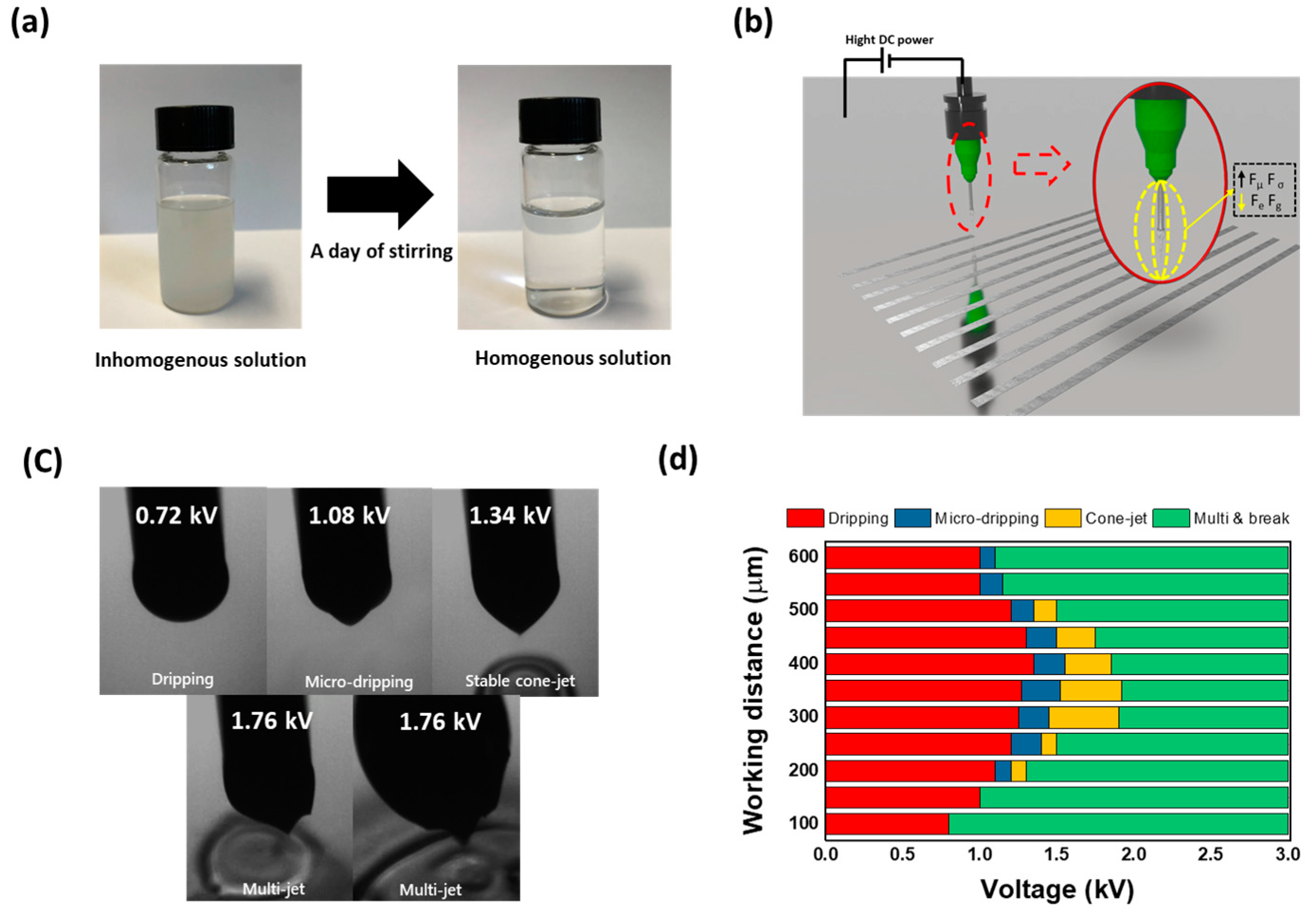
2.1. Materials and Sample Preparation
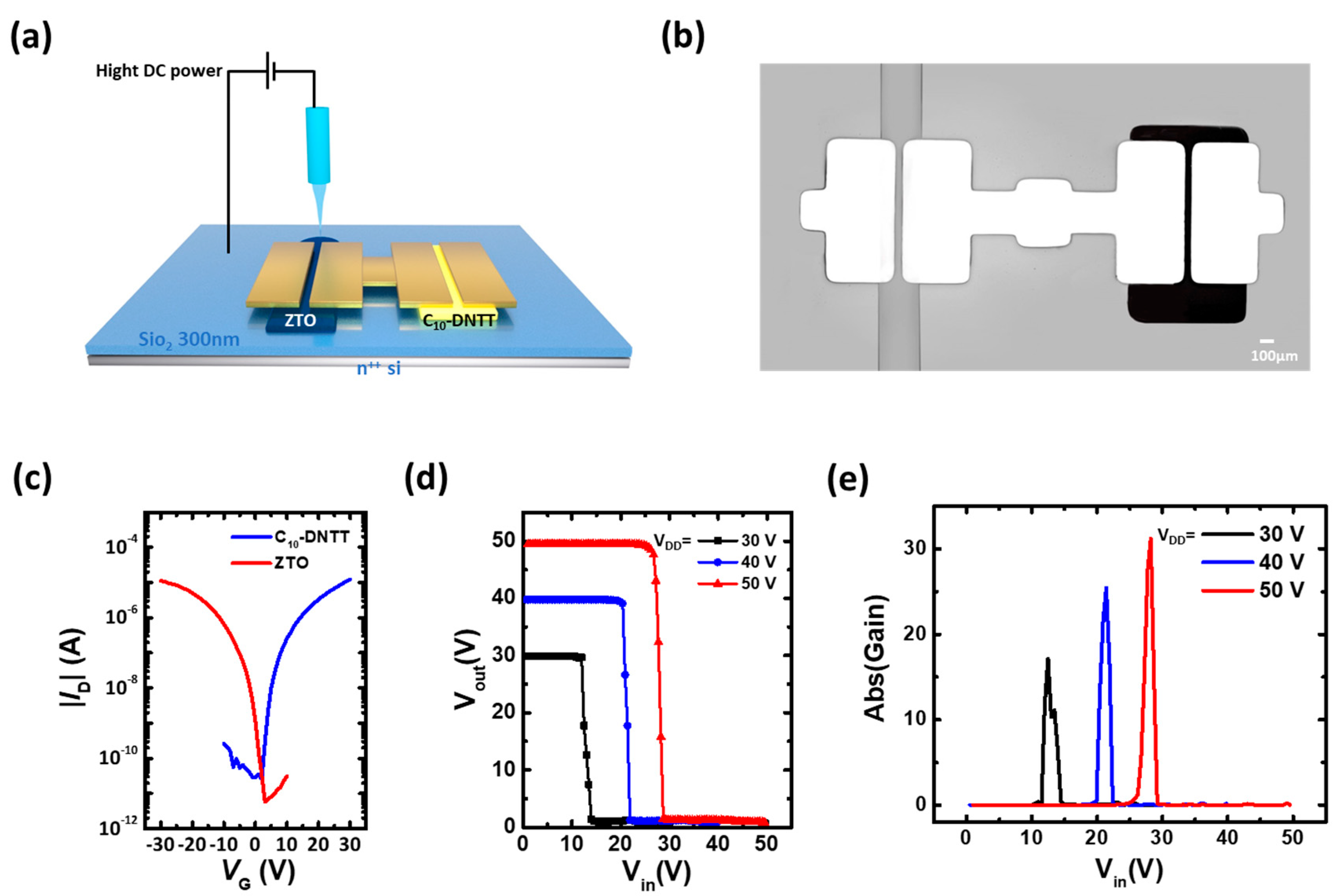
2.2. Fabrication of ZTO Patterning and Solution-Processed Oxide TFTs
2.3. Fabrication of Complementary Inverters
2.4. Characterization
3. Results and Discussion
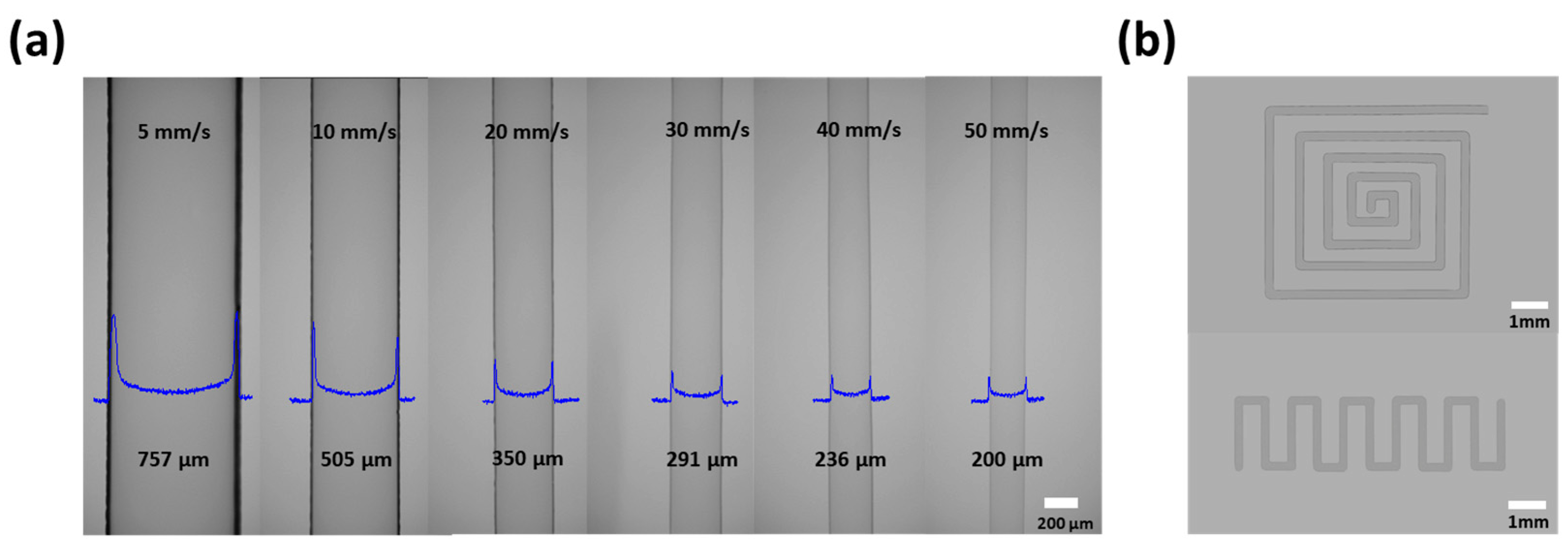
3.1. Patterning of EHD Jet-Printed ZTO Layers
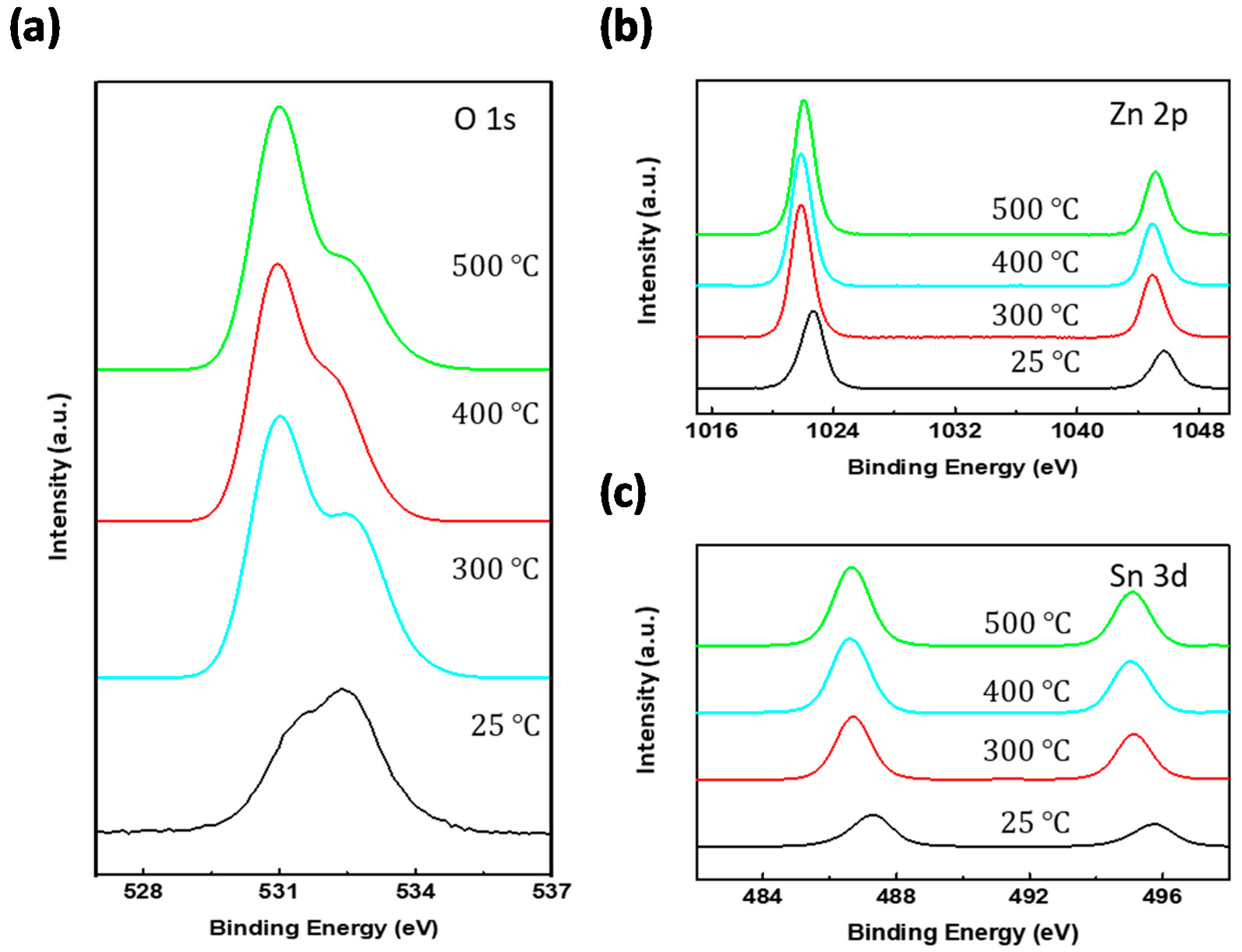
3.2. ZTO Active Layer Fabrication
3.3. ZTO Active and MWCNT S/D-Based TFT
4. Conclusions
Supplementary Materials
Author Contributions
Funding
Conflicts of Interest
References
- Han, C.-W.; Park, J.; Choi, H.-S.; Kim, T.-S.; Shin, Y.-H.; Shin, H.-J.; Lim, M.-J.; Kim, B.-C.; Kim, H.-S.; Kim, B.-S.; et al. Advanced technologies for UHD curved OLED TV. J. Soc. Inf. Disp. 2014, 22, 552–563. [Google Scholar] [CrossRef]
- Marinkovic, M.; Takata, R.; Neumann, A.; Pham, D.V.; Anselmann, R.; Maas, J.; Van Der Steen, J.-L.; Gelinck, G.H.; Katsouras, I. 14-1: Large-area processing of solution type metal-oxide in TFT backplanes and integration in highly stable OLED displays. SID Symp. Dig. Tech. Pap. 2017, 48, 169–172. [Google Scholar] [CrossRef]
- Deng, S.; Chen, R.; Zhou, W.; Ho, J.Y.L.; Wong, M.; Kwok, H.-S. Fabrication of high-performance bridged-grain polycrystalline silicon TFTs by laser interference lithography. IEEE Trans. Electron Devices 2016, 63, 1085–1090. [Google Scholar] [CrossRef]
- Fortunato, E.; Barquinha, P.; Martins, R. Oxide semiconductor thin-film transistors: A review of recent advances. Adv. Mater. 2012, 24, 2945–2986. [Google Scholar] [CrossRef]
- Kamiya, T.; Hosono, H. Material characteristics and applications of transparent amorphous oxide semiconductors. NPG Asia Mater. 2010, 2, 15–22. [Google Scholar] [CrossRef] [Green Version]
- Jeong, S.; Moon, J. Low-temperature, solution-processed metal oxide thin film transistors. J. Mater. Chem. 2012, 22, 1243–1250. [Google Scholar] [CrossRef]
- Petti, L.; Münzenrieder, N.; Vogt, C.; Faber, H.; Büthe, L.; Cantarella, G.; Bottacchi, F.; Anthopoulos, T.D.; Tröster, G. Metal oxide semiconductor thin-film transistors for flexible electronics. Appl. Phys. Rev. 2016, 3, 021303. [Google Scholar] [CrossRef] [Green Version]
- Thomas, S.R.; Pattanasattayavong, P.; Anthopoulos, T.D. Solution-processable metal oxide semiconductors for thin-film transistor applications. Chem. Soc. Rev. 2013, 42, 6910–6923. [Google Scholar] [CrossRef] [PubMed]
- Kwon, J.-Y.; Lee, D.-J.; Kim, K.-B. Review paper: Transparent amorphous oxide semiconductor thin film transistor. Electron. Mater. Lett. 2011, 7, 1–11. [Google Scholar] [CrossRef]
- Yu, X.; Marks, T.J.; Facchetti, A. Metal oxides for optoelectronic applications. Nat. Mater. 2016, 15, 383–396. [Google Scholar] [CrossRef]
- Park, J.; Hardy, M.; Kang, S.J.; Barton, K.; Adair, K.; Mukhopadhyay, D.K.; Lee, C.Y.; Strano, M.S.; Alleyne, A.G.; Georgiadis, J.G.; et al. High-resolution electrohydrodynamic jet printing. Nat. Mater. 2007, 6, 782–789. [Google Scholar] [CrossRef] [PubMed]
- Li, X.; Kwon, H.-J.; Qi, X.; Choi, H.K.; Lim, S.; Kim, T.-W.; Kim, S.H. Direct-patterned copper/poly(ethylene oxide) composite electrodes for organic thin-film transistors through cone-jet mode by electrohydrodynamic jet printing. J. Ind. Eng. Chem. 2020, 85, 269–275. [Google Scholar] [CrossRef]
- Kwon, H.-J.; Li, X.; Hong, J.; Park, C.E.; Jeong, Y.J.; Moon, H.C.; Kim, S.H. Non-lithographic direct patterning of carbon nanomaterial electrodes via electrohydrodynamic-printed wettability patterns by polymer brush for fabrication of organic field-effect transistor. Appl. Surf. Sci. 2020, 515, 145989. [Google Scholar] [CrossRef]
- Jeong, Y.J.; Lee, H.; Lee, B.-S.; Park, S.; Yudistira, H.T.; Choong, C.-L.; Park, J.-J.; Park, C.E.; Byun, Y. Directly drawn poly(3-hexylthiophene) field-effect transistors by electrohydrodynamic jet printing: Improving performance with surface modification. ACS Appl. Mater. Interfaces 2014, 6, 10736–10743. [Google Scholar] [CrossRef]
- Kim, K.; Bae, J.; Noh, S.H.; Jang, J.; Kim, S.H.; Park, C.E. Direct writing and aligning of small-molecule organic semiconductor crystals via “dragging mode” electrohydrodynamic jet printing for flexible organic field-effect transistor arrays. J. Phys. Chem. Lett. 2017, 8, 5492–5500. [Google Scholar] [CrossRef]
- Li, X.; Kim, K.; Oh, H.; Moon, H.C.; Nam, S.; Kim, S.H. Cone-jet printing of aligned silver nanowire/poly(ethylene oxide) composite electrodes for organic thin-film transistors. Org. Electron. 2019, 69, 190–199. [Google Scholar] [CrossRef]
- Lee, Y.G.; Choi, W.-S. Electrohydrodynamic jet-printed zinc–tin oxide TFTs and their bias stability. ACS Appl. Mater. Interfaces 2014, 6, 11167–11172. [Google Scholar] [CrossRef]
- Yun, D.-J.; Jeong, Y.J.; Ra, H.; Kim, J.-M.; An, T.K.; Seol, M.; Jang, J.; Park, C.E.; Rhee, S.-W.; Chung, D.S. Fabrication of high-performance composite electrodes composed of multiwalled carbon nanotubes and glycerol-doped poly(3,4-ethylenedioxythiophene): Polystyrene sulfonate for use in organic devices. J. Mater. Chem. C 2015, 3, 7325–7335. [Google Scholar] [CrossRef]
- Li, X.; Jeong, Y.J.; Jang, J.; Lim, S.; Kim, S.H. The effect of surfactants on electrohydrodynamic jet printing and the performance of organic field-effect transistors. Phys. Chem. Chem. Phys. 2018, 20, 1210–1220. [Google Scholar] [CrossRef]
- Kim, L.H.; Kim, K.; Park, S.; Jeong, Y.J.; Kim, H.; Chung, D.S.; Kim, S.H.; Park, C.E. Al2O3/TiO2 nanolaminate thin film encapsulation for organic thin film transistors via plasma-enhanced atomic layer deposition. ACS Appl. Mater. Interfaces 2014, 6, 6731–6738. [Google Scholar] [CrossRef]
- Kim, L.H.; Jang, J.H.; Jeong, Y.J.; Kim, K.; Baek, Y.; Kwon, H.-J.; An, T.K.; Nam, S.; Kim, S.H.; Jang, J.; et al. Highly-impermeable Al2O3/HfO2 moisture barrier films grown by low-temperature plasma-enhanced atomic layer deposition. Org. Electron. 2017, 50, 296–303. [Google Scholar] [CrossRef]
- Kang, M.J.; Doi, I.; Mori, H.; Miyazaki, E.; Takimiya, K.; Ikeda, M.; Kuwabara, H. Alkylated dinaphtho [2,3-b:2′,3′-f]thieno[3,2-b]thiophenes (Cn-DNTTs): Organic semiconductors for high-performance thin-film transistors. Adv. Mater. 2011, 23, 1222–1225. [Google Scholar] [CrossRef]
- Riboux, G.; Marín, Á.G.; Loscertales, I.G.; Barrero, A. Whipping instability characterization of an electrified visco-capillary jet. J. Fluid Mech. 2011, 671, 226–253. [Google Scholar] [CrossRef]
- Li, X.; Go, M.; Lim, S.; An, T.K.; Jeong, Y.J.; Kim, S.H. Electrohydrodynamic (EHD) jet printing of carbon-black composites for solution-processed organic field-effect transistors. Org. Electron. 2019, 73, 279–285. [Google Scholar] [CrossRef]
- Jang, Y.; Tambunan, I.H.; Tak, H.; Nguyen, V.D.; Kang, T.; Byun, Y. Non-contact printing of high aspect ratio Ag electrodes for polycrystalline silicone solar cell with electrohydrodynamic jet printing. Appl. Phys. Lett. 2013, 102, 123901. [Google Scholar] [CrossRef]
- Huang, Y.; Bu, N.; Duan, Y.; Pan, Y.; Liu, H.; Yin, Z.; Xiong, Y. Electrohydrodynamic direct-writing. Nanoscale 2013, 5, 12007–12017. [Google Scholar] [CrossRef]
- Wilhelm, O.; Mädler, L. Cone-jet and multijet electrosprays: Transport and evaporation. At. Sprays 2006, 16, 83–102. [Google Scholar] [CrossRef]
- Onses, M.S.; Sutanto, E.; Ferreira, P.M.; Alleyne, A.G.; Rogers, J.A. Mechanisms, capabilities, and applications of high-resolution electrohydrodynamic jet printing. Small 2015, 11, 4237–4266. [Google Scholar] [CrossRef]
- Bae, J.; Lee, J.; Kim, S.H. Effects of polymer properties on jetting performance of electrohydrodynamic printing. J. Appl. Polym. Sci. 2017, 134, 45044. [Google Scholar] [CrossRef]
- Park, S.H.; Kim, J.; Park, C.E.; Lee, J.; Lee, H.S.; Lim, S.; Kim, S.H. Optimization of electrohydrodynamic-printed organic electrodes for bottom-contact organic thin film transistors. Org. Electron. 2016, 38, 48–54. [Google Scholar] [CrossRef]
- Zhao, Y.; Dong, G.; Duan, L.; Qiao, J.; Zhang, D.; Wang, L.; Qiu, Y. Impacts of Sn precursors on solution-processed amorphous zinc–tin oxide films and their transistors. RSC Adv. 2012, 2, 5307–5313. [Google Scholar] [CrossRef]
- Seo, S.-J.; Hwang, Y.-H.; Bae, B.-S. Postannealing Process for low temperature processed sol–gel zinc tin oxide thin film transistors. Electrochem. Solid State Lett. 2010, 13, H357. [Google Scholar] [CrossRef]
- Ko, J.; Kim, I.; Kim, D.; Lee, K.; Lee, T.; Cheong, B.; Kim, W. Transparent and conducting Zn–Sn–O thin films prepared by combinatorial approach. Appl. Surf. Sci. 2007, 253, 7398–7403. [Google Scholar] [CrossRef]
- Jain, V.K.; Kumar, P.; Kumar, M.; Jain, P.; Bhandari, D.; Vijay, Y. Study of post annealing influence on structural, chemical and electrical properties of ZTO thin films. J. Alloy. Compd. 2011, 509, 3541–3546. [Google Scholar] [CrossRef]
- Jeong, Y.J.; Bae, J.; Nam, S.; Lim, S.; Jang, J.; Kim, S.H.; Park, C.E. Directly drawn ZnO semiconductors and MWCNT/PSS electrodes via electrohydrodynamic jet printing for use in thin-film transistors: The ideal combination for reliable device performances. Org. Electron. 2016, 39, 272–278. [Google Scholar] [CrossRef]
- Alborghetti, S.; Coey, M.; Stamenov, P. Dependence of charge carrier injection on the interface energy barrier in short-channel polymeric field effect transistors. Appl. Phys. Lett. 2012, 100, 143301. [Google Scholar] [CrossRef] [Green Version]
- Shishir, R.S.; Chen, F.; Xia, J.; Tao, N.J.; Ferry, D.K. Room temperature carrier transport in graphene. J. Comput. Electron. 2009, 8, 43–50. [Google Scholar] [CrossRef]
- Chung, S.; Kim, S.O.; Kwon, S.-K.; Lee, C.; Hong, Y. All-inkjet-printed organic thin-film transistor inverter on flexible plastic substrate. IEEE Electron Device Lett. 2011, 32, 1134–1136. [Google Scholar] [CrossRef]
- Fernandes, C.; Santa, A.; Santos, A.; Bahubalindruni, P.; Deuermeier, J.; Martins, R.; Fortunato, E.; Barquinha, P. A Sustainable approach to flexible electronics with zinc-tin oxide thin-film transistors. Adv. Electron. Mater. 2018, 4, 1800032. [Google Scholar] [CrossRef]


| 300 °C | 400 °C | 500 °C | |
|---|---|---|---|
| OX/OX + OVAC + OOH | 56.42% | 62.96% | 67.69% |
| OVAC/OX + OVAC + OOH | 42.51% | 23.71% | 21.30% |
| OOH/OX + OVAC + OOH | 1.06% | 13.33% | 11.01% |
© 2020 by the authors. Licensee MDPI, Basel, Switzerland. This article is an open access article distributed under the terms and conditions of the Creative Commons Attribution (CC BY) license (http://creativecommons.org/licenses/by/4.0/).
Share and Cite
Ye, H.; Kwon, H.-J.; Tang, X.; Lee, D.Y.; Nam, S.; Kim, S.H. Direct Patterned Zinc-Tin-Oxide for Solution-Processed Thin-Film Transistors and Complementary Inverter through Electrohydrodynamic Jet Printing. Nanomaterials 2020, 10, 1304. https://doi.org/10.3390/nano10071304
Ye H, Kwon H-J, Tang X, Lee DY, Nam S, Kim SH. Direct Patterned Zinc-Tin-Oxide for Solution-Processed Thin-Film Transistors and Complementary Inverter through Electrohydrodynamic Jet Printing. Nanomaterials. 2020; 10(7):1304. https://doi.org/10.3390/nano10071304
Chicago/Turabian StyleYe, Heqing, Hyeok-Jin Kwon, Xiaowu Tang, Dong Yun Lee, Sooji Nam, and Se Hyun Kim. 2020. "Direct Patterned Zinc-Tin-Oxide for Solution-Processed Thin-Film Transistors and Complementary Inverter through Electrohydrodynamic Jet Printing" Nanomaterials 10, no. 7: 1304. https://doi.org/10.3390/nano10071304