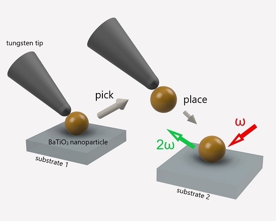
Manipulation Technique for Precise Transfer of Single Perovskite Nanoparticles


Abstract
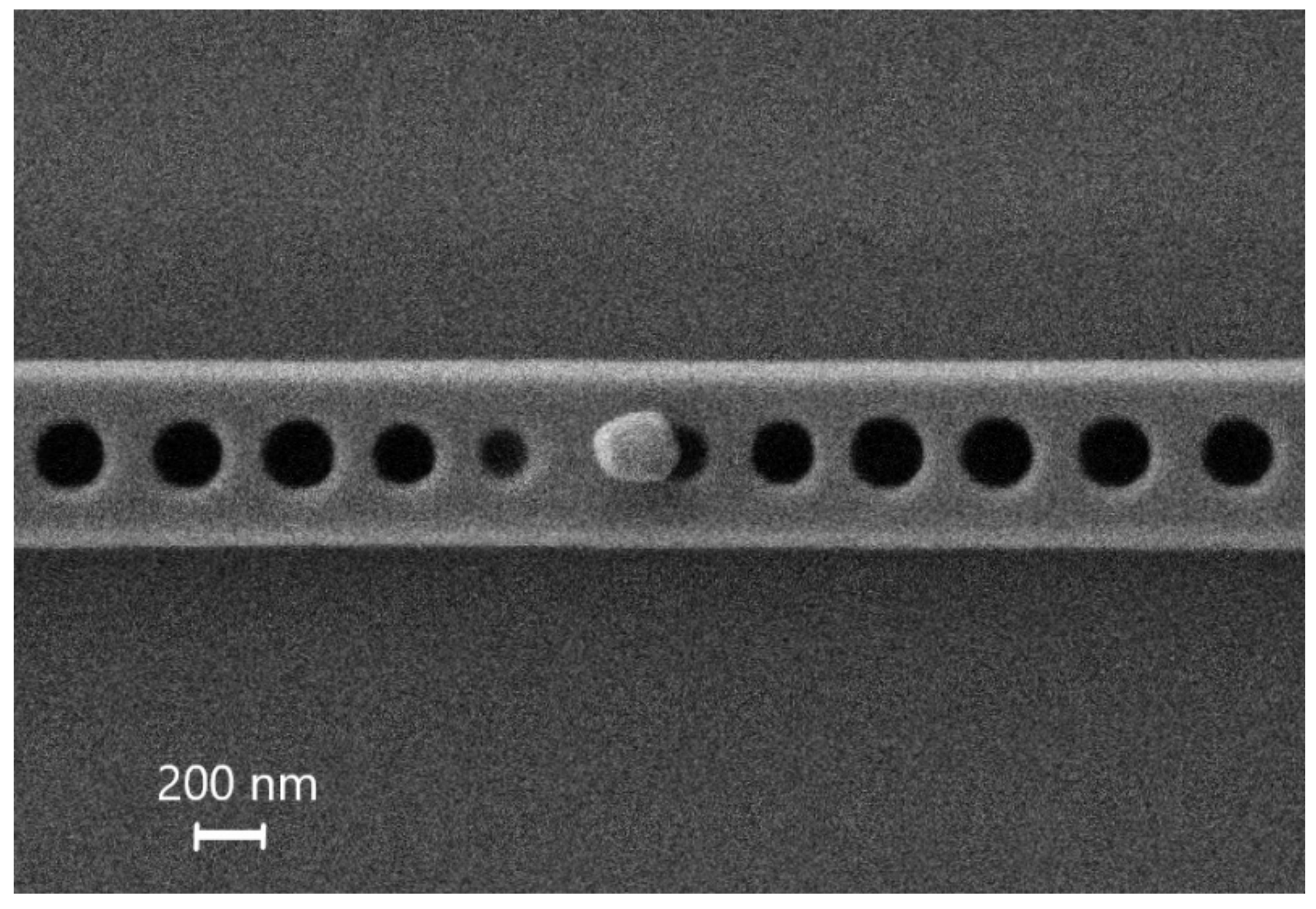
:
1. Introduction
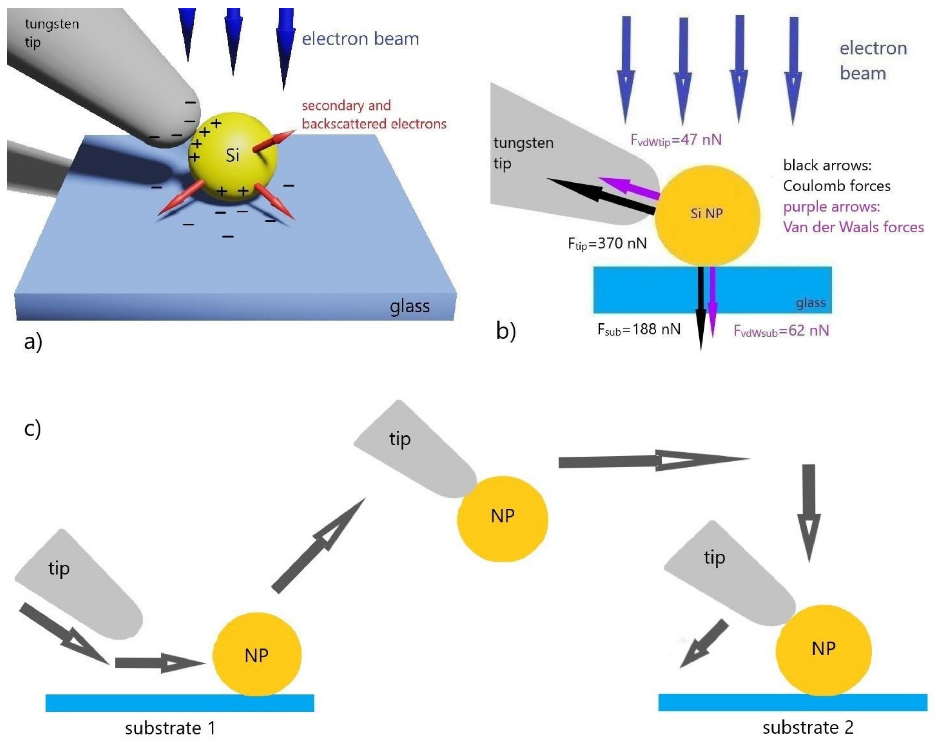
2. Materials and Methods
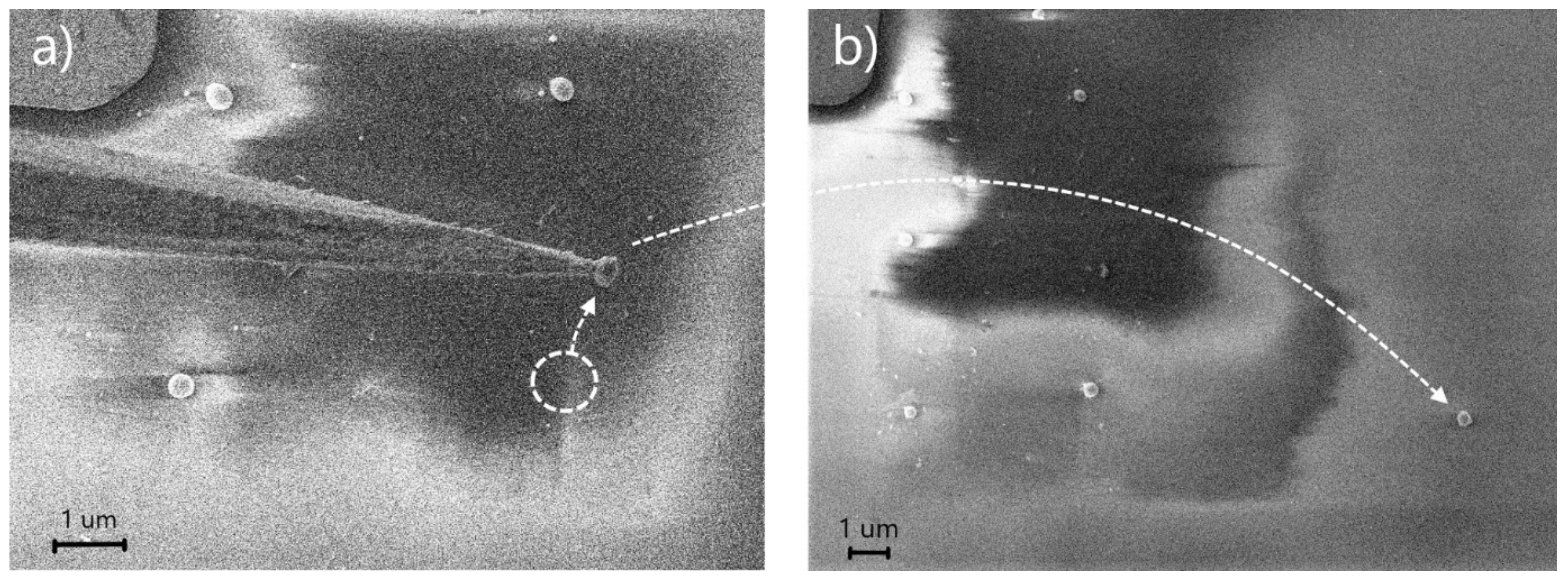
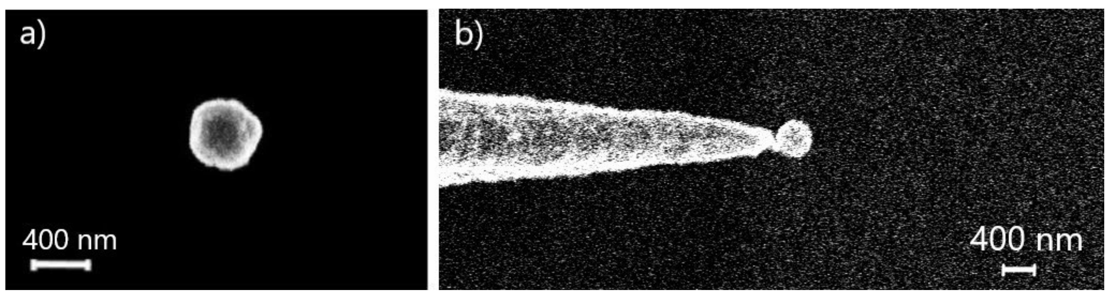
3. Results and Discussion
4. Conclusions
Author Contributions
Funding
Acknowledgments
Conflicts of Interest
References
- Jahani, S.; Jacob, Z. All-dielectric metamaterials. Nat. Nanotechnol. 2016, 11, 23–36. [Google Scholar] [CrossRef] [PubMed]
- Krasnok, A.E.; Miroshnichenko, A.E.; Belov, P.A.; Kivshar, Y.S. All-dielectric optical nanoantennas. Opt. Express 2012, 20, 20599–20604. [Google Scholar] [CrossRef] [PubMed]
- Savelev, R.S.; Makarov, S.V.; Krasnok, A.E.; Belov, P.A. From optical magnetic resonance to dielectric nanophotonics (A review). Opt. Spectrosc. 2015, 119, 551–568. [Google Scholar] [CrossRef]
- Kuznetsov, A.I.; Miroshnichenko, A.E.; Brongersma, M.L.; Kivshar, Y.S.; Luk’yanchuk, B. Optically resonant dielectric nanostructures. Science 2016, 354, aag2472. [Google Scholar] [CrossRef] [PubMed] [Green Version]
- Kruk, S.; Kivshar, Y. Functional Meta-Optics and Nanophotonics Governed by Mie Resonances. ACS Photonics 2017, 4, 2638–2649. [Google Scholar] [CrossRef] [Green Version]
- Lu, H.A.; Wills, L.A.; Wessels, B.W.; Lin, W.P.; Zhang, T.G.; Wong, G.K.; Neumayer, D.A.; Marks, T.J. Secondharmonic generation of poled BaTiO3 thin films. Appl. Phys. Lett. 1993, 62, 1314–1316. [Google Scholar] [CrossRef]
- Lin, P.T.; Wessels, B.W.; Jang, J.I.; Ketterson, J.B. Highly efficient broadband second harmonic generation using polydomain epitaxial barium titanate thin film waveguides. Appl. Phys. Lett. 2008, 92, 221103. [Google Scholar] [CrossRef]
- Kim, E.; Steinbruck, A.; Buscaglia, M.T.; Buscaglia, V.; Pertsch, T.; Grange, R. Second-harmonic generation of single BaTiO3 nanoparticles down to 22 nm diameter. ACS Nano 2013, 7, 5343–5349. [Google Scholar] [CrossRef]
- Ma, C.; Yan, J.; Wei, Y.; Liu, P.; Yang, G. Enhanced second harmonic generation in individual barium titanate nanoparticles driven by Mie resonances. J. Mater. Chem. C 2017, 5, 4810–4819. [Google Scholar] [CrossRef]
- Timpu, F.; Hendricks, N.R.; Petrov, M.; Ni, S.; Renaut, C.; Wolf, H.; Isa, L.; Kivshar, Y.; Grange, R. Enhanced second-harmonic generation from sequential capillarity-assisted particle assembly of hybrid nanodimers. Nano Lett. 2017, 17, 5381–5388. [Google Scholar] [CrossRef]
- Pu, Y.; Grange, R.; Hsieh, C.L.; Psaltis, D. Nonlinear optical properties of core-shell nanocavities for enhanced second-harmonic generation. Phys. Rev. Lett. 2010, 104, 207402. [Google Scholar] [CrossRef] [PubMed]
- Timpu, F.; Sergeyev, A.; Hendricks, N.R.; Grange, R. Second-harmonic enhancement with Mie resonances in perovskite nanoparticles. ACS Photonics 2017, 4, 76–84. [Google Scholar] [CrossRef]
- Markovich, D.L.; Ginzburg, P.; Samusev, A.K.; Belov, P.A.; Zayats, A.V. Magnetic dipole radiation tailored by substrates: Numerical investigation. Opt. Express 2014, 22, 10693–10702. [Google Scholar] [CrossRef] [Green Version]
- Xifre-Perez, E.; Shi, L.; Tuzer, U.; Fenollosa, R.; Ramiro-Manzano, F.; Quidant, R.; Meseguer, F. Mirror-image-induced magnetic modes. ACS Nano 2013, 7, 664–668. [Google Scholar] [CrossRef]
- Ashkin, A. Acceleration and trapping of particles by radiation pressure. Phys. Rev. Lett. 1970, 24, 156–159. [Google Scholar] [CrossRef] [Green Version]
- Sitti, M.; Hashimoto, H. Controlled pushing of nanoparticles: Modeling and experiments. IEEE ASME Trans. Mechatron. 2000, 5, 199–211. [Google Scholar] [CrossRef]
- Kim, S.; Shafiei, F.; Ratchford, D.; Li, X. Controlled AFM manipulation of small nanoparticles and assembly of hybrid nanostructures. Nanotechnology 2011, 22, 115301. [Google Scholar] [CrossRef] [PubMed]
- Decossas, S.; Mazen, F.; Baron, T.; Bremond, G.; Souifi, A. Atomic force microscopy nanomanipulation of silicon nanocrystals for nanodevice fabrication. Nanotechnology 2003, 14, 1272–1278. [Google Scholar] [CrossRef]
- Grobelny, J.; Tsai, D.H.; Kim, D.I.; Pradeep, N.; Cook, R.F.; Zachariah, M.R. Mechanism of nanoparticle manipulation by scanning tunnelling microscopy. Nanotechnology 2006, 17, 5519–5524. [Google Scholar] [CrossRef] [Green Version]
- Ducker, W.A.; Senden, T.J.; Pashley, R.M. Direct measurement of colloidal forces using an atomic force microscope. Nature 1991, 353, 239–241. [Google Scholar] [CrossRef]
- Mukhin, I.S.; Fadeev, I.V.; Zhukov, M.V.; Dubrovskii, V.G.; Golubok, A.O. Framed carbon nanostructures: Synthesis and applications in functional SPM tips. Ultramicroscopy 2015, 148, 151–157. [Google Scholar] [CrossRef] [PubMed]
- Mølhave, K.; Wich, T.; Kortschack, A.; Bøggild, P. Pick-and-place nanomanipulation using microfabricated grippers. Nanotechnology 2006, 17, 2434–2441. [Google Scholar] [CrossRef] [PubMed] [Green Version]
- Cagliani, A.; Wierzbicki, R.; Occhipinti, L.; Petersen, D.H.; Dyvelkov, K.N.; Sukas, Ö.S.; Herstrøm, B.G.; Booth, T.; Bøggild, P. Manipulation and in situ transmission electron microscope characterization of sub-100 nm nanostructures using a microfabricated nanogripper. J. Micromech. Microeng. 2010, 20, 035009. [Google Scholar] [CrossRef]
- Meyer, E.; Braun, H.G. Micro-and nanomanipulation inside the SEM. J. Phys. Conf. Ser. 2008, 126, 012074. [Google Scholar] [CrossRef]
- Miyazaki, H.; Sato, T. Pick and place shape forming of three-dimensional micro structures from fine particles. Proc. IEEE Int. Conf. Robot. Autom. 1996, 3, 2535–2540. [Google Scholar]
- Fukuda, T.; Arai, F.; Dong, L. Assembly of nanodevices with carbon nanotubes through nanorobotic manipulations. Proc. IEEE 2003, 91, 1803–1818. [Google Scholar] [CrossRef] [Green Version]
- Denisyuk, A.I.; Komissarenko, F.E.; Mukhin, I.S. Electrostatic pick-and-place micro/nanomanipulation under the electron beam. Microelectron. Eng. 2014, 121, 15–18. [Google Scholar] [CrossRef]
- Zheng, H.; Mirsaidov, U.M.; Wang, L.W.; Matsudaira, P. Electron beam manipulation of nanoparticles. Nano Lett. 2012, 12, 5644–5648. [Google Scholar] [CrossRef]
- Oleshko, V.P.; Howe, J.M. Electron tweezers as a tool for high-precision manipulation of nanoobjects. Adv. Imaging Electron Phys. 2013, 179, 203–262. [Google Scholar]
- Makarov, S.V.; Sinev, I.S.; Milichko, V.A.; Komissarenko, F.E.; Zuev, D.A.; Ushakova, E.V.; Mukhin, I.S.; Yu, Y.F.; Kuznetsov, A.I.; Belov, P.A.; et al. Nanoscale generation of white light for ultrabroadband nanospectroscopy. Nano Lett. 2018, 18, 535–539. [Google Scholar] [CrossRef]
- Renaut, C.; Lang, L.; Frizyuk, K.; Timofeeva, M.; Komissarenko, F.E.; Mukhin, I.S.; Smirnova, D.; Timpu, F.; Petrov, M.; Kivshar, Y.; et al. Reshaping the Second-Order Polar Response of Hybrid Metal–Dielectric Nanodimers. Nano Lett. 2019, 19, 877–884. [Google Scholar] [CrossRef] [PubMed] [Green Version]
- Lukashenko, S.Y.; Mukhin, I.S.; Komissarenko, F.E.; Gorbenko, O.M.; Sapozhnikov, I.D.; Felshtyn, M.L.; Uskov, A.V.; Golubok, A.O. Resonant Mass Detector Based on Carbon Nanowhiskers with Traps for Nanoobjects Weighing. Phys. Status Solidi A 2018, 215, 1800046. [Google Scholar] [CrossRef]
- Kryzhanovskaya, N.; Polubavkina, Y.; Moiseev, E.; Maximov, M.; Zhurikhina, V.; Scherbak, S.; Lipovskii, A.; Kulagina, M.; Zadrianov, Y.; Mukhin, I.; et al. Enhanced light outcoupling in microdisk lasers via Si spherical nanoantennas. J. Appl. Phys. 2018, 124, 163102. [Google Scholar] [CrossRef]
- Mukhin, I.; Zhukov, M.; Mozharov, A.; Bolshakov, A.; Golubok, A. Influence of condensation enhancement effect on AFM image contrast inversion in hydrophilic nanocapillaries. Appl. Surf. Sci. 2019, 471, 621–626. [Google Scholar] [CrossRef]
- Dmitriev, P.A.; Makarov, S.V.; Milichko, V.A.; Mukhin, I.S.; Gudovskikh, A.S.; Sitnikova, A.A.; Samusev, A.K.; Krasnok, A.E.; Belov, P.A. Laser fabrication of crystalline silicon nanoresonators from an amorphous film for low-loss all-dielectric nanophotonics. Nanoscale 2016, 8, 5043–5048. [Google Scholar] [CrossRef] [Green Version]
- Reimer, L. Electron scattering and diffusion. In Scanning Electron Microscopy; Springer: Berlin/Heidelberg, Germany, 1998; pp. 57–134. [Google Scholar]
- Miyazaki, H.T.; Tomizawa, Y.; Saito, S.; Sato, T.; Shinya, N. Adhesion of micrometer-sized polymer particles under a scanning electron microscope. J. Appl. Phys. 2000, 88, 3330–3340. [Google Scholar] [CrossRef]
- McMeeking, R.M.; Landis, C.M.; Jimenez, S.M. A principle of virtual work for combined electrostatic and mechanical loading of materials. Int. J. NonLin. Mech. 2007, 42, 831–838. [Google Scholar] [CrossRef]
- Fowler, R.H.; Nordheim, L. Electron emission in intense electric fields. Proc. R. Soc. Lond. A Math. Phys. 1928, 119, 173–181. [Google Scholar]
- Dyke, W.P.; Dolan, W.W. Field emission. Adv. Electron. Electron. Phys. 1956, 8, 89–185. [Google Scholar]
- Cazaux, J. Charging in scanning electron microscopy “from inside and outside”. Scanning 2004, 26, 181–203. [Google Scholar] [CrossRef]
- Hamaker, H.C. The London—Van der Waals attraction between spherical particles. Physica 1937, 4, 1058–1072. [Google Scholar] [CrossRef]
- Hu, S.; Kim, T.H.; Park, J.G.; Busnaina, A.A. Effect of different deposition mediums on the adhesion and removal of particles. J. Electrochem. Soc. 2010, 157, H662–H665. [Google Scholar] [CrossRef] [Green Version]
- Contreras-Naranjo, J.C.; Ugaz, V.M. A nanometre-scale resolution interference-based probe of interfacial phenomena between microscopic objects and surfaces. Nat. Commun. 2013, 4, 1–9. [Google Scholar] [CrossRef] [PubMed] [Green Version]
- Pin, C.; Cluzel, B.; Renaut, C.; Picard, E.; Peyrade, D.; Hadji, E.; de Fornel, F. Optofluidic near-field optical microscopy: Near-field mapping of a silicon nanocavity using trapped microbeads. ACS Photonics 2015, 2, 1410–1415. [Google Scholar] [CrossRef]

© 2020 by the authors. Licensee MDPI, Basel, Switzerland. This article is an open access article distributed under the terms and conditions of the Creative Commons Attribution (CC BY) license (http://creativecommons.org/licenses/by/4.0/).
Share and Cite
Komissarenko, F.; Zograf, G.; Makarov, S.; Petrov, M.; Mukhin, I. Manipulation Technique for Precise Transfer of Single Perovskite Nanoparticles. Nanomaterials 2020, 10, 1306. https://doi.org/10.3390/nano10071306
Komissarenko F, Zograf G, Makarov S, Petrov M, Mukhin I. Manipulation Technique for Precise Transfer of Single Perovskite Nanoparticles. Nanomaterials. 2020; 10(7):1306. https://doi.org/10.3390/nano10071306
Chicago/Turabian StyleKomissarenko, Filipp, George Zograf, Sergey Makarov, Mikhail Petrov, and Ivan Mukhin. 2020. "Manipulation Technique for Precise Transfer of Single Perovskite Nanoparticles" Nanomaterials 10, no. 7: 1306. https://doi.org/10.3390/nano10071306