Light Scattering from Rough Silver Surfaces: Modeling of Absorption Loss Measurements


Abstract
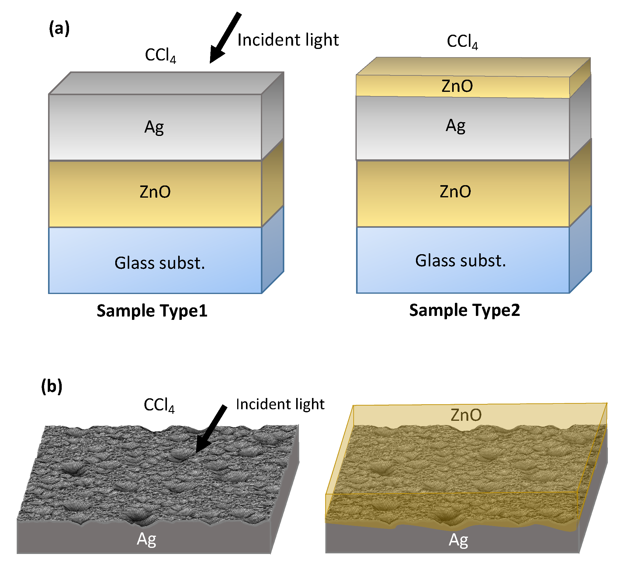
:
1. Introduction
2. Methodology
3. Results and Discussion
4. Conclusions
Author Contributions
Funding
Data Availability Statement
Acknowledgments
Conflicts of Interest
References
- Chong, T.K.; Wilson, J.; Mokkapati, S.; Catchpole, K.R. Optimal wavelength scale diffraction gratings for light trapping in solar cells. J. Opt. 2012, 14, 024012. [Google Scholar] [CrossRef] [Green Version]
- Joannopoulos, J.D.; Johnson, S.G.; Winn, J.N.; Meade, R.D. Photonic Crystals: Molding the Flow of Light, 2nd ed.; Princeton University Press: Princeton, NJ, USA, 2008. [Google Scholar]
- David, C. TiO2 Self-Assembled, Thin-Walled Nanotube Arrays for Photonic Applications. Materials 2019, 12, 1332. [Google Scholar] [CrossRef] [Green Version]
- Jakšić, Z.; Vuković, S.; Matovic, J.; Tanasković, D. Negative Refractive Index Metasurfaces for Enhanced Biosensing. Materials 2010, 4, 1. [Google Scholar] [CrossRef] [Green Version]
- Yan, J.; Liu, X.; Ma, C.; Huang, Y.; Yang, G. All-dielectric materials and related nanophotonic applications. Mater. Sci. Eng. R Rep. 2020, 141, 100563. [Google Scholar] [CrossRef]
- Genet, C.; Ebbesen, T.W. Light in tiny holes. Nature 2007, 445, 39–46. [Google Scholar] [CrossRef]
- Jonsson, M.P.; Dahlin, A.B.; Jönsson, P.; Höök, F. Nanoplasmonic biosensing with focus on short-range ordered nanoholes in thin metal films. Biointerphases 2008, 3, FD30–FD40. [Google Scholar] [CrossRef] [PubMed] [Green Version]
- García de Abajo, F.J. Optical excitations in electron microscopy. Rev. Mod. Phys. 2010, 82, 209–275. [Google Scholar] [CrossRef]
- David, C.; Christensen, J.; Mortensen, N.A. Spatial dispersion in two-dimensional plasmonic crystals: Large blueshifts promoted by diffraction anomalies. Phys. Rev. B 2016, 94, 165410. [Google Scholar] [CrossRef] [Green Version]
- David, C.; Christensen, J. Extraordinary optical transmission through nonlocal holey metal films. Appl. Phys. Lett. 2017, 110, 261110. [Google Scholar] [CrossRef] [Green Version]
- Morarescu, R.; Englert, L.; Kolaric, B.; Damman, P.; Vallee, R.A.L.; Baumert, T.; Hubenthal, F.; Trager, F. Tuning nanopatterns on fused silica substrates: A theoretical and experimental approach. J. Mater. Chem. 2011, 21, 4076–4081. [Google Scholar] [CrossRef]
- David, C.; Kühler, P.; Javier García de Abajo, F.; Siegel, J. Near-field nanoimprinting using colloidal monolayers. Opt. Express 2014, 22, 8226–8233. [Google Scholar] [CrossRef] [PubMed]
- Kumar, P.S.; Pastoriza-Santos, I.; Rodríguez-González, B.; de Abajo, F.J.G.; Liz-Marzán, L.M. High-yield synthesis and optical response of gold nanostars. Nanotechnology 2008, 19, 015606. [Google Scholar] [CrossRef]
- Sarkar, S.; Gupta, V.; Kumar, M.; Schubert, J.; Probst, P.T.; Joseph, J.; König, T.A. Hybridized Guided-Mode Resonances via Colloidal Plasmonic Self-Assembled Grating. ACS Appl. Mater. Interfaces 2019, 11, 13752–13760. [Google Scholar] [CrossRef] [Green Version]
- Li, L.; Guo, W.; Wang, Z.B.; Liu, Z.; Whitehead, D.; Luk’yanchuk, B. Large-area laser nano-texturing with user-defined patterns. J. Micromech. Microeng. 2009, 19, 054002. [Google Scholar] [CrossRef]
- Roy, P.; Berger, S.; Schmuki, P. TiO2 Nanotubes: Synthesis and Applications. Angew. Chem. Int. Ed. 2011, 50, 2904–2939. [Google Scholar] [CrossRef] [PubMed]
- Öner, I.H.; Querebillo, C.J.; David, C.; Gernert, U.; Walter, C.; Driess, M.; Leimkühler, S.; Ly, K.H.; Weidinger, I.M. High Electromagnetic Field Enhancement of TiO2 Nanotube Electrodes. Angew. Chem. Int. Ed. 2018, 57, 7225–7229. [Google Scholar] [CrossRef] [PubMed]
- Akimov, A.V.; Neukirch, A.J.; Prezhdo, O.V. Theoretical Insights into Photoinduced Charge Transfer and Catalysis at Oxide Interfaces. Chem. Rev. 2013, 113, 4496–4565. [Google Scholar] [CrossRef] [PubMed]
- Ma, X.C.; Dai, Y.; Yu, L.; Huang, B.B. Energy transfer in plasmonic photocatalytic composites. Light Sci. Appl. 2016, 5, e16017. [Google Scholar] [CrossRef] [PubMed] [Green Version]
- David, C. Two-fluid, hydrodynamic model for spherical electrolyte systems. Sci. Rep. 2018, 8, 7544. [Google Scholar] [CrossRef]
- Wang, E.; White, T.P.; Catchpole, K.R. Resonant enhancement of dielectric and metal nanoparticle arrays for light trapping in solar cells. Opt. Express 2012, 20, 13226–13237. [Google Scholar] [CrossRef]
- Villanueva-Cab, J.; Montaño-Priede, J.L.; Pal, U. Effects of Plasmonic Nanoparticle Incorporation on Electrodynamics and Photovoltaic Performance of Dye Sensitized Solar Cells. J. Phys. Chem. C 2016, 120, 10129–10136. [Google Scholar] [CrossRef]
- Feng, J.J.; Gernert, U.; Sezer, M.; Kuhlmann, U.; Murgida, D.H.; David, C.; Richter, M.; Knorr, A.; Hildebrandt, P.; Weidinger, I.M. Novel Ag-Au Hybrid Device for Electrochemical SE(R)R Spectroscopy in a Wide Potential and Spectral Range. Nano Lett. 2009, 9, 298–303. [Google Scholar] [CrossRef]
- David, C.; Richter, M.; Knorr, A.; Weidinger, I.M.; Hildebrandt, P. Image dipoles approach to the local field enhancement in nanostructured Ag-Au hybrid devices. J. Chem. Phys. 2010, 132, 024712. [Google Scholar] [CrossRef] [PubMed]
- David, C.; Connolly, J.P.; Chaverri Ramos, C.; García de Abajo, F.J.; Sánchez Plaza, G. Theory of random nanoparticle layers in photovoltaic devices applied to self-aggregated metal samples. Sol. Energy Mater. Sol. Cells 2013, 109, 294–299. [Google Scholar] [CrossRef] [Green Version]
- David, C. Multi-type particle layer improved light trapping for photovoltaic applications. Appl. Opt. 2016, 55, 7980–7986. [Google Scholar] [CrossRef] [PubMed] [Green Version]
- Hamed, T.A.; Adamovic, N.; Aeberhard, U.; Alonso-Alvarez, D.; Amin-Akhlaghi, Z.; der Maur, M.A.; Beattie, N.; Bednar, N.; Berland, K.; Califano, M.; et al. Multiscale in modelling and validation for solar photovoltaics. EPJ Photovolt. 2018, 9, 10. [Google Scholar] [CrossRef]
- Springer, J.; Poruba, A.; Müllerova, L.; Vanecek, M.; Kluth, O.; Rech, B. Absorption loss at nanorough silver back reflector of thin-film silicon solar cells. J. Appl. Phys. 2004, 95, 1427–1429. [Google Scholar] [CrossRef] [Green Version]
- Jäger, K.; Zeman, M. A scattering model for surface-textured thin films. Appl. Phys. Lett. 2009, 95, 171108. [Google Scholar] [CrossRef] [Green Version]
- Battaglia, C.; Söderström, K.; Escarré, J.; Haug, F.J.; Dominé, D.; Cuony, P.; Boccard, M.; Bugnon, G.; Denizot, C.; Despeisse, M.; et al. Efficient light management scheme for thin film silicon solar cells via transparent random nanostructures fabricated by nanoimprinting. Appl. Phys. Lett. 2010, 96, 213504. [Google Scholar] [CrossRef] [Green Version]
- Dominé, D.; Haug, F.J.; Battaglia, C.; Ballif, C. Modeling of light scattering from micro- and nanotextured surfaces. J. Appl. Phys. 2010, 107, 044504. [Google Scholar] [CrossRef]
- Jäger, K.; Fischer, M.; van Swaaij, R.A.C.M.M.; Zeman, M. A scattering model for nano-textured interfaces and its application in opto-electrical simulations of thin-film silicon solar cells. J. Appl. Phys. 2012, 111, 083108. [Google Scholar] [CrossRef]
- Whittaker, D.M.; Culshaw, I.S. Scattering-matrix treatment of patterned multilayer photonic structures. Phys. Rev. B 1999, 60, 2610–2618. [Google Scholar] [CrossRef] [Green Version]
- Liu, V.; Fan, S. S4: A free electromagnetic solver for layered periodic structures. Comput. Phys. Commun. 2012, 183, 2233–2244. [Google Scholar] [CrossRef]
- Sehmi, H.S.; Langbein, W.; Muljarov, E.A. Optimizing the Drude-Lorentz model for material permittivity: Method, program, and examples for gold, silver, and copper. Phys. Rev. B 2017, 95. [Google Scholar] [CrossRef] [Green Version]
- Available online: http://gwyddion.net/ (accessed on 18 April 2020).
- David, C.; García de Abajo, F.J. Spatial Nonlocality in the Optical Response of Metal Nanoparticles. J. Phys. Chem. C 2011, 115, 19470–19475. [Google Scholar] [CrossRef]
- David, C.; Mortensen, N.A.; Christensen, J. Perfect imaging, epsilon-near zero phenomena and waveguiding in the scope of nonlocal effects. Sci. Rep. 2013, 3, 2526. [Google Scholar] [CrossRef] [Green Version]
- David, C.; García de Abajo, F.J. Surface Plasmon Dependence on the Electron Density Profile at Metal Surfaces. ACS Nano 2014, 8, 9558–9566. [Google Scholar] [CrossRef]
- Raza, S.; Wubs, M.; Bozhevolnyi, S.I.; Mortensen, N.A. Nonlocal study of ultimate plasmon hybridization. Opt. Lett. 2015, 40, 839–842. [Google Scholar] [CrossRef] [Green Version]
- Kluczyk, K.; Jacak, L.; Jacak, W.; David, C. Microscopic Electron Dynamics in Metal Nanoparticles for Photovoltaic Systems. Materials 2018, 11, 1077. [Google Scholar] [CrossRef] [Green Version]
- Kluczyk-Korch, K.; Jacak, L.; Jacak, W.A.; David, C. Mode Splitting Induced by Mesoscopic Electron Dynamics in Strongly Coupled Metal Nanoparticles on Dielectric Substrates. Nanomaterials 2019, 9, 1206. [Google Scholar] [CrossRef] [Green Version]


| Type 1 rms (nm) | Type 2 rms (nm) | Ag Thickness (nm) |
|---|---|---|
| 8.86 | 8.86 | 65 |
| 30.48 | 30.48 | 85 |
| 76.34 | 73.51 | 105 |
| 107.69 | 110.48 | 195 |
| 134.17 | 130.19 | 255 |
| 151.97 | 155.81 | 315 |
| 0 (flat) | 0 (flat) | 315 |
| This Work | Gwyddion | Ref. [28] |
|---|---|---|
| 9.30 | 9.34 | 14 |
| 30.48 | 30.44 | 37 |
| 76.34 | 76.21 | 74 |
| 107.69 | 107.50 | 106 |
| 134.17 | 133.90 | 131 |
| 151.97 | 151.60 | 146 |
Publisher’s Note: MDPI stays neutral with regard to jurisdictional claims in published maps and institutional affiliations. |
© 2021 by the authors. Licensee MDPI, Basel, Switzerland. This article is an open access article distributed under the terms and conditions of the Creative Commons Attribution (CC BY) license (http://creativecommons.org/licenses/by/4.0/).
Share and Cite
Dehghani, M.; David, C. Light Scattering from Rough Silver Surfaces: Modeling of Absorption Loss Measurements. Nanomaterials 2021, 11, 113. https://doi.org/10.3390/nano11010113
Dehghani M, David C. Light Scattering from Rough Silver Surfaces: Modeling of Absorption Loss Measurements. Nanomaterials. 2021; 11(1):113. https://doi.org/10.3390/nano11010113
Chicago/Turabian StyleDehghani, Matin, and Christin David. 2021. "Light Scattering from Rough Silver Surfaces: Modeling of Absorption Loss Measurements" Nanomaterials 11, no. 1: 113. https://doi.org/10.3390/nano11010113
APA StyleDehghani, M., & David, C. (2021). Light Scattering from Rough Silver Surfaces: Modeling of Absorption Loss Measurements. Nanomaterials, 11(1), 113. https://doi.org/10.3390/nano11010113