Article

Enhanced Optoelectronic Performance of Yellow Light-Emitting Diodes Grown on InGaN/GaN Pre-Well Structure

1
Center for Photonics and Semiconductors, School of Power and Mechanical Engineering, Wuhan University, Wuhan 430072, China
2
The Institute of Technological Sciences, Wuhan University, Wuhan 430072, China
*
Author to whom correspondence should be addressed.
Nanomaterials 2021, 11(12), 3231; https://doi.org/10.3390/nano11123231
Submission received: 6 November 2021 / Revised: 21 November 2021 / Accepted: 26 November 2021 / Published: 28 November 2021

Abstract

:
InGaN-based long-wavelength light-emitting diodes (LEDs) are indispensable components for the next-generation solid-state lighting industry. In this work, we introduce additional InGaN/GaN pre-wells in LED structure and investigate the influence on optoelectronic properties of yellow (~575 nm) LEDs. It is found that yellow LED with pre-wells exhibits a smaller blue shift, and a 2.2-fold increase in light output power and stronger photoluminescence (PL) intensity compared to yellow LED without pre-wells. The underlying mechanism is revealed by using Raman spectra, temperature-dependent PL, and X-ray diffraction. Benefiting from the pre-well structure, in-plane compressive stress is reduced, which effectively suppresses the quantum confined stark effect. Furthermore, the increased quantum efficiency is also related to deeper localized states with reduced non-radiative centers forming in multiple quantum wells grown on pre-wells. Our work demonstrates a comprehensive understanding of a pre-well structure for obtaining efficient LEDs towards long wavelengths.

1. Introduction

III-nitride emitters have attracted a lot of attention due to their advantages of energy savings, high brightness, and long lifetime. With the wide and tunable band gap, InGaN-based light emitting diodes (LEDs) find widespread applications in the solid-state lighting and full-color display [1,2,3,4,5,6,7]. In recent years, the increasing need of flexible lighting devices motivates the manufacturing techniques development for deformable micro-LEDs [8] and the progress of flexible micro-LEDs applications in the optogenetic biomedical field [9]. Though blue LEDs achieving a high external quantum efficiency [10], the emission efficiency is still limited in the long-wavelength region, which is commonly known as “green-yellow gap” phenomenon [2]. One of the main reasons arises from the strong piezoelectric field along the (0001) direction induced by the large lattice mismatch between sapphire substrate and epilayers. This built-in piezoelectric field gives rise to quantum-confined stark effect (QCSE) [11], which separates electron-hole wavefunctions and further degrades the radiative recombination efficiency. When the In content increases, QCSE becomes more severe, hindering the pursuit for efficient LEDs with long wavelengths.
Numerous efforts have been dedicated to improving the InGaN-based LED performance in the long-wavelength region, such as introducing semipolar/nonpolar substrate [12], inserting strain engineering layers [13,14], and adopting bandgap engineering quantum wells [15,16]. Among them, the strain engineering strategy, which utilizes low In content layers prior to the growth of active region, is an effective and low-cost method, also known as the “pre-layer structure”. Huang et al. found that a green LED structure with pre-strained growth showed enhanced efficiency and reduced spectral shifts, which could be attributed to decreased defect density and the reduced QCSE [17]. Niu et al. reported that insertion of an InGaN layer increased photoluminescence (PL) intensity more than twice as much, and improved crystal quality [18]. The inclusion of InGaN/GaN superlattice pre-layers could facilitate more In incorporation and extend emission wavelength, as Hu et al. demonstrated [19]. The pre-layer structure could act as the buffer layer to relax in-plane strain in multiple quantum wells (MQWs). Until now, while various pre-layers have been extensively discussed in blue and green region [14,17,18,19,20,21], their epitaxial structures differ much from corresponding MQWs. Besides, the influence of pre-layer structure on yellow LEDs performance remains insufficient [13,22], especially in terms of some related physic issues, including the effect of carrier localization.
In this work, we adopt an InGaN/GaN pre-well structure between superlattices and active region, and study its influence on optoelectronic characteristics of yellow (~575 nm) LEDs. At the same injection current, LED with pre-wells achieves a smaller blue shift and a higher light output power (LOP) than those of LED without pre-wells. Raman spectra show that relaxation of compressive strain is achieved inside MQWs grown on InGaN/GaN pre-wells, which alleviates the negative influence of QCSE. Additionally, through time-dependent photoluminescence (TDPL) and X-ray diffraction (XRD) analysis, localized states are found to be more pronounced in MQWs grown on pre-well structure, owing to the decreased dislocation density. Due to these advantages, yellow LED with pre-wells exhibits improved optical and electrical properties, enabling the development for efficient III-nitride emitters.

2. Experiments

The LED samples were grown on the patterned sapphire substrate (PSS) via metal organic chemical vapor deposition (MOCVD). The schematic diagram of two types of yellow LED structure is presented in Figure 1a. The reference LED (LED I) started from a 3.0-µm-thick undoped GaN layer. Subsequently, a 2.0-µm-thick Si-doped n-GaN layer was deposited, followed by three pairs of In0.01Ga0.99N (7 nm)/GaN (50 nm) superlattices (SLs). The active region consists of nine pairs of In0.1Ga0.9N (0.6 nm)/In0.35Ga0.65N (1.3 nm)/In0.1Ga0.9N (0.6 nm)/GaN (13 nm). Then, a 25-nm-thick low-temperature p-GaN layer was capped on MQWs. Then, a 20-nm-thick AlGaN electron-blocking layer and a 50-nm-thick Mg-doped p-GaN layer were grown, ending with a 5-nm-thick heavily Mg-doped p+-GaN. For the optimized LED (LED II), prior to the growth of MQWs, five pairs of In0.05Ga0.95N (2 nm)/GaN (10 nm) SLs, named as pre-wells, were deposited on three pairs of SLs. Notably, different from aforementioned pre-layer structures, the thicknesses of pre-wells in this work was intentionally designed to be similar to MQWs, with an aim to further reduce the lattice mismatch between underlayers and MQWs. Figure 1b shows the temperature profile during the growth of two LED structures, in which the only difference is the additional growth of pre-wells. A detailed description of fabrication of LED chips has been provided in our previous work [23]. The LED chips were fabricated with areas of 239 μm × 356 μm.
To characterize the epitaxial structure of LED samples, we carried out the cross-sectional transmission electron microscopy (TEM), atom probe tomography (APT), Raman spectroscopy, and X-ray diffraction (XRD) measurements. The light output power–current–voltage (L-I-V) characteristics of the yellow LEDs were measured by an integrating sphere together with a semiconductor parameter analyzer at room temperature. TDPL measurements were performed using a 325-nm He–Cd laser with an excitation power of 5 mW.

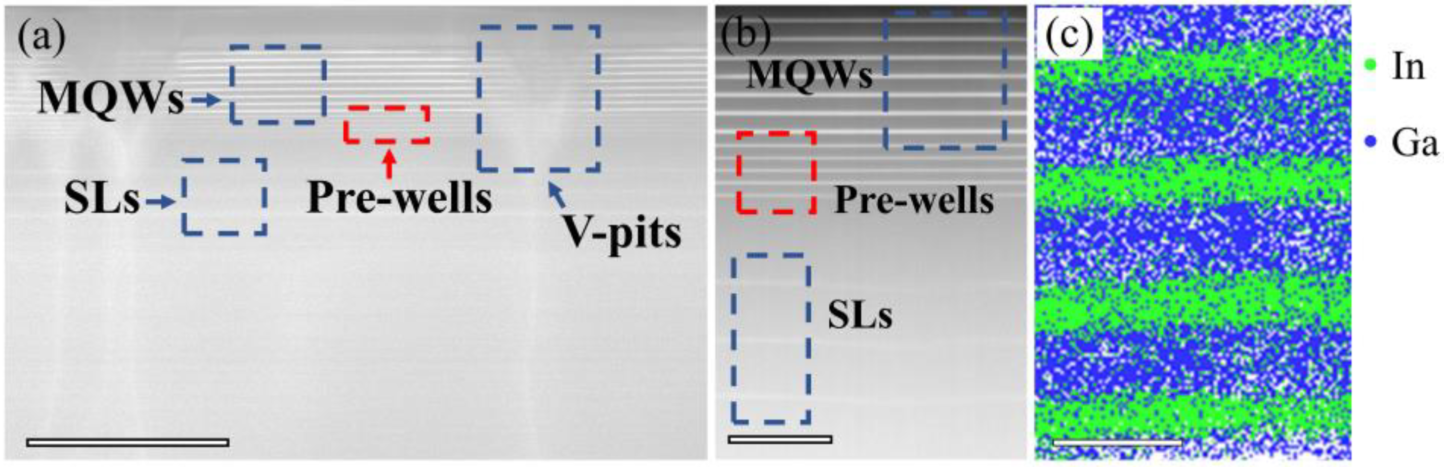
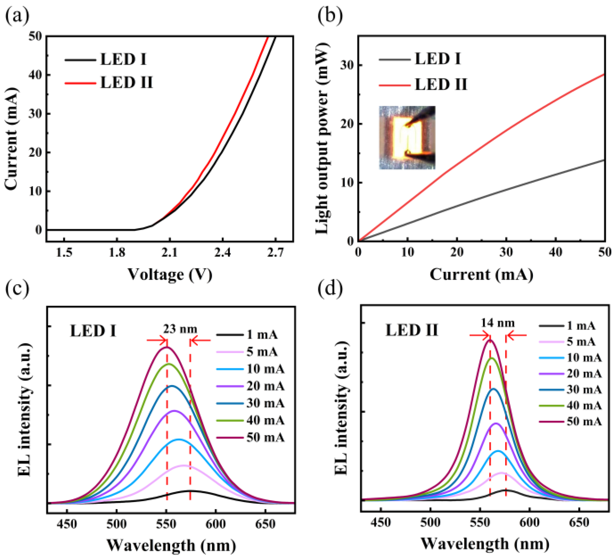
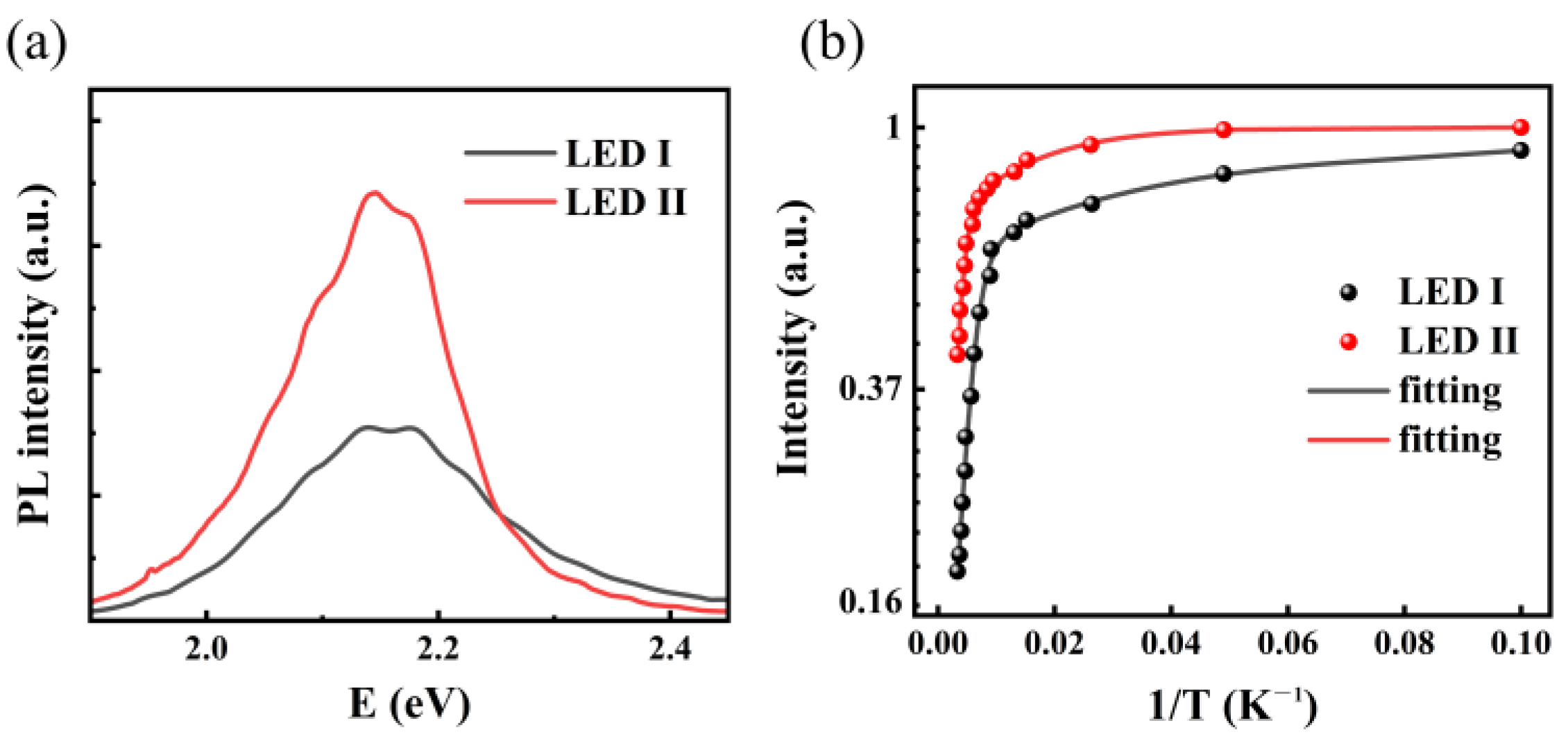
3. Results and Discussion

Figure 2a,b show the cross-sectional bright-field TEM images of epilayer structure with pre-wells. Each layer in LED II exhibits uniform thickness and clear interface, albeit the difference in brightness contrasts among SLs, pre-wells, and MQWs, as seen in Figure 2a,b. Besides, from Figure 2a, we observe that V-shaped pits form in SLs and extend to MQWs. Our previous work found that optimizing the density and size of V-pits could contribute to the increased emission efficiency by suppressing non-radiative recombination [23]. Figure 2c shows the reconstructed atom map of MQWs of LED II via APT measurement, showing the distribution of In and Ga elements.
Figure 3a,b show the current–voltage (I-V) and light output power–current (L-I) characteristics of the yellow LEDs, respectively. In Figure 3a, the forward voltages for LED I and LED II are 2.39 V and 2.36 V at 20 mA, respectively. This indicates that the pre-well structure has a negligible impact on the electrical properties. Note that LED II has an enhanced LOP in compared with LED I. At 20 mA, the LOP for LED I is 5.9 mW, while that for LED II is 13 mW. Room-temperature electroluminescence (EL) measurements were performed and shown in Figure 3c,d. As the injection current increases, the peak wavelengths for two samples are observed in the blue shift, which arises from the charge screening of polarization field and band-filling effect [24]. It could be observed that LED II shows a much smaller blue shift (~14 nm) than LED I (~23 nm) when the injection current increases from 1 mA to 50 mA. For most InGaN MQWs grown on c-plane sapphire, they undergo QCSE which causes strong band tilting and wavelength shifting. As the carriers are injected, the built-in electric field are screened, leading to a decreased wavelength shift. Thus, we believe that, with the inclusion of a pre-well structure, a negative impact of QCSE is alleviated, and the LED with pre-wells achieves a smaller blue shift. Besides, from the EL spectra, there is no additional peak induced by the emission in In0.05Ga0.95N/GaN pre-wells, implying that a recombination in MQWs dominates the recombination process in our designed structure.
In order to reveal the underlying mechanism of improved performance, we carried out the confocal micro-Raman measurement, as shown in Figure 4. As the E2 (H) mode is sensitive to the strain [25], it is widely utilized to assess the residual stress in epitaxial structure. However, considering the pre-well structure located between the thick GaN layer and MQWs, the InGaN E2 (H) mode is suitable for evaluating the residual stress in MQWs. In the Raman spectra, there are two peaks positioned at ~569 cm−1 and ~560 cm−1, which originate from the GaN E2 (H) and InGaN E2 (H) mode, respectively [26]. In particular, the InGaN E2 (H) mode decreases from 562.7 cm−1 (LED I) to 559.9 cm−1 (LED II). It indicates that the adoption of pre-wells contributes to stress relaxation [26], which could be attributed to the similar structure between pre-wells and MQWs. It is well known that QCSE separates the electron and the hole wavefunctions towards the opposite direction and reduces the electron-hole wavefunction overlap, thereby deteriorating the radiative recombination rate [15]. By adopting pre-well, the negative impact of stress-induced QCSE is suppressed and, more so, the quantum efficiency is enhanced. As a result, LED II achieves improved LOP as well as the smaller blue shift (Figure 3).
The room-temperature PL spectra are shown in Figure 5a. LED II possesses a higher PL peak intensity than that of LED I, which means enhanced radiative recombination by introducing pre-well structure. Figure 5b shows the TDPL spectra. The PL intensity of LEDs dramatically decreases with increasing temperature. Such thermal quenching of PL intensity results from the pho-non-assisted non-radiative recombination and the integrated PL intensity versus temperature can be fitted by using the Arrhenius formula [27]:
I ( T ) = I 0 / [ 1 + i C i exp ( E Ai / k B T ) ]
where I (T) represents the normalized integrated PL intensity, Ci represents the constants, and EAi represents the activation energies correlated with nonradiative recombination process. In particular, EA1 and EA2 can be attributed to (1) localized exciton binding energy, and (2) the potential barrier between the localized potential minima and nonradiative centers located within MQWs, respectively [28]. Through the curve fitting, the yielding activation energies are 3.04 meV (E1) and 53.68 meV (E2) for LED I, while those for LED II are 6.89 meV (E1) and 85.64 meV (E2), respectively. Since the obtained activation energies are much lower than the band offsets between wells and barriers, thermal quenching of PL intensity results from the delocalization of excitons [29]. The activation energies often reflect the localization energy of localized states [30], in which carriers could be trapped and have less possibility to meet other non-radiative recombination centers. Accordingly, we suppose pronounced localized states existing in the pre-well structure, which provides strong confinement for carriers and preventing them from being captured by non-radiative recombination centers.
To elucidate our finding, XRD measurements were performed to assess the non-radiative centers density existing in the two samples. It is acknowledged that the full width at half maximum (FWHM) of XRD ω-rocking curves for different planes could reflect the specific threading dislocation, including screw dislocation and the edge dislocation in the epitaxial structure. Figure 6a,b shows the XRD ω-rocking curves for (002) and (102) planes of two samples, respectively. We find that, in LED II, FWHMs of ω-rocking curves for both (002) and (102) planes are 147.50 and 243.18 arcsec, respectively, while they are 176.77 and 363.93 arcsec, respectively, in LED I. Threading dislocation density (TDD) in two samples is roughly estimated through the formula [31]:
N = β 2 4 × | b | 2
where N represents the TDD, β represents the FWHM of the rocking curve, and b represents the Burgers vector of the corresponding dislocations. The total TDDs in LED I and LED II are estimated to be 8.34 × 10⁸ and 3.89 × 108 cm−2, respectively. This implies that threading dislocations, acting as non-radiative centers, are reduced by adopting pre-wells. Carrier localization has been reported to occur in the direct vicinity of the dislocation through the formation of In–N chains and atomic condensates [32]. In particular, the clustered dislocations tend to screen the effects of carrier localization, and thus the LED I with more TDD, displays the weakened carrier localization compared to LED II, leading to the inferior quantum efficiency.

4. Conclusions

In summary, we make comprehensive analysis of InGaN-based yellow (~575 nm) LED performance by adopting the InGaN/GaN pre-well structure. LED with pre-wells exhibits better optoelectronic properties, especially an increase in LOP of 13 mW, which is 2.2 times higher than that for LED without pre-wells at 20 mA. Experiment results reveal that this structure plays a vital role for stress relaxation. The performance enhancement is attributed to alleviated detrimental influence of QCSE and strengthened carrier localization in MQWs grown on pre-wells. Our work gains insight into the influence of pre-well structure on InGaN-based long-wavelength LEDs, by presenting their advantages for the future solid-state lighting.

Author Contributions

Methodology, X.Z. and S.Z.; formal analysis, X.Z., Z.W. and S.Z.; investigation, X.Z., Z.W. and S.Z.; data curation, Z.W., L.G. and G.T.; resources, S.Z.; writing—original draft preparation, X.Z. and S.Z.; writing—review and editing, X.Z., Z.W., L.G., G.T. and S.Z; supervision, S.Z.; project administration, S.Z.; funding acquisition, S.Z. All authors have read and agreed to the published version of the manuscript.

Funding

This research was funded by the National Natural Science Foundation of China (Grant Nos. 52075394, 51675386 and 51775387) and the National Youth Talent Support Program.

Data Availability Statement

Data are contained within the article.

Conflicts of Interest

The authors declare no conflict of interest.

References

  1. Pimputkar, S.; Speck, J.S.; DenBaars, S.P.; Nakamura, S. Prospects for LED lighting. Nat. Photon. 2009, 3, 180–182. [Google Scholar] [CrossRef]
  2. Crawford, M.H. LEDs for solid-state lighting: Performance challenges and recent advances. IEEE J. Sel. Top. Quantum Electron. 2009, 15, 1028–1040. [Google Scholar] [CrossRef]
  3. Hu, H.; Tang, B.; Wan, H.; Sun, H.; Zhou, S.; Dai, J.; Chen, C.; Liu, S.; Guo, L.J. Boosted ultraviolet electroluminescence of InGaN/AlGaN quantum structures grown on high-index contrast patterned sapphire with silica array. Nano Energy 2020, 69, 104427. [Google Scholar] [CrossRef]
  4. Zhou, S.; Liu, X.; Yan, H.; Chen, Z.; Liu, Y.; Liu, S. Highly efficient GaN-based high-power flip-chip light-emitting diodes. Opt. Express 2019, 27, A669–A692. [Google Scholar] [CrossRef] [PubMed]
  5. Mun, S.H.; Kang, C.M.; Min, J.H.; Choi, S.Y.; Jeong, W.L.; Kim, G.G.; Lee, J.S.; Kim, K.P.; Ko, H.C.; Lee, D.S. Highly Efficient Full-Color Inorganic LEDs on a Single Wafer by Using Multiple Adhesive Bonding. Adv. Mater. Interfaces 2021, 8, 1–7. [Google Scholar] [CrossRef]
  6. Tao, G.; Zhao, X.; Zhou, S. Stacked GaN/AlN last quantum barrier for high-efficiency InGaN-based green light-emitting diodes. Opt. Lett. 2021, 46, 4593–4596. [Google Scholar] [CrossRef] [PubMed]
  7. Tang, B.; Gong, L.; Hu, H.; Sun, H.; Zhou, S. Toward efficient long-wavelength III-nitride emitters using a hybrid nucleation layer. Opt. Express 2021, 29, 27404. [Google Scholar] [CrossRef]
  8. Jeong, J.; Wang, Q.; Cha, J.; Jin, D.K.; Shin, D.H.; Kwon, S.; Kang, B.K.; Jang, J.H.; Yang, W.S.; Choi, Y.S.; et al. Remote heteroepitaxy of GaN microrod heterostructures for deformable light-emitting diodes and wafer recycle. Sci. Adv. 2020, 6, z5180. [Google Scholar] [CrossRef] [PubMed]
  9. Lee, H.E.; Park, J.H.; Jang, D.; Shin, J.H.; Im, T.H.; Lee, J.H.; Hong, S.K.; Wang, H.S.; Kwak, M.S.; Peddigari, M.; et al. Optogenetic brain neuromodulation by stray magnetic field via flash-enhanced magneto-mechano-triboelectric nanogenerator. Nano Energy 2020, 75, 104951. [Google Scholar] [CrossRef]
  10. Narukawa, Y.; Ichikawa, M.; Sanga, D.; Sano, M.; Mukai, T. White light emitting diodes with super-high luminous efficacy. J. Phys. D Appl. Phys. 2010, 43, 354002. [Google Scholar] [CrossRef]
  11. Takeuchi, T.; Sota, S.; Katsuragawa, M.; Komori, M.; Takeuchi, H.; Amano, H.; Akasaki, I. Quantum-confined Stark effect due to piezoelectric fields in GaInN strained quantum wells. Jpn. J. Appl. Phys. 1997, 36, L382–L385. [Google Scholar] [CrossRef]
  12. Masui, H.; Nakamura, S.; DenBaars, S.P.; Mishra, U.K. Nonpolar and semipolar III-nitride light-emitting diodes: Achievements and challenges. IEEE Trans. Electron Devices 2010, 57, 88–100. [Google Scholar] [CrossRef]
  13. Jiang, F.; Zhang, J.; Xu, L.; Ding, J.; Wang, G.; Wu, X.; Wang, X.; Mo, C.; Quan, Z.; Guo, X.; et al. Efficient InGaN-based yellow-light-emitting diodes. Photon. Res. 2019, 7, 144–148. [Google Scholar] [CrossRef]
  14. Leem, S.J.; Shin, Y.C.; Kim, K.C.; Kim, E.H.; Sung, Y.M.; Moon, Y.; Hwang, S.M.; Kim, T.G. The effect of the low-mole InGaN structure and InGaN/GaN strained layer superlattices on optical performance of multiple quantum well active layers. J. Cryst. Growth 2008, 311, 103–106. [Google Scholar] [CrossRef]
  15. Zhao, H.; Liu, G.; Zhang, J.; Poplawsky, J.D.; Dierolf, V.; Tansu, N. Approaches for high internal quantum efficiency green InGaN light-emitting diodes with large overlap quantum wells. Opt. Express 2011, 19, A991–A1007. [Google Scholar] [CrossRef] [PubMed] [Green Version]
  16. Zhao, X.; Tang, B.; Gong, L.; Bai, J.; Ping, J.; Zhou, S. Rational construction of staggered InGaN quantum wells for efficient yellow light-emitting diodes. Appl. Phys. Lett. 2021, 118, 182102. [Google Scholar] [CrossRef]
  17. Huang, C.F.; Liu, T.C.; Lu, Y.C.; Shiao, W.Y.; Chen, Y.S.; Wang, J.K.; Lu, C.F.; Yang, C.C. Enhanced efficiency and reduced spectral shift of green light-emitting-diode epitaxial structure with prestrained growth. J. Appl. Phys. 2008, 104, 123106. [Google Scholar] [CrossRef]
  18. Niu, N.H.; Wang, H.B.; Liu, J.P.; Liu, N.X.; Xing, Y.H.; Han, J.; Deng, J.; Shen, G.D. Improved quality of InGaN/GaN multiple quantum wells by a strain relief layer. Cryst. J. Growth 2006, 286, 209–212. [Google Scholar]
  19. Hu, X.L.; Xiao, F.A.; Zhou, Q.B.; Zheng, Y.D.; Liu, W.J. High-luminous efficacy green light-emitting diodes with InGaN/GaN quasi-superlattice interlayer and Al-doped indium tin oxide film. J. Alloys Compd. 2019, 794, 137–143. [Google Scholar] [CrossRef]
  20. Tsai, C.L. Effects of underlying InGaN/GaN superlattice structures on the structural and optical properties of InGaN LEDs. J. Lumin. 2016, 174, 36–41. [Google Scholar] [CrossRef]
  21. Zhao, X.; Huang, K.; Bruckbauer, J.; Shen, S.; Zhu, C.; Fletcher, P.; Feng, Y.; Cai, J.; Bai, C.; Trager-Cowan, R.; et al. Influence of an InGaN superlattice pre-layer on the performance of semi-polar (11–22) green LEDs grown on silicon. Sci. Rep. 2020, 10, 1–8. [Google Scholar]
  22. Li, X.; Liu, J.; Su, X.; Huang, S.; Tian, A.; Zhou, W.; Jiang, L.; Ikeda, M.; Yang, H. Effect of graded-indium-content superlattice on the optical and structural properties of yellow-emitting InGaN/GaN quantum wells. Materials 2021, 14, 1877. [Google Scholar] [CrossRef] [PubMed]
  23. Zhou, S.; Liu, X.; Yan, H.; Gao, Y.; Xu, H.; Zhao, J.; Quan, Z.; Gui, C.; Liu, S. The effect of nanometre-scale V-pits on electronic and optical properties and efficiency droop of GaN-based green light-emitting diodes. Sci. Rep. 2018, 8, 1–12. [Google Scholar]
  24. Kuroda, T.; Tackeuchi, A. Influence of free carrier screening on the luminescence energy shift and carrier lifetime of InGaN quantum wells. J. Appl. Phys. 2002, 92, 3071–3074. [Google Scholar] [CrossRef]
  25. Tripathy, S.; Chua, S.J.; Chen, P.; Miao, Z.L. Micro-Raman investigation of strain in GaN and AlxGa1−xN/GaN heterostructures grown on Si (111). J. Appl. Phys. 2002, 92, 3503–3510. [Google Scholar] [CrossRef]
  26. Kontos, A.G.; Raptis, Y.S.; Pelekanos, N.T.; Georgakilas, A.; Bellet-Amalric, E.; Jalabert, D. Micro-Raman characterization of InxGa1-xN/GaN/Al2O3 heterostructures. Phys. Rev. B 2005, 72, 155336. [Google Scholar] [CrossRef]
  27. Sun, Y.; Cho, Y.H.; Kim, H.M.; Kang, T.W.; Kwon, S.Y.; Yoon, E. Effect of growth interruption on optical properties of In-rich InGaN/GaN single quantum well structures. J. Appl. Phys. 2006, 100, 043520. [Google Scholar] [CrossRef] [Green Version]
  28. Liu, L.; Wang, L.; Liu, N.; Yang, W.; Li, D.; Chen, W.; Feng, Z.; Lee, Y.; Ferguson, I.; Hu, X. Investigation of the light emission properties and carrier dynamics in dual-wavelength InGaN/GaN multiple-quantum well light emitting diodes. J. Appl. Phys. 2012, 112, 083101. [Google Scholar] [CrossRef]
  29. Lin, T.; Kuo, H.C.; Jiang, X.D.; Feng, Z.C. Recombination pathways in green InGaN/GaN multiple quantum wells. Nanoscale Res. Lett. 2017, 12, 1–6. [Google Scholar] [CrossRef] [Green Version]
  30. Nakamura, S. RT-CW Operation of InGaN multi-quantum-well structure laser diodes. Mater. Sci. Eng. B 1997, 50, 277–284. [Google Scholar] [CrossRef]
  31. Chierchia, R.; BWttcher, T.; Heinke, H.; Einfeldt, S.; Figge, S.; Hommel, D. Microstructure of heteroepitaxial GaN revealed by X-ray diffraction. J. Appl. Phys. 2003, 93, 8918–8925. [Google Scholar] [CrossRef]
  32. Massabuau, F.C.; Chen, P.; Horton, M.K.; Rhode, S.L.; Ren, C.X.; O’Hanlon, T.J.; Kovács, A.; Kappers, M.J.; Humphreys, C.J.; Dunin-Borkowski, R.E.; et al. Carrier localization in the vicinity of dislocations in InGaN. J. Appl. Phys. 2017, 121, 13104. [Google Scholar] [CrossRef] [Green Version]
Figure 1. (a) Schematic diagram of the epitaxial structure of LED I and LED II. (b) Temperature profile during the growth process of LED I and LED II.
Nanomaterials 11 03231 g001
Figure 2. (a,b) Cross-sectional TEM images of epitaxial structure for LED II. (c) Reconstructed atom map of MQWs in LED II. Scale bars, 500 nm (a), 100 nm (b), 18 nm (c).
Nanomaterials 11 03231 g002
Figure 3. (a) I-V characteristics for sample I and sample II. (b) L-I characteristic for sample I and sample II. Normalized EL spectra for (c) LED I and (d) LED II at room temperature with increasing forward currents, respectively.
Nanomaterials 11 03231 g003
Figure 4. (a) Raman spectra for LED I and LED II. (b) Enlarged view of the E2 (H) mode peak. Blue and orange dashed lines show the separated InGaN and GaN E2 (H) modes, respectively.
Nanomaterials 11 03231 g004
Figure 5. (a) PL spectra at room temperature for LED I and LED II. (b) Normalized integrated PL intensity as a function of 1/T for LED I and LED II, along with the Arrhenius fitting plots.
Nanomaterials 11 03231 g005
Figure 6. XRD rocking curves of (a) (002) and (b) (102) planes for LED I and LED II.
Nanomaterials 11 03231 g006
Publisher’s Note: MDPI stays neutral with regard to jurisdictional claims in published maps and institutional affiliations.

