Abstract
In this paper, based on the different etching characteristics between GaN and Ga2O3, large-scale and vertically aligned β-Ga2O3 nanotube (NT) and microtube (MT) arrays were fabricated on the GaN template by a facile and feasible selective etching method. GaN micro-/nanowire arrays were prepared first by inductively coupled plasma (ICP) etching using self-organized or patterning nickel masks as the etching masks, and then the Ga2O3 shell layer converted from GaN was formed by thermal oxidation, resulting in GaN@Ga2O3 micro-/nanowire arrays. After the GaN core of GaN@Ga2O3 micro-/nanowire arrays was removed by ICP etching, hollow Ga2O3 tubes were obtained successfully. The micro-/nanotubes have uniform morphology and controllable size, and the wall thickness can also be controlled with the thermal oxidation conditions. These vertical β-Ga2O3 micro-/nanotube arrays could be used as new materials for novel optoelectronic devices.
1. Introduction
The monoclinic β-Ga2O3 has become one of the most important functional materials for high-power applications and UV detection. It has a wide bandgap (~4.9 eV at room temperature), a high expected breakdown electric field (8 MV/cm), great thermal and chemical stability. In recent years, β-Ga2O3 micro-/nanostructures have exhibited technological potential in many device applications, such as field-effect transistors [1,2,3,4], photodetectors [5,6,7], gas sensors [8,9,10], solar cells [11], and nanophotonic switches [12].
So far, the research on the tubular structure of β-Ga2O3 is very limited, and only several methods have been developed for synthesizing β-Ga2O3 micro-/nanotubes [13,14,15,16,17]. Cheng et al. [13] firstly fabricated vertical β-Ga2O3 nanotubes (NTs) in a template-based sol-gel method, the size of the NTs can be adjusted by changing the template dimensions and the sol immersion time. Kong et al. [15] synthesized β-Ga2O3 NTs on an Au-coated silicon substrate by physical evaporation. Braniste et al. [17] reported the growth of microtubular aero-GaN on ZnO sacrificial templates, and then oxidized the GaN to fabricate interconnected β-Ga2O3 microtubes (MTs). Although efforts have been made to fabricate β-Ga2O3 micro-/nanotube, the β-Ga2O3 micro-/nanotube reported were mostly disordered or inclined. In addition, the preparation process of the above methods is complicated, it is difficult to control the size and wall thickness accurately during the growth of tubes. Therefore, the synthesis of large-scale growth of β-Ga2O3 tubular structure arrays with uniform morphology is still a huge challenge. At present, the inductively coupled plasma (ICP) etching technology for the preparation of GaN nanowire (NW) arrays is mature, but there are few reports on the preparation of β-Ga2O3 NW arrays by ICP etching. The existing reports mainly study the etching process conditions of β-Ga2O3 films and single crystal [18,19,20]. The etching behavior of Ga2O3 is completely different from that of GaN, more similar to Al2O3 [21]. Our group conducted a systematic study on the ICP etching characteristics of β-Ga2O3 and the preparation process of β-Ga2O3 NW structure, and successfully prepared GaN and β-Ga2O3 NW arrays by ICP etching technology based on Cl-based plasma, respectively [22,23]. These studies indicate that Ga2O3 requires relatively higher etching power and etching gas flow than GaN. Moreover, a uniform β-Ga2O3 shell would be formed on the GaN surface under suitable oxidation conditions [24,25,26], the thickness and crystallinity of the shell layer could be controlled by varying the oxygen pressure, oxidation temperature, and oxidation time. Based on this, the vertical GaN@Ga2O3 core-shell heterostructured NW arrays were prepared by thermal oxidation of GaN NW arrays [27].
Motivated by the above study, herein, we propose a new method based on selective dry etching for large-scale manufacturing of vertically aligned β-Ga2O3 NT array, that is, the Ga2O3 NT arrays can be fabricated by etching away the GaN core of GaN@Ga2O3 core-shell NW arrays. Besides, a periodic array of β-Ga2O3 MTs was fabricated through the same route based on GaN microwires (MWs) prepared by photolithography technology. Compared with the traditional bottom-up synthesis method, this route is easy to control and suitable for large-scale preparation. In this study, the formation mechanism of the prepared β-Ga2O3 tubular structure was discussed. Meanwhile, the influence of oxidation time and temperature on the tubular structure was investigated.
2. Materials and Methods
2.1. Preparation of GaN Micro-/Nanowire Arrays
A 4 μm-thick GaN epitaxial film used in this study was grown on c-plane sapphire substrates by metal organic chemical vapor deposition (MOCVD) [28], and a 200 nm-thick SiO2 protective layer was deposited by plasma enhanced chemical vapor deposition (PECVD) on the GaN epitaxial wafer. The GaN micro-/nanowire arrays were fabricated by the top-down ICP etching process based on Ni masks. The GaN NW arrays were prepared by etching the GaN template through a self-assembled Ni nanomask formed by rapid thermal annealing (RTA) [22]. Meanwhile, the well-aligned GaN MW arrays were realized by using a micropatterning process and an etching process. For the photolithography process, the S1805 photoresist and a photomask with a hexagonal shape diameter of 2 μm were used to form hole arrays on the GaN epitaxial layer deposited with the SiO2 layer. After a Ni layer was evaporated using electron beam evaporation (EBE) and followed by lift-off operation, periodic Ni island arrays with a diameter of about 1.7 μm were obtained, serving as a dry etching mask.
For dry etching, the GaN template was cut into a 1 × 1 cm2 square sample. After forming the etching mask on the surface of the GaN epitaxial film, the sample was placed on the Si substrate holder of the ICP system for etching. In the ICP (Oxford Plasmalab System 100) system, the plasma was generated by a radio frequency (13.56 MHz) glow discharge, the He backside cooled chuck (4 inch diameter) was biased with 13.56 MHz RF power to control ion energy. The temperature of the substrate holder was kept at 20 °C by using a water-flow cooling system. The inlet flow is adjusted by mass flow controllers, the outlet flow is controlled by the butterfly valve module. The vacuum chamber is exhausted by a molecular pump. The optimized ICP etching conditions for GaN were performed from our previous work [22,29,30], the 90%Cl2/10%BCl3 (48/6 sccm) was used with the RF/ICP power fixed at 100/300 W, while the DC bias voltage generated was 460 V, the chamber pressure and helium backing were kept at 10 mTorr and 6 Torr, and the sample was etched for 5 min.
2.2. Fabrication of β-Ga2O3 Micro-/Nanotube Arrays
Figure 1 schematically depicts the preparation steps of β-Ga2O3 micro-/nanotubes in this study. GaN micro-/nanowire arrays were placed in a quartz tube for thermal oxidation to form GaN@Ga2O3 micro-/nanowire arrays [24,27]. During the oxidation process, the pure oxygen flow was maintained at 200 sccm, and the oxidation temperature was fixed at 850 °C, 900 °C and 950 °C. Then the vertical β-Ga2O3 micro-/nanotube arrays were fabricated by selective etching of the GaN@Ga2O3 micro-/nanowire arrays using the ICP etching technique. Before etching, the prepared GaN@Ga2O3 micro-/nanowire arrays were immersed in a buffer oxide etching (BOE) solution to remove the remaining Ni/SiO2 mask layer. GaN@Ga2O3 micro-/nanowire arrays were etched using ICP etching conditions for GaN to prepare β-Ga2O3 micro-/nanotube arrays. The Cl2/BCl3 (48/6 sccm) was used as the etching gas, RF/ICP power was fixed at 100/300 W, and the chamber pressure was kept at 10 mTorr for 5 min of etching time.
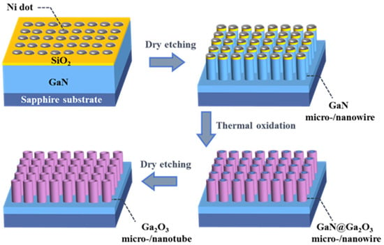
Figure 1.
Schematic illustration for the synthesis β-Ga2O3 micro/nanoarrays.
2.3. Characterizations
The surface morphology, size distribution, and chemical composition of the prepared samples were characterized by a scanning electron microscope (SEM, GeminiSEM 500) with energy dispersive spectroscopy (EDS). A high-resolution transmission electron microscope (HRTEM, Tecnai G2 F20 S-TWIN) was used to characterize the crystallographic and structural properties of β-Ga2O3 NTs samples. The preparation of TEM samples is a simple process. The NTs were first scraped from the substrate surface and dispersed in ethanol by ultrasonic agitations. Then a few droplets of the suspension were placed on a copper grid covered with a perforated carbon film and finally dried at room temperature in ambient air.
3. Results and Discussion
The vertically aligned GaN and β-Ga2O3 NW arrays were successfully fabricated by ICP etching using self-assembled Ni nanoislands as the etching masks [23]. ICP power/RF power, chamber pressure, and Cl2/BCl3 gas mixing ratio were adjusted to investigate the effect of input process parameters on the etch characteristics of GaN and β-Ga2O3 films. The etching rates of the prepared GaN and β-Ga2O3 NWs under optimized etching conditions are shown in Table 1. The results show that ICP etching of β-Ga2O3 requires higher gas flow, higher etching power, and higher chamber pressure, but the achieved etching rate is still very low, which means that β-Ga2O3 would not be etched away completely while GaN is etched rapidly under the same etching conditions.

Table 1.
ICP etch conditions studied for GaN and β-Ga2O3 nanowires.
Figure 2 shows a schematic diagram of the formation mechanism of β-Ga2O3 micro-/nanotubes based on the large etching difference between GaN and β-Ga2O3 [21,31]. The GaN@Ga2O3 micro-/nanowires are etched using the ICP etching condition for GaN to remove the GaN core while retaining the Ga2O3 shell, to prepare Ga2O3 micro-/nanotubes with a hollow structure. On the one hand, the main etching component for GaN is Cl2 of Cl2/BCl3 ICP-plasmas. For GaN, the Cl radicals in the Cl2 plasma are the main chemical reactant, which can chemically react with GaN to obtain the volatile etch product GaCl3. BCl3 can act as a wetting agent, and the BCl+3 ions and BCl+2 ions are mainly used to remove GaCl3 by physical sputtering [32,33]. However, for Ga2O3, BCl3 plasma exhibits a stronger etching effect, and Cl2 plasma exhibits a weaker etching effect [21]. BCl+2 ions react chemically with Ga2O3. B3Cl3O3 gas is produced when the oxygen pressure is lower than the critical oxygen pressure. When the oxygen pressure is higher than the critical oxygen pressure, a nonvolatile B2O3 product will be formed. The product will accumulate and form a barrier layer on the Ga2O3 surface, hindering the further etching of Ga2O3 [19,34]. On the other hand, Ga2O3 is a strongly bonded material [35], and its ICP etching requires higher gas flow and etching power. Therefore, under the conditions of ICP etching GaN, β-Ga2O3 will not be effectively etched, thus forming the β-Ga2O3 micro-/nanotubes.

Figure 2.
Schematic illustration of the formation process of β-Ga2O3 micro-/nanotube depicted as a selective etching between GaN and β-Ga2O3.
Figure 3a,d shows the SEM images of vertical GaN NW arrays on the sapphire substrate. The density of the GaN NWs is about 8.7 × 108 cm−2, and the average height and diameter are 1.6 μm and 200 nm, respectively. From Figure 3d, it can be observed that the remaining Ni/SiO2 mask layer is on the top of the GaN NWs with relatively vertical sidewall profiles. Compared with other soft masks, this mask has better anisotropic etching characteristics for GaN materials. Besides, to a certain degree, the mask layer can prevent the reaction and diffusion of O2 from the top of the NW in the subsequent thermal oxidation process.
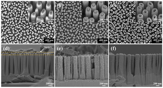
Figure 3.
SEM images (a,d) of the GaN nanowire (NW) arrays before BOE treatment. SEM images (b,e) of the GaN@Ga2O3 NW arrays oxidized at 950 °C for 10 min. SEM images (c,f) of the β-Ga2O3 NT arrays after ICP etching. The inset of (a–c) is the tilted-view SEM image.
The GaN NW array sample was thermally oxidized for 10 min in an environment with an oxygen flow of 200 sccm and a temperature of 950 °C. This process can realize the transformation of crystalline structures from GaN NWs into GaN@Ga2O3 NWs. The SEM images of GaN@Ga2O3 NWs after BOE treatment are shown in Figure 3b,e. It is observed from the figures that the NW array maintains its original shape, but its surface becomes rough after the thermal oxidation. In addition, the uniform Ga2O3 shell layer was formed on the surface of GaN NWs with an average thickness of about 60 nm (Figure 3b). The GaN@Ga2O3 NW arrays were etched under the etching process conditions for GaN (Table 1), and β-Ga2O3 NT arrays were obtained, as shown in Figure 3c,f. The inset of Figure 3c shows a magnified tilted-view SEM image of β-Ga2O3 NTs, showing a hollow internal structure, which indicates that the ICP process effectively etched the GaN core.
The grazing incidence in-plane geometry was used to determine the crystal structure of Ga2O3 grains. Figure 4 shows the in-plane diffraction patterns of unoxidized GaN nanowires and Ga2O3 nanotubes oxidized at 950 °C for 5 min, 10 min, and 15 min. The XRD reflections at 18.9°, 30.2°, 31.7°, 35.1°, 37.4°, 60.0°, and 64.7° were assigned to the beta phase of monoclinic Ga2O3 planes (−201), (400), (002), (111), (401), (−603) and (−712), respectively. The result indicates that GaN is converted to polycrystalline β-Ga2O3 after thermal oxidation treatment.
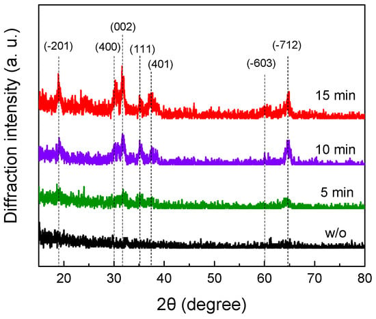
Figure 4.
Grazing incidence in-plane XRD analysis of β-Ga2O3 NTs oxidized at 950 °C and GaN NWs (w/o). Oxidation times and peak assignment are indicated in the figure.
Figure 5a shows the TEM image of β-Ga2O3 NT oxidized at 950 °C for 10 min. As expected, the cavities of the NT can be clearly seen. It can also identify a clear interface on the inner wall of the tube. The outer diameter and wall thickness of the NT is about 200 and 60 nm, respectively. The selected area electron diffraction (SAED) image is shown in Figure 5b, and the diffraction pattern indicates that the β-Ga2O3 NT is polycrystalline. From the HRTEM image in Figure 5c, the lattice spacing of approximately 0.282 nm corresponds to (002) plane of β-Ga2O3 [36]. In addition, the EDS element mapping and the line-scan images of individual NT were also performed. The yellow, red, and blue images of the EDS mapping analysis in Figure 5e illustrate the presence of Ga, N, and O elements, respectively. It can be seen that Ga and O elements are mainly distributed on the NT, while the distribution of N elements has no obvious aggregation. Figure 5f shows the EDS line-scan analysis of the marked red line area in Figure 5d. It can be seen that the peak profile of Ga and O elements is valley-shaped, the intensity on both sides is higher than the intensity at the center, and the thickness of the tube wall is about 60 nm. The content of N element is very low. These results are consistent with the TEM image and prove a hollow tubular structure.
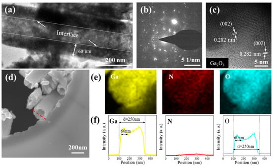
Figure 5.
(a) TEM image of a single β-Ga2O3 nanotube (NT) oxidized at 950 °C for 10 min. (b) SAED pattern and (c) HRTEM image of the β-Ga2O3 NT. (d) The SEM graph of individual Ga2O3 NT, (e) corresponding EDS elemental mapping images, and (f) EDS line scanning.
To further study the relationship between the oxidation parameters and the structure of β-Ga2O3 NTs, the GaN NWs were oxidized at different times and temperatures, and the oxygen flow rate was fixed at 200 sccm. Figure 6a–c shows the SEM images of β-Ga2O3 NT arrays prepared by oxidation at a temperature of 950 °C for 5 min, 10 min, and 15 min. It can be seen that the wall thickness of the NTs is different under different oxidation times, and the oxidation reaction of GaN starts from the surface of the NW and then gradually diffuses into the interior. Figure 6d,e shows the SEM images of β-Ga2O3 NT arrays prepared by oxidation at 850 °C and 900 °C for 15 min. When the oxidation temperature increases from 850 °C to 900 °C, the wall thickness of the NTs increases slightly. The wall thickness of the NTs increases sharply as the oxidation temperature rises to 950 °C (Figure 6c). Figure 6f shows the oxidation rate of β-Ga2O3 NTs under different oxidation conditions. The red line represents the oxidation rate of β-Ga2O3 NTs oxidized for 15 min at 850 °C, 900 °C, and 950 °C. The oxidation rate vs. temperature relationships yield linear Arrhenius plots [37], indicating that the oxidation process in the regime is under interfacial reaction-controlled. The black line represents the oxidation rate of β-Ga2O3 NTs oxidized under different oxidation times at 950 °C. The oxidation rate decreases gradually as the oxidation time increases, which means that the oxidation process may be limited by a diffusion-controlled mechanism [38,39]. It could be seen from the above experimental results that Ga2O3 NT arrays with different inner diameter wall thicknesses can be synthesized by adjusting the oxidation parameters.
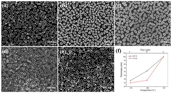
Figure 6.
SEM images of the β-Ga2O3 NT arrays prepared in different oxidation times at 950 °C for (a) 5 min, (b) 10 min, (c) 15 min. SEM images of the β-Ga2O3 NT arrays prepared in different oxidation temperatures for 15 min at (d) 850 °C and (e) 900 °C. The oxidation rate images (f) of β-Ga2O3 NTs under different oxidation conditions.
The GaN NWs etched by self-assembled Ni metal mask technology are usually unevenly distributed [40], resulting in uneven distribution of subsequent NTs. Therefore, the GaN templates were patterned by photolithography, and then periodic MT arrays with an outer diameter of about 1.7 μm were prepared using the same route. The β-Ga2O3 MT arrays prepared by oxidation for 20 min, 30 min, and 40 min in an environment at a temperature of 950 °C are shown in Figure 7. The MTs also have a hollow structure with a density of about 7 × 106 cm−2. As the oxidation time increases, the corresponding wall thicknesses are about 130 nm, 150 nm, and 155 nm, respectively (Figure 7a–c). In addition, more needle-like nanostructures appeared on the GaN surface (Figure 7d–f). GaN needle-like nanostructures tend to be formed at the defects of the GaN template. The reason is that the GaOx products migrate on the surface and accumulate to form large grains at the surface defects during the thermal oxidation [25], which serves as a mask to form needle-like nanostructures on the GaN surface during the etching process.
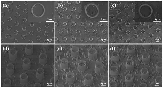
Figure 7.
Plane and tilted view SEM images of the β-Ga2O3 microtubes (MTs) samples oxidized at 950 °C for (a,d) 20 min, (b,e) 30 min, and (c,f) 40 min. Insets at the top right corner show high-magnification images of the same sample.
The above results prove the feasibility and versatility of this method for preparing vertical well-ordered tubular arrays. The periodic Ga2O3 NT arrays would be obtained by nanopatterning using e-beam or nanoimprint lithographic techniques. The method is novel and relatively simple, which can realize the control of the size, length, and wall thickness of the β-Ga2O3 tubular structure, providing possibilities for applications in catalytic, gas-sensing, optic, electronic, photochemical, and terahertz communications [17,41,42,43,44]. The hybrid micro-/nanoLEDs with high-performance red/green/blue and white emissions have been demonstrated in our previous work [45,46]. The preparation of white light LEDs integrated with β-Ga2O3 micro-/nanotubes through photolithography and selective etching route is now undergoing. A schematic of the LED device is shown in Figure 8. β-Ga2O3 micro-/nanotube arrays on the surface of InGaN/GaN MQW epitaxial wafers are prepared through a selective etching route, which replaces the nanoholes previously prepared by nanoimprint lithography technique [45]. Then the red and green quantum dots are filled into the micro-/nanotubes to blend white light sources.
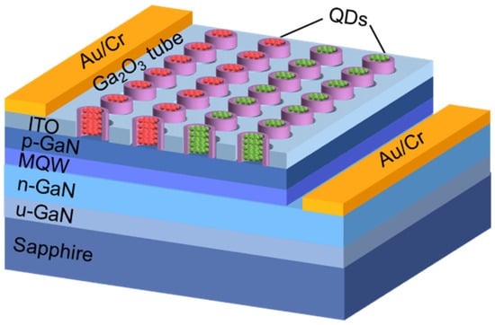
Figure 8.
Schematic of the white LED with β-Ga2O3 micro-/nanotubes.
4. Conclusions
In summary, we developed a simple selective dry etching approach to fabricate the large-scale β-Ga2O3 micro-/nanotube arrays with controllable dimensions on the GaN template. The wall thickness of the Ga2O3 tube is related to the oxidation parameters and varies with the oxidation temperature and time. Through this route, GaN@Ga2O3 micro-/nanowires with different oxide shell thicknesses were prepared by changing thermal oxidation parameters, and β-Ga2O3 micro-/nanotubes were obtained under selective dry etching. It is expected that the β-Ga2O3 micro-/nanotube arrays would be used as new materials for novel applications in optoelectronics, such as photodetectors, gas sensors, and electroluminescent devices.
Author Contributions
Conceptualization, X.X.; investigation and data curation, L.Z., S.D. and Y.L.; funding acquisition, X.X. and R.Z.; resources, X.X., Z.X., T.T., B.L., P.C., R.Z. and Y.Z.; supervision, X.X., R.Z. and Y.Z.; writing—original draft preparation, S.D.; writing—review and editing, X.X. All authors have read and agreed to the published version of the manuscript.
Funding
This research was funded by the National Key R&D Program of China (grant no. 2017YFB0404201), the State Key R&D Program of Jiangsu Province (grant no. BE2019103), the Six-Talent Peaks Project of Jiangsu Province (grant no. XCL-107).
Acknowledgments
This work is financially supported by the National Key R&D Program of China (grant no. 2017YFB0404201), the State Key R&D Program of Jiangsu Province (grant no. BE2019103), the Six-Talent Peaks Project of Jiangsu Province (grant no. XCL-107), the Fund from the Solid-state Lighting and Energy-Saving Electronics Collaborative Innovation Center, PAPD, and the Fund from the State Grid Shandong Electric Power Company.
Conflicts of Interest
The authors declare no conflict of interest.
References
- Chang, P.C.; Fan, Z.; Tseng, W.Y.; Rajagopal, A.; Lu, J.G. β-Ga2O3 nanowires: Synthesis, characterization, and p-channel field-effect transistor. Appl. Phys. Lett. 2005, 87, 222102. [Google Scholar] [CrossRef]
- Ahn, S.; Ren, F.; Kim, J.; Oh, S.; Kim, J.; Mastro, M.A.; Pearton, S.J. Effect of front and back gates on β-Ga2O3 nano-belt field-effect transistors. Appl. Phys. Lett. 2016, 109, 062102. [Google Scholar] [CrossRef]
- Chen, J.X.; Li, X.X.; Tao, J.J.; Cui, H.Y.; Huang, W.; Ji, Z.G.; Sai, Q.L.; Xia, C.T.; Lu, H.L.; Zhang, D.W. Fabrication of a Nb-Doped β-Ga2O3 Nanobelt Field-Effect Transistor and Its Low-Temperature Behavior. ACS Appl. Mater. Interfaces 2020, 12, 8437–8445. [Google Scholar] [CrossRef]
- Kim, J.; Oh, S.; Mastro, M.A.; Kim, J. Exfoliated β-Ga2O3 nano-belt field-effect transistors for air-stable high power and high temperature electronics. Phys. Chem. Chem. Phys. 2016, 18, 15760–15764. [Google Scholar] [CrossRef] [PubMed]
- Xie, C.; Lu, X.T.; Ma, M.R.; Tong, X.W.; Zhang, Z.X.; Wang, L.; Wu, C.Y.; Yang, W.H.; Luo, L.B. Catalyst-Free Vapor-Solid Deposition Growth of β-Ga2O3 Nanowires for DUV Photodetector and Image Sensor Application. Adv. Opt. Mater. 2019, 7, 1901257. [Google Scholar] [CrossRef]
- He, C.; Guo, D.; Chen, K.; Wang, S.; Shen, J.; Zhao, N.; Liu, A.; Zheng, Y.; Li, P.; Wu, Z.; et al. α-Ga2O3 Nanorod Array-Cu2O Microsphere p-n Junctions for Self-Powered Spectrum-Distinguishable Photodetectors. ACS Appl. Nano Mater. 2019, 2, 4095–4103. [Google Scholar] [CrossRef]
- Chen, M.; Zhao, B.; Hu, G.; Fang, X.; Wang, H.; Wang, L.; Luo, J.; Han, X.; Wang, X.; Pan, C.; et al. Piezo-Phototronic Effect Modulated Deep UV Photodetector Based on ZnO-Ga2O3 Heterojuction Microwire. Adv. Funct. Mater. 2018, 28, 1706379. [Google Scholar] [CrossRef]
- Rex, J.P.; Kwong, Y.F.; San, L.H. The influence of deposition temperature on the structural, morphological and optical properties of micro-size structures of beta-Ga2O3. Results Phys. 2019, 14, 102475. [Google Scholar] [CrossRef]
- Bui, Q.C.; Largeau, L.; Morassi, M.; Jegenyes, N.; Mauguin, O.; Travers, L.; Lafosse, X.; Dupuis, C.; Harmand, J.C.; Tchernycheva, M.; et al. GaN/Ga2O3 Core/Shell Nanowires Growth: Towards High Response Gas Sensors. Appl. Sci. 2019, 9, 3528. [Google Scholar] [CrossRef] [Green Version]
- Jang, Y.G.; Kim, W.S.; Kim, D.H.; Hong, S.H. Fabrication of Ga2O3/SnO2 core–shell nanowires and their ethanol gas sensing properties. J. Mater. Res. 2011, 26, 2322–2327. [Google Scholar] [CrossRef]
- Chandiran, A.K.; Tetreault, N.; Humphry-Baker, R.; Kessler, F.; Baranoff, E.; Yi, C.; Nazeeruddin, M.K.; Grätzel, M. Subnanometer Ga2O3 Tunnelling Layer by Atomic Layer Deposition to Achieve 1.1 V Open-Circuit Potential in Dye-Sensitized Solar Cells. Nano Lett. 2012, 12, 3941–3947. [Google Scholar] [CrossRef] [PubMed]
- Hsieh, C.H.; Chou, L.J.; Lin, G.R.; Bando, Y.; Golberg, D. Nanophotonic Switch: Gold-in-Ga2O3 Peapod Nanowires. Nano Lett. 2008, 8, 3081–3085. [Google Scholar] [CrossRef]
- Cheng, B.; Samulski, E.T. Fabrication and characterization of nanotubular semiconductor oxides In2O3 and Ga2O3. J. Mater. Chem. 2001, 11, 2901–2902. [Google Scholar] [CrossRef]
- Zhang, Y.; Yang, J.; Li, Q.; Cao, X. Preparation of Ga2O3 nanoribbons and tubes by electrospinning. J. Cryst. Growth 2007, 308, 180–184. [Google Scholar] [CrossRef]
- Gong, N.W.; Lu, M.Y.; Wang, C.Y.; Chen, Y.; Chen, L.J. Au(Si)-filled β-Ga2O3 nanotubes as wide range high temperature nanothermometers. Appl. Phys. Lett. 2008, 92, 073101. [Google Scholar] [CrossRef]
- Jiang, H.; Chen, Y.; Zhou, Q.; Su, Y.; Xiao, H.; Zhu, L. Temperature dependence of Ga2O3 micro/nanostructures via vapor phase growth. Mater. Chem. Phys. 2007, 103, 14–18. [Google Scholar] [CrossRef]
- Braniste, T.; Dragoman, M.; Zhukov, S.; Aldrigo, M.; Ciobanu, V.; Iordanescu, S.; Alyabyeva, L.; Fumagalli, F.; Ceccone, G.; Raevschi, S.; et al. Aero-Ga2O3 Nanomaterial Electromagnetically Transparent from Microwaves to Terahertz for Internet of Things Applications. Nanomaterials 2020, 10, 1047. [Google Scholar] [CrossRef]
- Liang, H.; Chen, Y.; Xia, X.; Zhang, C.; Shen, R.; Liu, Y.; Luo, Y.; Du, G. A preliminary study of SF6 based inductively coupled plasma etching techniques for beta gallium trioxide thin film. Mater. Sci. Semicond. Proc. 2015, 39, 582–586. [Google Scholar] [CrossRef]
- Hogan, J.E.; Kaun, S.W.; Ahmadi, E.; Oshima, Y.; Speck, J.S. Chlorine-based dry etching of β-Ga2O3. Semicond. Sci. Technol. 2016, 31, 065006. [Google Scholar] [CrossRef]
- Yang, J.; Ahn, S.; Ren, F.; Pearton, S.; Khanna, R.; Bevlin, K.; Geerpuram, D.; Kuramata, A. Inductively coupled plasma etching of bulk, single-crystal Ga2O3. J. Vac. Sci. Technol. B 2017, 35, 031205. [Google Scholar] [CrossRef]
- Shah, A.P.; Bhattacharya, A. Inductively coupled plasma reactive-ion etching of β-Ga2O3: Comprehensive investigation of plasma chemistry and temperature. J. Vac. Sci. Technol. A 2017, 35, 041301. [Google Scholar] [CrossRef]
- Lin, Z.; Xiu, X.; Zhang, S.; Hua, X.; Xie, Z.; Zhang, R.; Han, P.; Zheng, Y. Arrays of GaN nano-pillars fabricated by nickel nano-island mask. Mater. Lett. 2013, 108, 250–252. [Google Scholar] [CrossRef]
- Zhang, L.; Xiu, X.; Li, Y.; Zhu, Y.; Hua, X.; Xie, Z.; Tao, T.; Liu, B.; Chen, P.; Zhang, R.; et al. Solar-blind ultraviolet photodetector based on vertically aligned single-crystalline β-Ga2O3 nanowire arrays. Nanophotonics 2020, 9, 4497–4503. [Google Scholar] [CrossRef]
- Wang, S.; Li, Y.W.; Xiu, X.Q.; Zhang, L.Y.; Hua, X.M.; Xie, Z.L.; Tao, T.; Liu, B.; Chen, P.; Zhang, R.; et al. Synthesis and characterization of β-Ga2O3@GaN nanowires. Chin. Phys. B 2019, 28, 028104. [Google Scholar] [CrossRef]
- Yamada, T.; Ito, J.; Asahara, R.; Watanabe, K.; Nozaki, M.; Nakazawa, S.; Anda, Y.; Ishida, M.; Ueda, T.; Yoshigoe, A.; et al. Comprehensive study on initial thermal oxidation of GaN (0001) surface and subsequent oxide growth in dry oxygen ambient. J. Appl. Phys. 2017, 121, 035303. [Google Scholar] [CrossRef]
- Choi, J.H.; Ham, M.H.; Lee, W.; Myoung, J.M. Fabrication and characterization of GaN/amorphous Ga2O3 nanocables through thermal oxidation. Solid State Commun. 2007, 142, 437–440. [Google Scholar] [CrossRef]
- Zhang, L.; Li, Y.; Xiu, X.; Xin, G.; Xie, Z.; Tao, T.; Liu, B.; Chen, P.; Zhang, R.; Zheng, Y. Preparation of vertically aligned GaN@Ga2O3 core-shell heterostructured nanowire arrays and their photocatalytic activity for degradation of Rhodamine B. Superlattices Microstruct. 2020, 143, 106556. [Google Scholar] [CrossRef]
- Xie, Z.; Zhou, Y.; Song, L.; Liu, B.; Hua, X.; Xiu, X.; Zhang, R.; Zheng, Y. Structural properties of GaN(0001) epitaxial layers revealed by high resolution X-ray diffraction. Sci. China-Phys. Mech. Astron. 2010, 1, 68–71. [Google Scholar] [CrossRef]
- Yang, G.F.; Chen, P.; Wu, Z.L.; Yu, Z.G.; Zhao, H.; Liu, B.; Hua, X.M.; Xie, Z.L.; Xiu, X.Q.; Han, P.; et al. Characteristics of GaN thin films by inductively coupled plasma etching with Cl2/BCl3 and Cl2/Ar. J. Mater. Sci.-Mater. Electron. 2012, 23, 1224–1228. [Google Scholar] [CrossRef]
- Yang, G.F.; Chen, P.; Yu, Z.G.; Liu, B.; Xie, Z.L.; Xiu, X.Q.; Han, P.; Zhao, H.; Hua, X.M.; Zhang, R.; et al. Fabrication of GaN Nanocolumns with Semipolar Plane Using Ni Nano-Island Masks. Semicond. Technol. 2011, 36, 417–420. [Google Scholar]
- Kim, H.S.; Yeom, G.Y.; Lee, J.W.; Kim, T.I. Characteristics of inductively coupled Cl2/BCl3 plasmas during GaN etching. J. Vac. Sci. Technol. A 1999, 17, 2214–2219. [Google Scholar] [CrossRef] [Green Version]
- Tripathy, S.; Ramam, A.; Chua, S.J.; Pan, J.S.; Huan, A. Characterization of inductively coupled plasma etched surface of GaN using chemistry. J. Vac. Sci. Technol. A 2001, 19, 2522–2532. [Google Scholar] [CrossRef]
- Lee, Y.H.; Sung, Y.J.; Yeom, G.Y.; Lee, J.W.; Kim, T.I. Magnetized inductively coupled plasma etching of GaN in Cl2/BCl3 plasmas. J. Vac. Sci. Technol. A 2000, 18, 1390–1394. [Google Scholar] [CrossRef]
- McNevin, S.C. A thermochemical model for the plasma etching of aluminum in BCl3/Cl2 and BBr3/Br2. J. Vac. Sci. Technol. B 1990, 8, 1212–1222. [Google Scholar] [CrossRef]
- Pearton, S.J.; Yang, J.; Cary, P.H.; Ren, F.; Kim, J.; Tadjer, M.J.; Mastro, M.A. A review of Ga2O3 materials, processing, and devices. Appl. Phys. Rev. 2018, 5, 011301. [Google Scholar] [CrossRef] [Green Version]
- Dai, L.; You, L.P.; Duan, X.F.; Lian, W.C.; Qin, G.G. Synthesis of Ga2O3 chains with closely spaced knots connected by nanowires. J. Cryst. Growth 2004, 267, 538–542. [Google Scholar] [CrossRef]
- Brauner, N.; Shacham, M. Statistical analysis of linear and nonlinear correlation of the Arrhenius equation constants. Chem. Eng. Process. 1997, 36, 243–249. [Google Scholar] [CrossRef]
- Ham, M.H.; Lee, S.; Myoung, J.M.; Lee, W. Controlled Formation of Oxide Shells from GaN Nanowires: Poly- to Single-Crystal. Electron. Mater. Lett. 2011, 7, 243–247. [Google Scholar] [CrossRef]
- Chen, P.; Zhang, R.; Xu, X.F.; Chen, Z.Z.; Zhou, Y.G.; Xie, S.Y.; Shi, Y.; Shen, B.; Gu, S.L.; Huang, Z.C.; et al. Oxidation of gallium nitride epilayers in dry oxygen. Mater. Res. Soc. Internet J. Nitride Semicond. Res. 2000, 5, 866–872. [Google Scholar] [CrossRef] [Green Version]
- Hsieh, M.Y.; Wang, C.Y.; Chen, L.Y.; Ke, M.Y.; Huang, J. InGaN-GaN Nanorod Light Emitting Arrays Fabricated by Silica Nanomasks. IEEE J. Quantum Electron. 2008, 44, 468–472. [Google Scholar] [CrossRef]
- Lin, J.; Zong, R.; Zhou, M.; Zhu, Y. Photoelectric catalytic degradation of methylene blue by C60-modified TiO2 nanotube array. Appl. Catal. B Environ. 2009, 89, 425–431. [Google Scholar] [CrossRef]
- Hsueh, T.J.; Chang, S.J.; Hsu, C.L.; Lin, Y.R.; Chen, I.C. ZnO Nanotube Ethanol Gas Sensors. J. Electrochem. Soc. 2008, 155, K152–K155. [Google Scholar] [CrossRef]
- Star, A.; Lu, Y.; Bradley, K.; Grüner, G. Nanotube Optoelectronic Memory Devices. Nano Lett. 2004, 4, 1587–1591. [Google Scholar] [CrossRef]
- Han, J.; Liu, Z.; Guo, K.; Wang, B.; Zhang, X.; Hong, T. High-efficiency photoelectrochemical electrodes based on ZnIn2S4 sensitized ZnO nanotube arrays. Appl. Catal. B Environ. 2015, 163, 179–188. [Google Scholar] [CrossRef]
- Zhuang, Z.; Guo, X.; Liu, B.; Hu, F.R.; Li, Y.; Tao, T.; Dai, J.P.; Zhi, T.; Xie, Z.L.; Chen, P.; et al. High Color Rendering Index Hybrid III-Nitride/Nanocrystals White Light-Emitting Diodes. Adv. Funct. Mater. 2016, 26, 36–43. [Google Scholar] [CrossRef]
- Liu, B.; Chen, D.; Lu, H.; Tao, T.; Zhuang, Z.; Shao, Z.; Xu, W.; Ge, H.; Zhi, T.; Ren, F.; et al. Hybrid Light Emitters and UV Solar-Blind Avalanche Photodiodes based on III-Nitride Semiconductors. Adv. Mater. 2020, 32, 1904354. [Google Scholar] [CrossRef] [PubMed]
Publisher’s Note: MDPI stays neutral with regard to jurisdictional claims in published maps and institutional affiliations. |
© 2021 by the authors. Licensee MDPI, Basel, Switzerland. This article is an open access article distributed under the terms and conditions of the Creative Commons Attribution (CC BY) license (https://creativecommons.org/licenses/by/4.0/).