
Recent Advances in Electrical Doping of 2D Semiconductor Materials: Methods, Analyses, and Applications


Abstract
1. Introduction
2. Graphene Doping
2.1. Background
2.2. Substitutional Doping
2.3. Chemical Doping
2.4. Charge Transfer Method (Molecular Doping)
3. TMD Doping
3.1. Background
3.2. Substitutional Doping
3.3. Molecular Doping
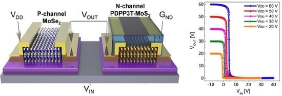
3.4. Applications
4. Conclusions and Outlook
Funding
Conflicts of Interest
References
- Rai, A.; Valsaraj, A.; Movva, H.C.; Roy, A.; Ghosh, R.; Sonde, S.; Kang, S.; Chang, J.; Trivedi, T.; Dey, R. Air stable doping and intrinsic mobility enhancement in monolayer molybdenum disulfide by amorphous titanium suboxide encapsulation. Nano Lett. 2015, 15, 4329–4336. [Google Scholar] [CrossRef]
- Kiriya, D.; Tosun, M.; Zhao, P.; Kang, J.S.; Javey, A. Air-stable surface charge transfer doping of MoS2 by benzyl viologen. J. Am. Chem. Soc. 2014, 136, 7853–7856. [Google Scholar] [CrossRef]
- McDonnell, S.; Addou, R.; Buie, C.; Wallace, R.M.; Hinkle, C.L. Defect-dominated doping and contact resistance in MoS2. ACS Nano 2014, 8, 2880–2888. [Google Scholar] [CrossRef]
- Kang, D.H.; Kim, M.S.; Shim, J.; Jeon, J.; Park, H.Y.; Jung, W.S.; Yu, H.Y.; Pang, C.H.; Lee, S.; Park, J.H. High-performance transition metal dichalcogenide photodetectors enhanced by self-assembled monolayer doping. Adv. Funct. Mater. 2015, 25, 4219–4227. [Google Scholar] [CrossRef]
- Li, Y.; Xu, C.-Y.; Hu, P.; Zhen, L. Carrier control of MoS2 nanoflakes by functional self-assembled monolayers. ACS Nano 2013, 7, 7795–7804. [Google Scholar] [CrossRef] [PubMed]
- Lee, W.H.; Park, Y.D. Tuning Electrical Properties of 2D Materials by Self-Assembled Monolayers. Adv. Mater. Interfaces 2018, 5, 1700316. [Google Scholar] [CrossRef]
- Kang, D.-H.; Jeon, M.H.; Jang, S.K.; Choi, W.-Y.; Kim, K.N.; Kim, J.; Lee, S.; Yeom, G.Y.; Park, J.-H. Self-assembled layer (SAL)-based doping on black phosphorus (BP) transistor and photodetector. ACS Photonics 2017, 4, 1822–1830. [Google Scholar] [CrossRef]
- Geim, A.K. Graphene: Status and prospects. Science 2009, 324, 1530–1534. [Google Scholar] [CrossRef]
- Miao, F.; Wijeratne, S.; Zhang, Y.; Coskun, U.; Bao, W.; Lau, C. Phase-coherent transport in graphene quantum billiards. Science 2007, 317, 1530–1533. [Google Scholar] [CrossRef]
- Morozov, S.V.; Novoselov, K.S.; Katsnelson, M.; Schedin, F.; Ponomarenko, L.; Jiang, D.; Geim, A.K. Strong suppression of weak localization in graphene. Phys. Rev. Lett. 2006, 97, 016801. [Google Scholar] [CrossRef]
- Guo, B.; Fang, L.; Zhang, B.; Gong, J.R. Graphene doping: A review. Sci. J. 2011, 1, 80–89. [Google Scholar] [CrossRef]
- Lee, H.; Paeng, K.; Kim, I.S. A review of doping modulation in graphene. Synth. Met. 2018, 244, 36–47. [Google Scholar] [CrossRef]
- Shen, X.; Liu, Y.; Pang, Y.; Yao, W. Conjugation of graphene on Au surface by π–π interaction and click chemistry. Electrochem. Commun. 2013, 30, 13–16. [Google Scholar] [CrossRef]
- Kumar, C.V.; Pattammattel, A. Introduction to Graphene: Chemical and Biochemical Applications; Elsevier: Amsterdam, The Netherlands, 2017. [Google Scholar]
- Brownlie, L.; Shapter, J. Advances in carbon nanotube n-type doping: Methods, analysis and applications. Carbon 2018, 126, 257–270. [Google Scholar] [CrossRef]
- Oh, J.S.; Kim, K.N.; Yeom, G.Y. Graphene doping methods and device applications. J. Nanosci. Nanotechnol. 2014, 14, 1120–1133. [Google Scholar] [CrossRef] [PubMed]
- Hemasiri, B.W.; Kim, J.-K.; Lee, J.-M. Fabrication of highly conductive graphene/ITO transparent bi-film through CVD and organic additives-free sol-gel techniques. Sci. Rep. 2017, 7, 17868. [Google Scholar] [CrossRef]
- Xue, Y.; Wu, B.; Bao, Q.; Liu, Y. Controllable synthesis of doped graphene and its applications. Small 2014, 10, 2975–2991. [Google Scholar] [CrossRef]
- Warner, J.H.; Schaffel, F.; Rummeli, M.; Bachmatiuk, A. Graphene: Fundamentals and Emergent Applications; Newnes: London, UK, 2012. [Google Scholar]
- Sood, A.K.; Lund, I.; Puri, Y.R.; Efstathiadis, H.; Haldar, P.; Dhar, N.K.; Lewis, J.; Dubey, M.; Zakar, E.; Wijewarnasuriya, P. Review of graphene technology and its applications for electronic devices. Graphene New Trends Dev. 2015. [Google Scholar] [CrossRef]
- Saha, S.K.; Chandrakanth, R.C.; Krishnamurthy, H.; Waghmare, U. Mechanisms of molecular doping of graphene: A first-principles study. Phys. Rev. B 2009, 80, 155414. [Google Scholar] [CrossRef]
- Chaves, A.; Azadani, A.G.; Alsalman, H.; da Costa, D.R.; Frisenda, R.; Chaves, A.J.; Song, S.H.; Kim, Y.D.; He, D.; Zhou, J.; et al. Bandgap engineering of two-dimensional semiconductor materials. NPJ 2D Mater. Appl. 2020, 4, 29. [Google Scholar] [CrossRef]
- Agnoli, S.; Favaro, M. Doping graphene with boron: A review of synthesis methods, physicochemical characterization, and emerging applications. J. Mater. Chem. A 2016, 4, 5002–5025. [Google Scholar] [CrossRef]
- Santhosh, N.M.; Filipič, G.; Kovacevic, E.; Jagodar, A.; Berndt, J.; Strunskus, T.; Kondo, H.; Hori, M.; Tatarova, E.; Cvelbar, U. N-graphene nanowalls via plasma nitrogen incorporation and substitution: The experimental evidence. Nano-Micro Lett. 2020, 12, 53. [Google Scholar] [CrossRef]
- Wang, X.; Sun, G.; Routh, P.; Kim, D.-H.; Huang, W.; Chen, P. Heteroatom-doped graphene materials: Syntheses, properties and applications. Chem. Soc. Rev. 2014, 43, 7067–7098. [Google Scholar] [CrossRef] [PubMed]
- Liu, H.; Liu, Y.; Zhu, D. Chemical doping of graphene. J. Mater. Chem. 2011, 21, 3335–3345. [Google Scholar] [CrossRef]
- Manojkumar, P.; Krishna, N.G.; Mangamma, G.; Albert, S. Understanding the structural and chemical changes in vertical graphene nanowalls upon plasma nitrogen ion implantation. Phys. Chem. Chem. Phys. 2019, 21, 10773–10783. [Google Scholar] [CrossRef]
- Hojati-Talemi, P.; Simon, G.P. Field emission study of graphene nanowalls prepared by microwave-plasma method. Carbon 2011, 49, 2875–2877. [Google Scholar] [CrossRef]
- Lee, V.; Dennis, R.V.; Schultz, B.J.; Jaye, C.; Fischer, D.A.; Banerjee, S. Soft X-ray absorption spectroscopy studies of the electronic structure recovery of graphene oxide upon chemical defunctionalization. J. Phys. Chem. C 2012, 116, 20591–20599. [Google Scholar] [CrossRef]
- Girard-Lauriault, P.-L.; Illgen, R.; Ruiz, J.-C.; Wertheimer, M.R.; Unger, W.E. Surface functionalization of graphite and carbon nanotubes by vacuum-ultraviolet photochemical reactions. Appl. Surf. Sci. 2012, 258, 8448–8454. [Google Scholar] [CrossRef]
- Rybin, M.; Pereyaslavtsev, A.; Vasilieva, T.; Myasnikov, V.; Sokolov, I.; Pavlova, A.; Obraztsova, E.; Khomich, A.; Ralchenko, V.; Obraztsova, E. Efficient nitrogen doping of graphene by plasma treatment. Carbon 2016, 96, 196–202. [Google Scholar] [CrossRef]
- Banhart, F.; Kotakoski, J.; Krasheninnikov, A.V. Structural defects in graphene. ACS Nano 2011, 5, 26–41. [Google Scholar] [CrossRef]
- Farmer, D.B.; Golizadeh-Mojarad, R.; Perebeinos, V.; Lin, Y.-M.; Tulevski, G.S.; Tsang, J.C.; Avouris, P. Chemical doping and electron−hole conduction asymmetry in graphene devices. Nano Lett. 2009, 9, 388–392. [Google Scholar] [CrossRef]
- Abdullah-Al-Galib, M.; Hou, B.; Shahriad, T.; Zivanovic, S.; Radadia, A.D. Stability of few layer graphene films doped with gold (III) chloride. Appl. Surf. Sci. 2016, 366, 78–84. [Google Scholar] [CrossRef]
- Shin, H.-J.; Choi, W.M.; Choi, D.; Han, G.H.; Yoon, S.-M.; Park, H.-K.; Kim, S.-W.; Jin, Y.W.; Lee, S.Y.; Kim, J.M. Control of electronic structure of graphene by various dopants and their effects on a nanogenerator. J. Am. Chem. Soc. 2010, 132, 15603–15609. [Google Scholar] [CrossRef]
- Gunes, F.; Shin, H.-J.; Biswas, C.; Han, G.H.; Kim, E.S.; Chae, S.J.; Choi, J.-Y.; Lee, Y.H. Layer-by-layer doping of few-layer graphene film. ACS Nano 2010, 4, 4595–4600. [Google Scholar] [CrossRef]
- Kwon, K.C.; Choi, K.S.; Kim, S.Y. Increased work function in few-layer graphene sheets via metal chloride doping. Adv. Funct. Mater. 2012, 22, 4724–4731. [Google Scholar] [CrossRef]
- Kwon, K.C.; Kim, B.J.; Lee, J.-L.; Kim, S.Y. Effect of anions in Au complexes on doping and degradation of graphene. J. Mater. Chem. C 2013, 1, 2463–2469. [Google Scholar] [CrossRef]
- Jeong, H.K.; Kim, K.-J.; Kim, S.M.; Lee, Y.H. Modification of the electronic structures of graphene by viologen. Chem. Phys. Lett. 2010, 498, 168–171. [Google Scholar] [CrossRef]
- Krishnamurthy, S.; Lightcap, I.V.; Kamat, P.V. Electron transfer between methyl viologen radicals and graphene oxide: Reduction, electron storage and discharge. J. Photochem. Photobiol. A Chem. 2011, 221, 214–219. [Google Scholar] [CrossRef]
- Al-Mumen, H.; Dong, L.; Li, W. SU-8 doped and encapsulated n-type graphene nanomesh with high air stability. Appl. Phys. Lett. 2013, 103, 232113. [Google Scholar] [CrossRef]
- Al-Mumen, H. Characterisation of SU-8 n-doping carbon nanotube-based electronic devices. Micro Nano Lett. 2015, 10, 670–673. [Google Scholar] [CrossRef]
- Wehling, T.; Novoselov, K.; Morozov, S.; Vdovin, E.; Katsnelson, M.; Geim, A.; Lichtenstein, A. Molecular doping of graphene. Nano Lett. 2008, 8, 173–177. [Google Scholar] [CrossRef]
- Chen, W.; Qi, D.; Gao, X.; Wee, A.T.S. Surface transfer doping of semiconductors. Prog. Surf. Sci. 2009, 84, 279–321. [Google Scholar] [CrossRef]
- Tsetseris, L.; Pantelides, S.T. Molecular doping of graphene with ammonium groups. Phys. Rev. B 2012, 85, 155446. [Google Scholar] [CrossRef]
- Singh, A.; Uddin, M.; Tolson, J.; Maire-Afeli, H.; Sbrockey, N.; Tompa, G.; Spencer, M.; Vogt, T.; Sudarshan, T.; Koley, G. Electrically tunable molecular doping of graphene. Appl. Phys. Lett. 2013, 102, 043101. [Google Scholar] [CrossRef]
- Park, J.; Jo, S.B.; Yu, Y.J.; Kim, Y.; Yang, J.W.; Lee, W.H.; Kim, H.H.; Hong, B.H.; Kim, P.; Cho, K. Single-gate bandgap opening of bilayer graphene by dual molecular doping. Adv. Mater. 2012, 24, 407–411. [Google Scholar] [CrossRef]
- Pinto, H.; Jones, R.; Goss, J.; Briddon, P. p-type doping of graphene with F4-TCNQ. J. Phys. Condens. Matter 2009, 21, 402001. [Google Scholar] [CrossRef] [PubMed]
- Ishikawa, R.; Bando, M.; Morimoto, Y.; Sandhu, A. Doping graphene films via chemically mediated charge transfer. Nanoscale Res. Lett. 2011, 6, 111. [Google Scholar] [CrossRef]
- Lee, W.H.; Suk, J.W.; Lee, J.; Hao, Y.; Park, J.; Yang, J.W.; Ha, H.-W.; Murali, S.; Chou, H.; Akinwande, D. Simultaneous transfer and doping of CVD-grown graphene by fluoropolymer for transparent conductive films on plastic. ACS Nano 2012, 6, 1284–1290. [Google Scholar] [CrossRef]
- Pandey, S.K.; Alsalman, H.; Azadani, J.G.; Izquierdo, N.; Low, T.; Campbell, S.A. Controlled p-type substitutional doping in large-area monolayer WSe2 crystals grown by chemical vapor deposition. Nanoscale 2018, 10, 21374–21385. [Google Scholar] [CrossRef]
- Zhang, K.; Bersch, B.M.; Joshi, J.; Addou, R.; Cormier, C.R.; Zhang, C.; Xu, K.; Briggs, N.C.; Wang, K.; Subramanian, S. Tuning the electronic and photonic properties of monolayer MoS2 via in situ rhenium substitutional doping. Adv. Funct. Mater. 2018, 28, 1706950. [Google Scholar] [CrossRef]
- Kim, Y.; Bark, H.; Kang, B.; Lee, C. Wafer-scale substitutional doping of monolayer MoS2 films for high-performance optoelectronic devices. ACS Appl. Mater. Interfaces 2019, 11, 12613–12621. [Google Scholar] [CrossRef]
- Yue, Y.; Jiang, C.; Han, Y.; Wang, M.; Ren, J.; Wu, Y. Magnetic anisotropies of Mn-, Fe-, and Co-doped monolayer MoS2. J. Magn. Magn. Mater. 2020, 496, 165929. [Google Scholar] [CrossRef]
- Jin, Y.; Zeng, Z.; Xu, Z.; Lin, Y.-C.; Bi, K.; Shao, G.; Hu, T.S.; Wang, S.; Li, S.; Suenaga, K. Synthesis and transport properties of degenerate p-type Nb-doped WS2 monolayers. Chem. Mater. 2019, 31, 3534–3541. [Google Scholar] [CrossRef]
- Zhang, P.; Cheng, N.; Li, M.; Zhou, B.; Bian, C.; Wei, Y.; Wang, X.; Jiang, H.; Bao, L.; Lin, Y. Transition-Metal Substitution-Induced Lattice Strain and Electrical Polarity Reversal in Monolayer WS2. ACS Appl. Mater. Interfaces 2020, 12, 18650–18659. [Google Scholar] [CrossRef]
- Chang, R.-J.; Sheng, Y.; Ryu, G.H.; Mkhize, N.; Chen, T.; Lu, Y.; Chen, J.; Lee, J.K.; Bhaskaran, H.; Warner, J.H. Postgrowth Substitutional Tin Doping of 2D WS2 Crystals Using Chemical Vapor Deposition. ACS Appl. Mater. Interfaces 2019, 11, 24279–24288. [Google Scholar] [CrossRef]
- Gao, H.; Suh, J.; Cao, M.C.; Joe, A.Y.; Mujid, F.; Lee, K.-H.; Xie, S.; Poddar, P.; Lee, J.-U.; Kang, K. Tuning electrical conductance of MoS2 monolayers through substitutional doping. Nano Lett. 2020, 20, 4095–4101. [Google Scholar] [CrossRef]
- Zhang, T.; Fujisawa, K.; Zhang, F.; Liu, M.; Lucking, M.C.; Gontijo, R.N.; Lei, Y.; Liu, H.; Crust, K.; Granzier-Nakajima, T. Universal in situ substitutional doping of transition metal dichalcogenides by liquid-phase precursor-assisted synthesis. ACS Nano 2020, 14, 4326–4335. [Google Scholar] [CrossRef]
- Kanade, C.; Arbuj, S.; Kanade, K.; Kim, K.S.; Yeom, G.Y.; Kim, T.; Kale, B. Hierarchical nanostructures of nitrogen-doped molybdenum sulphide for supercapacitors. RSC Adv. 2018, 8, 39749–39755. [Google Scholar] [CrossRef]
- Zhao, B.; Liu, L.; Cheng, G.; Li, T.; Qi, N.; Chen, Z.; Tang, Z. Interaction of O2 with monolayer MoS2: Effect of doping and hydrogenation. Mater. Des. 2017, 113, 1–8. [Google Scholar] [CrossRef]
- Yang, L.; Majumdar, K.; Liu, H.; Du, Y.; Wu, H.; Hatzistergos, M.; Hung, P.; Tieckelmann, R.; Tsai, W.; Hobbs, C. Chloride molecular doping technique on 2D materials: WS2 and MoS2. Nano Lett. 2014, 14, 6275–6280. [Google Scholar] [CrossRef]
- Tang, B.; Yu, Z.G.; Huang, L.; Chai, J.; Wong, S.L.; Deng, J.; Yang, W.; Gong, H.; Wang, S.; Ang, K.-W. Direct n-to p-type channel conversion in monolayer/few-layer WS2 field-effect transistors by atomic nitrogen treatment. ACS Nano 2018, 12, 2506–2513. [Google Scholar] [CrossRef]
- Kim, K.H.; Kim, K.S.; Ji, Y.J.; Moon, I.; Heo, K.; Kang, D.-H.; Kim, K.N.; Yoo, W.J.; Park, J.-H.; Yeom, G.Y. Effect of large work function modulation of MoS 2 by controllable chlorine doping using a remote plasma. J. Mater. Chem. C 2020, 8, 1846–1851. [Google Scholar] [CrossRef]
- Liang, Q.; Gou, J.; Zhang, Q.; Zhang, W.; Wee, A.T.S. Oxygen-induced controllable p-type doping in 2D semiconductor transition metal dichalcogenides. Nano Res. 2020, 13, 3439–3444. [Google Scholar] [CrossRef]
- Komsa, H.-P.; Kotakoski, J.; Kurasch, S.; Lehtinen, O.; Kaiser, U.; Krasheninnikov, A.V. Two-dimensional transition metal dichalcogenides under electron irradiation: Defect production and doping. Phys. Rev. Lett. 2012, 109, 035503. [Google Scholar] [CrossRef] [PubMed]
- Kang, D.-H.; Dugasani, S.R.; Park, H.-Y.; Shim, J.; Gnapareddy, B.; Jeon, J.; Lee, S.; Roh, Y.; Park, S.H.; Park, J.-H. Ultra-low doping on two-dimensional transition metal dichalcogenides using DNA nanostructure doped by a combination of lanthanide and metal ions. Sci. Rep. 2016, 6, 20333. [Google Scholar] [CrossRef]
- Du, Y.; Liu, H.; Neal, A.T.; Si, M.; Peide, D.Y. Molecular Doping of Multilayer MOS2 Field-Effect Transistors: Reduction in Sheet and Contact Resistances. IEEE Electron. Device Lett. 2013, 34, 1328–1330. [Google Scholar] [CrossRef]
- Lockhart de la Rosa, C.J.; Phillipson, R.; Teyssandier, J.; Adisoejoso, J.; Balaji, Y.; Huyghebaert, C.; Radu, I.; Heyns, M.; De Feyter, S.; De Gendt, S. Molecular doping of MoS2 transistors by self-assembled oleylamine networks. Appl. Phys. Lett. 2016, 109, 253112. [Google Scholar] [CrossRef]
- Bertolazzi, S.; Gobbi, M.; Zhao, Y.; Backes, C.; Samorì, P. Molecular chemistry approaches for tuning the properties of two-dimensional transition metal dichalcogenides. Chem. Soc. Rev. 2018, 47, 6845–6888. [Google Scholar] [CrossRef]
- Xu, K.; Wang, Y.; Zhao, Y.; Chai, Y. Modulation doping of transition metal dichalcogenide/oxide heterostructures. J. Mater. Chem. C 2017, 5, 376–381. [Google Scholar] [CrossRef]
- Cai, Y.; Zhou, H.; Zhang, G.; Zhang, Y.-W. Modulating carrier density and transport properties of MoS2 by organic molecular doping and defect engineering. Chem. Mater. 2016, 28, 8611–8621. [Google Scholar] [CrossRef]
- Cho, Y.; Park, J.H.; Kim, M.; Jeong, Y.; Yu, S.; Lim, J.Y.; Yi, Y.; Im, S. Impact of organic molecule-induced charge transfer on operating voltage control of both n-MoS2 and p-MoTe2 transistors. Nano Lett. 2019, 19, 2456–2463. [Google Scholar] [CrossRef] [PubMed]
- Lim, J.Y.; Pezeshki, A.; Oh, S.; Kim, J.S.; Lee, Y.T.; Yu, S.; Hwang, D.K.; Lee, G.H.; Choi, H.J.; Im, S. Homogeneous 2D MoTe2 p–n Junctions and CMOS Inverters formed by Atomic-Layer-Deposition-Induced Doping. Adv. Mater. 2017, 29, 1701798. [Google Scholar] [CrossRef]
- Fang, H.; Tosun, M.; Seol, G.; Chang, T.C.; Takei, K.; Guo, J.; Javey, A. Degenerate n-doping of few-layer transition metal dichalcogenides by potassium. Nano Lett. 2013, 13, 1991–1995. [Google Scholar] [CrossRef]
- Sim, D.M.; Kim, M.; Yim, S.; Choi, M.-J.; Choi, J.; Yoo, S.; Jung, Y.S. Controlled doping of vacancy-containing few-layer MoS2 via highly stable thiol-based molecular chemisorption. ACS Nano 2015, 9, 12115–12123. [Google Scholar] [CrossRef]
- Benjamin, C.J.; Zhang, S.; Chen, Z. Controlled doping of transition metal dichalcogenides by metal work function tuning in phthalocyanine compounds. Nanoscale 2018, 10, 5148–5153. [Google Scholar] [CrossRef]
- Mouri, S.; Miyauchi, Y.; Matsuda, K. Tunable photoluminescence of monolayer MoS2 via chemical doping. Nano Lett. 2013, 13, 5944–5948. [Google Scholar] [CrossRef]
- Kang, D.-H.; Shim, J.; Jang, S.K.; Jeon, J.; Jeon, M.H.; Yeom, G.Y.; Jung, W.-S.; Jang, Y.H.; Lee, S.; Park, J.-H. Controllable nondegenerate p-type doping of tungsten diselenide by octadecyltrichlorosilane. ACS Nano 2015, 9, 1099–1107. [Google Scholar] [CrossRef] [PubMed]
- Hong, S.; Kim, K.L.; Cho, Y.; Cho, H.; Park, J.H.; Park, C.; Im, S. Complementary Type Ferroelectric Memory Transistor Circuits with P-and N-Channel MoTe2. Adv. Electron. Mater. 2020, 6, 2000479. [Google Scholar] [CrossRef]
- Min, S.-W.; Yoon, M.; Yang, S.J.; Ko, K.R.; Im, S. Charge-transfer-induced p-type channel in MoS2 flake field effect transistors. ACS Appl. Mater. Interfaces 2018, 10, 4206–4212. [Google Scholar] [CrossRef]
- Kang, Y.; Han, S. An origin of unintentional doping in transition metal dichalcogenides: The role of hydrogen impurities. Nanoscale 2017, 9, 4265–4271. [Google Scholar] [CrossRef] [PubMed]
- Fan, S.; Tang, X.; Zhang, D.; Hu, X.; Liu, J.; Yang, L.; Su, J. Ambipolar and n/p-type conduction enhancement of two-dimensional materials by surface charge transfer doping. Nanoscale 2019, 11, 15359–15366. [Google Scholar] [CrossRef]
- Jo, S.H.; Kang, D.H.; Shim, J.; Jeon, J.; Jeon, M.H.; Yoo, G.; Kim, J.; Lee, J.; Yeom, G.Y.; Lee, S. A High-Performance WSe2/h-BN Photodetector using a Triphenylphosphine (PPh3)-Based n-Doping Technique. Adv. Mater. 2016, 28, 4824–4831. [Google Scholar] [CrossRef] [PubMed]
- Hong, S.; Yoo, G.; Kim, D.H.; Song, W.G.; Le, O.K.; Hong, Y.K.; Takahashi, K.; Omkaram, I.; Son, D.N.; Kim, S. The doping mechanism and electrical performance of polyethylenimine-doped MoS2 transistor. Phys. Status Solidi C 2017, 14, 1600262. [Google Scholar]
- Najmaei, S.; Zou, X.; Er, D.; Li, J.; Jin, Z.; Gao, W.; Zhang, Q.; Park, S.; Ge, L.; Lei, S. Tailoring the physical properties of molybdenum disulfide monolayers by control of interfacial chemistry. Nano Lett. 2014, 14, 1354–1361. [Google Scholar] [CrossRef]
- Heo, K.; Jo, S.-H.; Shim, J.; Kang, D.-H.; Kim, J.-H.; Park, J.-H. Stable and reversible triphenylphosphine-based n-type doping technique for molybdenum disulfide (MoS2). ACS Appl. Mater. Interfaces 2018, 10, 32765–32772. [Google Scholar] [CrossRef]
- Jing, Y.; Tang, Q.; He, P.; Zhou, Z.; Shen, P. Small molecules make big differences: Molecular doping effects on electronic and optical properties of phosphorene. Nanotechnology 2015, 26, 095201. [Google Scholar] [CrossRef] [PubMed]
- Hong, S.; Choi, S.H.; Park, J.; Yoo, H.; Oh, J.Y.; Hwang, E.; Yoon, D.H.; Kim, S. Sensory Adaptation and Neuromorphic Phototransistors Based on CsPb (Br1–x I x) 3 Perovskite and MoS2 Hybrid Structure. ACS Nano 2020, 14, 9796–9806. [Google Scholar] [CrossRef]
- Ali, M.H.; Kang, D.-H.; Park, J.-H. Rhenium diselenide (ReSe2) infrared photodetector enhanced by (3-aminopropyl) trimethoxysilane (APTMS) treatment. Org. Electron. 2018, 53, 14–19. [Google Scholar] [CrossRef]
- Hong, S.; Im, H.; Hong, Y.K.; Liu, N.; Kim, S.; Park, J.H. n-Type Doping Effect of CVD-Grown Multilayer MoSe2 Thin Film Transistors by Two-Step Functionalization. Adv. Electron. Mater. 2018, 4, 1800308. [Google Scholar] [CrossRef]
- Zhang, S.N.; Benjamin, C.J.; Chen, Z. Molecular Doping of Transition Metal Dichalcogenides Using Metal Phythalocyanines. In Proceedings of the 2017 75th Annual Device Research Conference (DRC), South Bend, IN, USA, 25–28 June 2017; pp. 1–2. [Google Scholar]
- Yoo, H.; Hong, S.; Moon, H.; On, S.; Ahn, H.; Lee, H.K.; Kim, S.; Hong, Y.K.; Kim, J.J. Chemical doping effects on CVD-grown multilayer MoSe2 transistor. Adv. Electron. Mater. 2018, 4, 1700639. [Google Scholar] [CrossRef]
- Yoo, H.; Hong, S.; On, S.; Ahn, H.; Lee, H.-K.; Hong, Y.K.; Kim, S.; Kim, J.-J. Chemical doping effects in multilayer MoS2 and its application in complementary inverter. ACS Appl. Mater. Interfaces 2018, 10, 23270–23276. [Google Scholar] [CrossRef]
- Park, H.-Y.; Dugasani, S.R.; Kang, D.-H.; Jeon, J.; Jang, S.K.; Lee, S.; Roh, Y.; Park, S.H.; Park, J.-H. n-and p-type doping phenomenon by artificial DNA and M-DNA on two-dimensional transition metal dichalcogenides. ACS Nano 2014, 8, 11603–11613. [Google Scholar] [CrossRef] [PubMed]
- Jo, S.H.; Park, H.Y.; Kang, D.H.; Shim, J.; Jeon, J.; Choi, S.; Kim, M.; Park, Y.; Lee, J.; Song, Y.J. Broad detection range rhenium diselenide photodetector enhanced by (3-aminopropyl) triethoxysilane and triphenylphosphine treatment. Adv. Mater. 2016, 28, 6711–6718. [Google Scholar] [CrossRef] [PubMed]
- Nakano, M.; Osaka, I.; Takimiya, K. Control of Major Carriers in an Ambipolar Polymer Semiconductor by Self-Assembled Monolayers. Adv. Mater. 2017, 29, 1602893. [Google Scholar] [CrossRef]
- Weitz, R.T.; Zschieschang, U.; Effenberger, F.; Klauk, H.; Burghard, M.; Kern, K. High-performance carbon nanotube field effect transistors with a thin gate dielectric based on a self-assembled monolayer. Nano Lett. 2007, 7, 22–27. [Google Scholar] [CrossRef] [PubMed]
- Lv, Y.; Yao, L.; Gu, C.; Xu, Y.; Liu, D.; Lu, D.; Ma, Y. Electroactive Self-Assembled Monolayers for Enhanced Efficiency and Stability of Electropolymerized Luminescent Films and Devices. Adv. Funct. Mater. 2011, 21, 2896–2900. [Google Scholar] [CrossRef]
- Klauk, H.; Zschieschang, U.; Pflaum, J.; Halik, M. Ultralow-power organic complementary circuits. Nature 2007, 445, 745–748. [Google Scholar] [CrossRef]
- Pernstich, K.; Haas, S.; Oberhoff, D.; Goldmann, C.; Gundlach, D.; Batlogg, B.; Rashid, A.; Schitter, G. Threshold voltage shift in organic field effect transistors by dipole monolayers on the gate insulator. J. Appl. Phys. 2004, 96, 6431–6438. [Google Scholar] [CrossRef]
- Zhu, X.; Li, D.; Liang, X.; Lu, W.D. Ionic modulation and ionic coupling effects in MoS2 devices for neuromorphic computing. Nat. Mater. 2019, 18, 141–148. [Google Scholar] [CrossRef] [PubMed]
- Feng, S.; Lin, Z.; Gan, X.; Lv, R.; Terrones, M. Doping two-dimensional materials: Ultra-sensitive sensors, band gap tuning and ferromagnetic monolayers. Nanoscale Horiz. 2017, 2, 72–80. [Google Scholar] [CrossRef]
- Choi, S.Y.; Kim, Y.; Chung, H.-S.; Kim, A.R.; Kwon, J.-D.; Park, J.; Kim, Y.L.; Kwon, S.-H.; Hahm, M.G.; Cho, B. Effect of Nb doping on chemical sensing performance of two-dimensional layered MoSe2. ACS Appl. Mater. Interfaces 2017, 9, 3817–3823. [Google Scholar] [CrossRef] [PubMed]
- Sarkar, D.; Xie, X.; Kang, J.; Zhang, H.; Liu, W.; Navarrete, J.; Moskovits, M.; Banerjee, K. Functionalization of transition metal dichalcogenides with metallic nanoparticles: Implications for doping and gas-sensing. Nano Lett. 2015, 15, 2852–2862. [Google Scholar] [CrossRef]
- Lv, R.; Li, Q.; Botello-Méndez, A.R.; Hayashi, T.; Wang, B.; Berkdemir, A.; Hao, Q.; Elías, A.L.; Cruz-Silva, R.; Gutiérrez, H.R. Nitrogen-doped graphene: Beyond single substitution and enhanced molecular sensing. Sci. Rep. 2012, 2, 586. [Google Scholar] [CrossRef] [PubMed]
- Sharma, A.; Khan, M.S.; Husain, M.; Khan, M.S.; Srivastava, A. Sensing of CO and NO on Cu-doped MoS2 monolayer-based single electron transistor: A first principles study. IEEE Sens. J. 2018, 18, 2853–2860. [Google Scholar] [CrossRef]
- Suvansinpan, N.; Hussain, F.; Zhang, G.; Chiu, C.H.; Cai, Y.; Zhang, Y.-W. Substitutionally doped phosphorene: Electronic properties and gas sensing. Nanotechnology 2016, 27, 065708. [Google Scholar] [CrossRef]
- Cho, S.-Y.; Koh, H.-J.; Yoo, H.-W.; Kim, J.-S.; Jung, H.-T. Tunable volatile-organic-compound sensor by using Au nanoparticle incorporation on MoS2. ACS Sens. 2017, 2, 183–189. [Google Scholar] [CrossRef]
- Choi, G.J.; Baek, S.H.; Lee, S.S.; Khan, F.; Kim, J.H.; Park, I.K. Performance enhancement of triboelectric nanogenerators based on polyvinylidene fluoride/graphene quantum dot composite nanofibers. J. Alloys Compd. 2019, 797, 945–951. [Google Scholar] [CrossRef]
- Chen, H.; Zhang, S.; Zou, Y.; Zhang, C.; Zheng, B.; Huang, C.; Zhang, B.; Xing, C.; Xu, Y.; Wang, J. Performance-Enhanced Flexible Triboelectric Nanogenerator Based on Gold Chloride-Doped Graphene. ACS Appl. Electron. Mater. 2020, 2, 1106–1112. [Google Scholar] [CrossRef]
- Zhao, L.; Chen, K.; Yang, F.; Zheng, M.; Guo, J.; Gu, G.; Zhang, B.; Qin, H.; Cheng, G.; Du, Z. The novel transistor and photodetector of monolayer MoS2 based on surface-ionic-gate modulation powered by a triboelectric nanogenerator. Nano Energy 2019, 62, 38–45. [Google Scholar] [CrossRef]
- Gupta, A.; Sakthivel, T.; Seal, S. Recent development in 2D materials beyond graphene. Prog. Mater. Sci. 2015, 73, 44–126. [Google Scholar] [CrossRef]


| Category | TMD | Dopant | Doping Process Temperature (°C) | Features | Device and Application | Ref. |
|---|---|---|---|---|---|---|
| Substitutional doping | WS2 | Nb | 800–830 (doping in synthesis) | Supply of Nb/ Lattice Strain | Transistor | [55,56] |
| Substitutional doping | MoS2 | Nb/Re | 750 (doping in synthesis) | Supply of Nb and Re | Transistor | [58] |
| Substitutional doping | MoS2/ WS2 | Fe, Re, and V | 700–800 (doping in synthesis) | Liquid-phase precursor-assist | N/A | [59] |
| Substitutional doping | MoS2 | N | ~200 (doping in synthesis) | Hydrothermal method | Supercapacitor | [60] |
| Molecular doping | MoS2 | Benzyl viologen | Room temperature | Air-stable doping | Transistor | [2] |
| Molecular doping | MoS2/ WS2 | Cl | Room temperature | Using 1, 2 dichloroethane (DCE) | Transistor | [62] |
| Molecular doping | MoS2 | Cl | N/A | Cl in remote plasma | Transistor | [64] |
| Molecular doping | MoS2 | Oleylamine | 300 | Contact resistance analysis | Transistor | [69] |
| Molecular doping | WSe2 | Triphenylphosphine | N/A | Charge transfer doping | Transistor/ photodetector | [84] |
| Molecular doping | MoS2 | Polyethylenimine | Room temperature | Charge injection | Transistor/ photodetector | [85] |
| Molecular doping | MoS2 | CsPb(Br1–xIx)3 perovskite | 100 | Phase segregation effect | Sensory adaptive photodetector | [89] |
| Molecular doping | MoSe2, MoS2 | PDPP3T | 300 | Schottky barrier modulation | Photodetector/ CMOS inverter | [93,94] |
| Molecular doping | MoS2 | Au nanoparticle | Room temperature | Charge transfer doping | VOCs sensor | [109] |
Publisher’s Note: MDPI stays neutral with regard to jurisdictional claims in published maps and institutional affiliations. |
© 2021 by the authors. Licensee MDPI, Basel, Switzerland. This article is an open access article distributed under the terms and conditions of the Creative Commons Attribution (CC BY) license (http://creativecommons.org/licenses/by/4.0/).
Share and Cite
Yoo, H.; Heo, K.; Ansari, M.H.R.; Cho, S. Recent Advances in Electrical Doping of 2D Semiconductor Materials: Methods, Analyses, and Applications. Nanomaterials 2021, 11, 832. https://doi.org/10.3390/nano11040832
Yoo H, Heo K, Ansari MHR, Cho S. Recent Advances in Electrical Doping of 2D Semiconductor Materials: Methods, Analyses, and Applications. Nanomaterials. 2021; 11(4):832. https://doi.org/10.3390/nano11040832
Chicago/Turabian StyleYoo, Hocheon, Keun Heo, Md. Hasan Raza Ansari, and Seongjae Cho. 2021. "Recent Advances in Electrical Doping of 2D Semiconductor Materials: Methods, Analyses, and Applications" Nanomaterials 11, no. 4: 832. https://doi.org/10.3390/nano11040832
APA StyleYoo, H., Heo, K., Ansari, M. H. R., & Cho, S. (2021). Recent Advances in Electrical Doping of 2D Semiconductor Materials: Methods, Analyses, and Applications. Nanomaterials, 11(4), 832. https://doi.org/10.3390/nano11040832