
Development of Quantum Dot (QD) Based Color Converters for Multicolor Display

 , and
, and 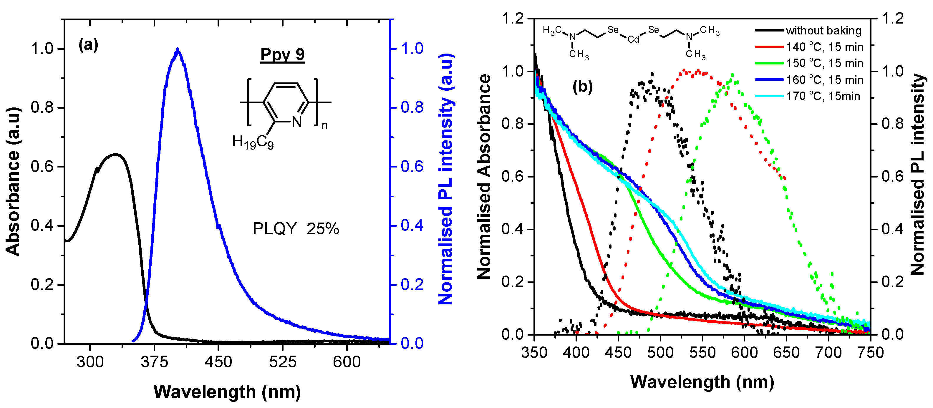
Abstract
:1. Introduction
2. Materials and Methods
2.1. Materials Synthesis
2.2. Thin Film Formation and Photophysical Characterisation
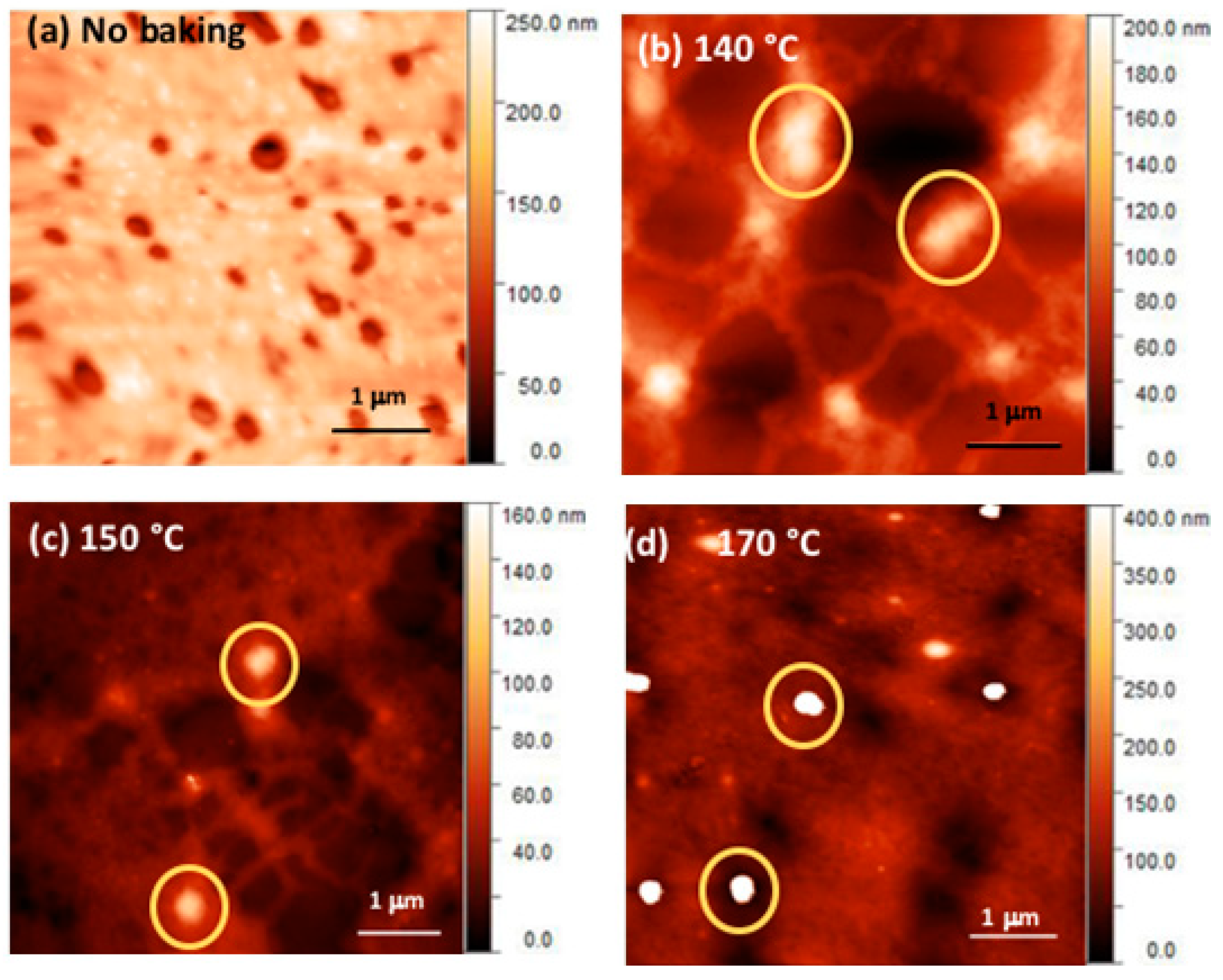
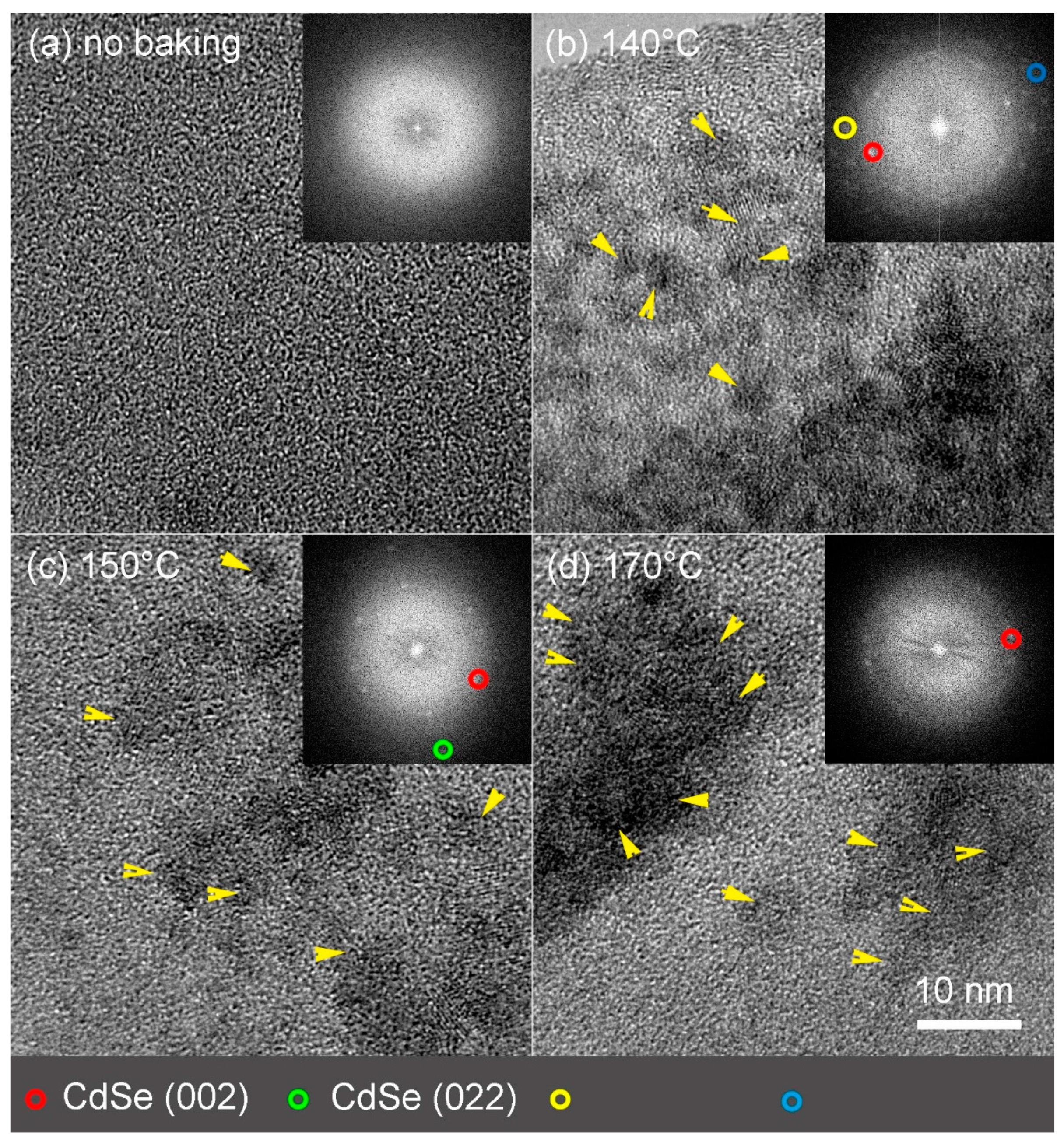
2.3. Morphological Measurements Using AFM and TEM
3. Results and Discussion
3.1. Photophysical Characterisation of Neat Films of Polymer and CdMASe Precursor
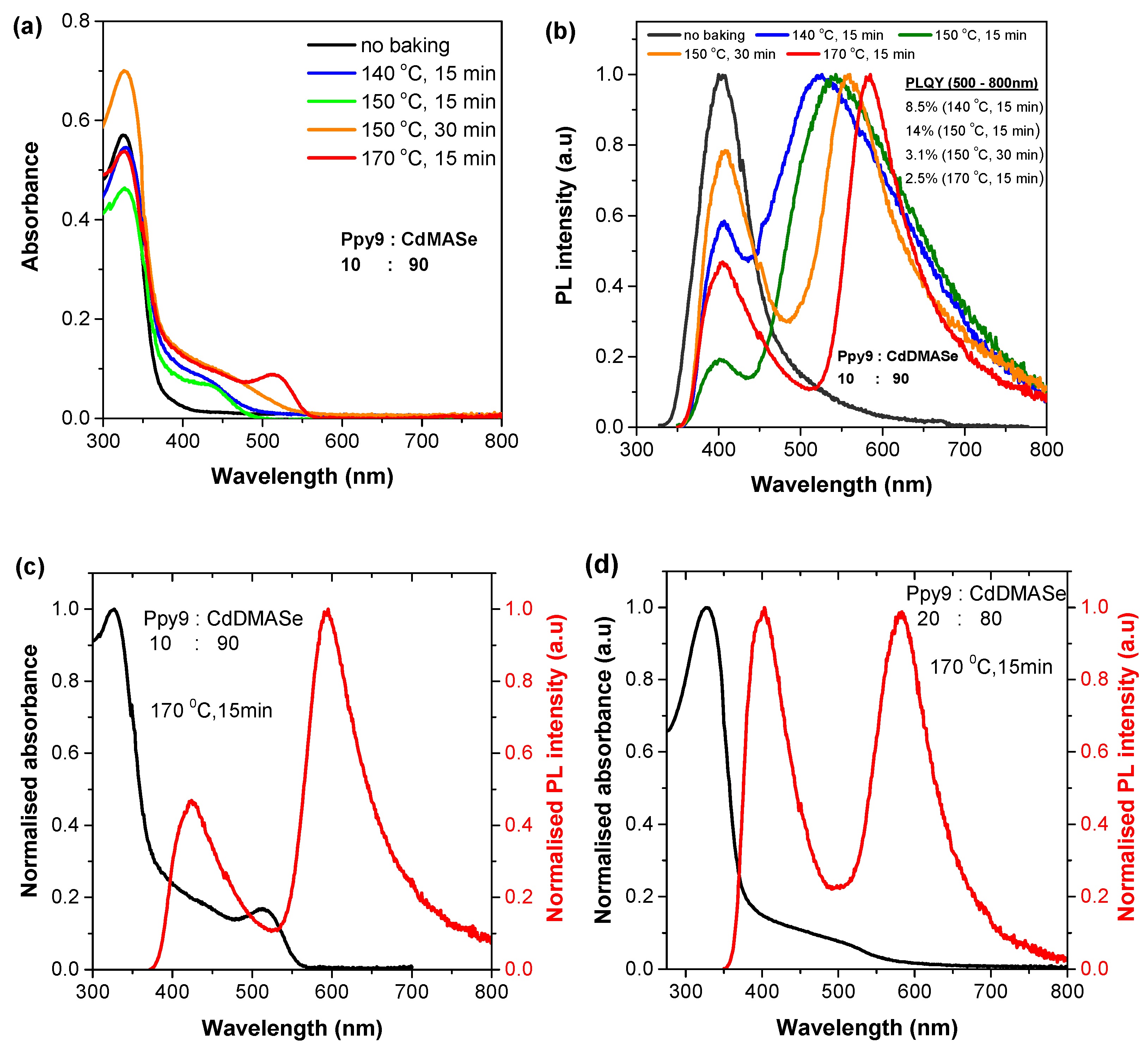
3.2. Photophysical Characterisation of Nanocomposite Polymer Films
3.3. Morphological Studies of Neat Films of Polymer and CdDMASe Precursor
4. Conclusions
Supplementary Materials
Author Contributions
Funding
Data Availability Statement
Acknowledgments
Conflicts of Interest
References
- Coe, S.; Woo, W.-K.; Bawendi, M.; Bulović, V. Electroluminescence from single monolayers of nanocrystals in molecular organic devices. Nature 2002, 420, 800–803. [Google Scholar] [CrossRef] [PubMed]
- Gudkov, S.V.; Simakin, A.V.; Bunkin, N.F.; Shafeev, G.A.; Astashev, M.E.; Glinushkin, A.P.; Grinberg, M.A.; Vodeneev, V.A. Development and application of photoconversion fluoropolymer films for greenhouses located at high or polar latitudes. J. Photochem. Photobiol. B Biol. 2020, 213, 112056. [Google Scholar] [CrossRef] [PubMed]
- Lee, H.P.; Gaharwar, A.K. Light-responsive inorganic biomaterials for biomedical applications. Adv. Sci. 2020, 7, 2000863. [Google Scholar] [CrossRef]
- Sonker, R.K.; Yadav, B.C.; Gupta, V.; Tomar, M. Synthesis of CdS nanoparticle by sol-gel method as low temperature NO2 sensor. Mater. Chem. Phys. 2020, 239, 121975. [Google Scholar] [CrossRef]
- Sajjad, M.T.; Manousiadis, P.P.; Chun, H.; Vithanage, D.A.; Rajbhandari, S.; Kanibolotsky, A.L.; Faulkner, G.; O’Brien, D.; Skabara, P.J.; Samuel, I.D.W.; et al. Novel fast color-converter for visible light communication using a blend of conjugated polymers. ACS Photonics 2015, 2, 194–199. [Google Scholar] [CrossRef] [Green Version]
- Sajjad, M.T.; Manousiadis, P.P.; Orofino, C.; Cortizo-Lacalle, D.; Kanibolotsky, A.L.; Rajbhandari, S.; Amarasinghe, D.; Chun, H.; Faulkner, G.; O’Brien, D.C.; et al. Fluorescent Red-Emitting BODIPY Oligofluorene Star-Shaped Molecules as a Color Converter Material for Visible Light Communications. Adv. Opt. Mater. 2015, 3, 536–540. [Google Scholar] [CrossRef] [Green Version]
- Jang, E.; Jun, S.; Jang, H.; Lim, J.; Kim, B.; Kim, Y. White-light-emitting diodes with quantum dot color converters for display backlights. Adv. Mater. 2010, 22, 3076–3080. [Google Scholar] [CrossRef]
- Sajjad, M.T.; Manousiadis, P.; Orofino, C.; Kanibolotsky, A.; Findlay, N.J.; Rajbhandari, S.; Vithanage, D.; Chun, H.; Faulkner, G.; O’Brien, D.C.; et al. A saturated red color converter for visible light communication using a blend of star-shaped organic semiconductors. Appl. Phys. Lett. 2017, 110, 013302. [Google Scholar] [CrossRef] [Green Version]
- Lim, J.; Jun, S.; Jang, E.; Baik, H.; Kim, H.; Cho, J. Preparation of highly luminescent nanocrystals and their application to light-emitting diodes. Adv. Mater. 2007, 19, 1927–1932. [Google Scholar] [CrossRef]
- Luo, Z.; Xu, D.; Wu, S.-T. Emerging quantum-dots-enhanced LCDs. J. Disp. Technol. 2014, 10, 526–539. [Google Scholar] [CrossRef]
- Zhu, R.; Luo, Z.; Chen, H.; Dong, Y.; Wu, S.-T. Realizing Rec. 2020 color gamut with quantum dot displays. Opt. Express 2015, 23, 23680–23693. [Google Scholar] [CrossRef] [Green Version]
- Hu, Z.; Yin, Y.; Ali, M.U.; Peng, W.; Zhang, S.; Li, D.; Zou, T.; Li, Y.; Jiao, S.; Chen, S.-j.; et al. Inkjet printed uniform quantum dots as color conversion layers for full-color OLED displays. Nanoscale 2020, 12, 2103–2110. [Google Scholar] [CrossRef] [PubMed]
- Steckel, J.S.; Ho, J.; Hamilton, C.; Xi, J.; Breen, C.; Liu, W.; Allen, P.; Coe-Sullivan, S. Quantum dots: The ultimate down-conversion material for LCD displays. J. SID 2015, 23, 294–305. [Google Scholar] [CrossRef]
- Shu, Y.; Lin, X.; Qin, H.; Hu, Z.; Jin, Y.; Peng, X. Quantum Dots for Display Applications. Angew. Chem. Int. Ed. 2020, 59, 22312–22323. [Google Scholar] [CrossRef] [PubMed]
- Ko, Y.-H.; Prabhakaran, P.; Choi, S.; Kim, G.-J.; Lee, C.; Lee, K.-S. Environmentally friendly quantum-dot color filters for ultra-high-definition liquid crystal displays. Sci. Rep. 2020, 10, 15817. [Google Scholar] [CrossRef] [PubMed]
- Wang, J.; Wang, C.-F.; Shen, H.-X.; Chen, S. Quantum-dot-embedded ionomer-derived films with ordered honeycomb structures via breath figures. Chem. Commun. 2010, 46, 7376–7378. [Google Scholar] [CrossRef]
- Harwell, J.; Burch, J.; Fikouras, A.; Gather, M.C.; Di Falco, A.; Samuel, I.D.W. Patterning multicolor hybrid perovskite films via top-down lithography. ACS Nano 2019, 13, 3823–3829. [Google Scholar] [CrossRef] [PubMed] [Green Version]
- Bansal, A.K.; Antolini, F.; Sajjad, M.T.; Stroea, L.; Mazzaro, R.; Ramkumar, S.; Kass, K.-J.; Allard, S.; Scherf, U.; Samuel, I.W. Photophysical and structural characterisation of in situ formed quantum dots. Phys. Chem. Chem. Phys. 2014, 16, 9556–9564. [Google Scholar] [CrossRef] [Green Version]
- Bansal, A.K.; Sajjad, M.T.; Antolini, F.; Stroea, L.; Gečys, P.; Raciukaitis, G.; André, P.; Hirzer, A.; Schmidt, V.; Ortolani, L.; et al. In situ formation and photo patterning of emissive quantum dots in small organic molecules. Nanoscale 2015, 7, 11163–11172. [Google Scholar] [CrossRef] [Green Version]
- Lee, J.; Sundar, V.C.; Heine, J.R.; Bawendi, M.G.; Jensen, K.F. Full color emission from II–VI semiconductor quantum dot–polymer composites. Adv. Mater. 2000, 12, 1102–1105. [Google Scholar] [CrossRef]
- Smith, A.M.; Nie, S. Semiconductor nanocrystals: Structure, properties, and band gap engineering. Acc. Chem. Res. 2010, 43, 190–200. [Google Scholar] [CrossRef] [Green Version]
- Antolini, F.; Orazi, L. Quantum dots synthesis through direct laser patterning: A review. Front. Chem. 2019, 7, 252. [Google Scholar] [CrossRef]
- Antolini, F.; Burresi, E.; Stroea, L.; Morandi, V.; Ortolani, L.; Accorsi, G.; Blosi, M. Time and temperature dependence of CdS nanoparticles grown in a polystyrene matrix. J. Nanomater. 2012, 2012, 1–11. [Google Scholar] [CrossRef]
- Kedarnath, G.; Dey, S.; Jain, V.K.; Dey, G.K.; Varghese, B. 2-(N, N-Dimethylamino) ethylselenolates of cadmium (II): Syntheses, structure of [Cd3 (OAc) 2 (SeCH2CH2NMe2) 4] and their use as single source precursors for the preparation of CdSe nanoparticles. Polyhedron 2006, 25, 2383–2391. [Google Scholar] [CrossRef]
- Yamamoto, T. Electrically conducting and thermally stable π-conjugated poly (arylene) s prepared by organometallic processes. Prog. Polym. Sci. 1992, 17, 1153–1205. [Google Scholar] [CrossRef]
- Maruyama, T.; Kubota, K.; Yamamoto, T. .pi.-Conjugated soluble poly (6-hexylpyridine-2, 5-diyl) and poly (6, 6′-dihexyl-2, 2′-bipyridine-5, 5′-diyl) with high molecular weights and n-type conducting properties. Synthesis, electrical and optical properties, and chemical reactivities of the polymers. Macromolecules 1993, 26, 4055–4057. [Google Scholar]
- Zhitomirsky, D.; Kramer, I.J.; Labelle, A.J.; Fischer, A.; Debnath, R.; Pan, J.; Bakr, O.M.; Sargent, E.H. Colloidal quantum dot photovoltaics: The effect of polydispersity. Nano Lett. 2012, 12, 1007–1012. [Google Scholar] [CrossRef]
- Shirasaki, Y.; Supran, G.J.; Bawendi, M.G.; Bulović, V. Emergence of colloidal quantum-dot light-emitting technologies. Nat. Photonics 2013, 7, 13–23. [Google Scholar] [CrossRef]
- Chan, Y.-H.; Ye, F.; Gallina, M.E.; Zhang, X.; Jin, Y.; Wu, I.-C.; Chiu, D.T. Hybrid semiconducting polymer dot–quantum dot with narrow-band emission, near-infrared fluorescence, and high brightness. J. Am. Chem. Soc. 2012, 134, 7309–7312. [Google Scholar] [CrossRef] [PubMed] [Green Version]
- Yuan, X.; Zhao, J.; Jing, P.; Zhang, W.; Li, H.; Zhang, L.; Zhong, X.; Masumoto, Y. Size-and composition-dependent energy transfer from charge transporting materials to ZnCuInS quantum dots. J. Phys. Chem. C 2012, 116, 11973–11979. [Google Scholar] [CrossRef]
- Zhong, H.; Bai, Z.; Zou, B. Tuning the luminescence properties of colloidal I–III–VI semiconductor nanocrystals for optoelectronics and biotechnology applications. J. Phys. Chem. Lett. 2012, 3, 3167–3175. [Google Scholar] [CrossRef] [PubMed]
- Talapin, D.V.; Lee, J.-S.; Kovalenko, M.V.; Shevchenko, E.V. Prospects of colloidal nanocrystals for electronic and optoelectronic applications. Chem. Rev. 2010, 110, 389–458. [Google Scholar] [CrossRef] [PubMed]
- Singh, V.; More, P.V.; Hemmer, E.; Mishra, Y.K.; Khanna, P.K. Magic-sized CdSe nanoclusters: A review on synthesis, properties and white light potential. Mater. Adv. 2021, 2, 1204–1228. [Google Scholar] [CrossRef]


Publisher’s Note: MDPI stays neutral with regard to jurisdictional claims in published maps and institutional affiliations. |
© 2021 by the authors. Licensee MDPI, Basel, Switzerland. This article is an open access article distributed under the terms and conditions of the Creative Commons Attribution (CC BY) license (https://creativecommons.org/licenses/by/4.0/).
Share and Cite
Sajjad, M.T.; Bansal, A.K.; Antolini, F.; Preis, E.; Stroea, L.; Toffanin, S.; Muccini, M.; Ortolani, L.; Migliori, A.; Allard, S.; et al. Development of Quantum Dot (QD) Based Color Converters for Multicolor Display. Nanomaterials 2021, 11, 1089. https://doi.org/10.3390/nano11051089
Sajjad MT, Bansal AK, Antolini F, Preis E, Stroea L, Toffanin S, Muccini M, Ortolani L, Migliori A, Allard S, et al. Development of Quantum Dot (QD) Based Color Converters for Multicolor Display. Nanomaterials. 2021; 11(5):1089. https://doi.org/10.3390/nano11051089
Chicago/Turabian StyleSajjad, Muhammad T., Ashu K. Bansal, Francesco Antolini, Eduard Preis, Lenuta Stroea, Stefano Toffanin, Michele Muccini, Luca Ortolani, Andrea Migliori, Sybille Allard, and et al. 2021. "Development of Quantum Dot (QD) Based Color Converters for Multicolor Display" Nanomaterials 11, no. 5: 1089. https://doi.org/10.3390/nano11051089