Abstract
CsPbIBr2, a cesium-based all-inorganic halide perovskite (CsPe), is a very promising alternative material to mainstream organic–inorganic hybrid halide perovskite (HPe) materials owing to its exceptional moisture stability, thermal stability, and light stability. However, because of the wide band gap (2.05 eV) of CsPbIBr2, it has a low power conversion efficiency (PCE), which hinders its application in highly efficient solar cells. In this study, a facile nanoimprinted one-dimensional grating nanopattern (1D GNP) formation on mesoporous TiO2 (mp-TiO2) photoelectrodes was introduced to improve the effective light utilization and enhance the performance of CsPbIBr2 perovskite solar cells (PSCs). The 1D GNP structure on the mp-TiO2 layer increases the light absorption efficiency by diffracting the unabsorbed light into the active mp-TiO2 and CsPbIBr2 layers as well as increasing the charge separation and collection due to the extended interfacial contact area between the mp-TiO2 and CsPbIBr2 layers. Consequently, both the current density (JSC) and the fill factor (FF) of the fabricated cells improved, leading to over a 20% enhancement in the solar cell’s PCE. Thus, this periodic grating structure, fabricated by simple nanoimprinting, could play an important role in the large-scale production of highly efficient and cost-effective Cs-based PSCs.
1. Introduction
The power conversion efficiency (PCE) of organic–inorganic hybrid halide perovskite (HPe) solar cells has improved dramatically over the last ten years, rising from 3.81% in 2009 to 25.5% in 2021 [1,2]. This remarkable progress is mainly attributed to the outstanding properties of HPe cells, which include strong light absorption in the visible region, high charge carrier mobility, and long charge diffusion length [1,3]. HPe has a typical ABX3 structure, where A is an organic cation (mainly CH3NH3+ (MA+) and/or NH2CHNH2+ (FA+)), B is an inorganic cation (Pb2+, Ge2+, Sn2+), and X is a halogen anion (I−, Br−, Cl−). Although HPe cells can achieve a very high PCE, their thermal, light, and moisture stabilities are not sufficient for device commercialization because of the intrinsically volatile and hygroscopic properties of organic cation moieties, such as MA+ or FA+ [4].
To overcome the limitations of HPe, several methods have been developed, including metal doping in the perovskite phase [5], interface/surface treatment [6], device encapsulation [7], and employing an all-inorganic perovskite composition [8,9,10]. Among these methods, the most used strategy is to replace the volatile organic group with non-volatile inorganic cesium (Cs) cations to make a Cs-based all-inorganic perovskite (CsPe) light absorption layer. For example, CsPe-based (CsPbX3, where X = I, Br, Cl, or their mixture) perovskite solar cells (PSCs) have shown remarkable stability under 80% humidity or 100 °C heating conditions [11,12]. The efficiency of CsPbX3 is closely related to its halide composition, which leads to a change in its crystal structure, band gap, and humidity tolerance. The currently studied inorganic perovskite compositions are mainly CsPbI3, CsPbI2Br, CsPbIBr2, and CsPbBr3, based on the type of halide and its ratio. Among these all-inorganic Cs-based perovskites, α-phase CsPbI3 is the most widely investigated perovskite owing to its narrow band gap (Eg = 1.73 eV), suitability for absorbing visible light, and excellent efficiency of 17.06%. However, black α-phase CsPbI3 suffers from severe instability and easily degrades to a non-perovskite yellow δ-phase CsPbI3 (Eg = 2.82 eV), even at room temperature. These are the major issues that delimit the fabrication of solar cell devices using CsPbI3 [13,14]. On the other hand, the CsPbBr3 PSCs, all containing bromide CsPe, have shown exceptional stability, even without any passivation. However, a CsPbBr3 layer has a very narrow light absorption range of only up to 540 nm owing to its wide band gap (Eg = 2.3 eV), which results in a lower PCE [15]. Therefore, exchanging some iodide ions with bromide ions in CsPe to form a mixed-halide CsPe (CsPbI3−xBrx) could be a good alternative for improving the phase stability. CsPbI2Br, a mixed-halide CsPe, has a slightly narrow band gap of 1.92 eV and shows better stability than CsPbI3 does; however, for CsPbI2Br, overcoming the stability issue is still a challenge [16,17]. Finally, CsPbIBr2 (another mixed-halide CsPe) has been considered as the best candidate among all the possible Cs-based inorganic perovskites because it has an acceptable band gap of 2.05 eV and possesses a superior phase stability in air. Moreover, CsPbIBr2 has a typical bright red color that is suitable for applications in tandem devices and colorful smart photovoltaic windows [18,19]. Over the years, the PCE of CsPbIBr2 has been improved from 4.7% to the recent highest efficiency of 10.88% by introducing various strategies, such as the optimization of the fabrication process to obtain a better film quality, interface/surface engineering, and elemental impurity doping for energy-level control and good charge carrier transport [19,20,21,22,23]. Although the cell performance of CsPbIBr2 is significantly improved by these effective modifications, its PCE is still constrained compared to that of the organic–inorganic hybrid PSCs. This limited PCE is caused by a poor light absorption wavelength edge of 600 nm due to its intrinsic wide band gap. To address this limited light absorption characteristic, several photon management techniques, such as utilization of the surface plasmonic effect, anti-reflection schemes, and periodic gratings, have been applied and studied to increase the time of residence of the targeted photons in the photoactive layer [24,25,26,27,28]. Considering the results of these previous studies, we can conclude that a promising approach to improve the light absorption of a wide band gap CsPbIBr2 (without increasing its thickness) is to diffract the incident light and maximize the light dwelling time in the CsPbIBr2 layer by employing a periodic grating.
In this study, we introduced a one-dimensional grating nanopattern (1D GNP) over a mesoporous TiO2 (mp-TiO2) layer using solvent-assisted nanoimprinting and applied it to CsPbIBr2 PSCs to increase their light harvesting as well as their charge collection. As a result, the device with a flat mp-TiO2 layer exhibited a PCE of 3.5%, while the device with a 1D GNP mp-TiO2 layer achieved a PCE of 4.3%, which is an ~23% improvement in the PCE due to the increase in the photogenerated current density (JSC) and fill factor (FF) of the CsPbIBr2 PSCs. In addition, this periodic nano-grating process can be applicable for mass production at a low cost, as it allows high reproducibility with reusable masks and molds.
2. Materials and Methods
2.1. Materials Used and Nanopatterned PDMS Mold Preparation
CsI (99.9%), PbBr2 (99.999%), dimethyl sulfoxide (DMSO, anhydrous, >99.9%), chlorobenzene (CB, anhydrous, 99.8%), and 1H,1H,2H,2H-Perfluorooctyl-trichlorosilane (PFOTCS, 97%) were purchased from Sigma-Aldrich (St. Louis, MO, USA). TiO2 solutions, SC-BT060 and SC-HT040 (anatase structure, particle size 50 nm), were purchased from Sharechem Co. (Hwaseong, South Korea) to fabricate the compact TiO2 (c-TiO2) layer and the mp-TiO2 layer, respectively. Poly[[4,8-bis[(2-ethylhexyl)oxy]benzo[1,2-b:4,5-b’]dithiophene-2,6-diyl][3-fluoro-2-[(2-ethylhexyl)carbonyl]thieno[3,4-b]thiophenediyl]] (PTB7, average molecular weight of 116 kDa, polydispersity index of 2.5) was purchased from 1-Material Inc (Dorval, QC, Canada). All chemicals were used in the form as delivered by the manufacturer without further purification.
To prepare a 1D GNP prepatterned polydimethylsiloxane (PDMS) mold, the silicon (Si) master (grating period of 605 nm, grating depth of 190 nm; LightSmyth Technologies Inc. (Eugene, OR, USA)) was set on a thin plate. A few drops of PFOTCS near the Si master were used to make the Si master surface hydrophobic to facilitate easy removal of the Si master from the PDMS mold. Next, the PDMS pre-polymer was obtained by mixing a Sylgard 184 elastomer kit (with a 10:1 weight ratio of elastomer base to curing agent, Dow Corning (Midland, MI, USA)) for 30 min and letting it degas for 1 h in a vacuum oven. Then, the PDMS pre-polymer was poured onto the Si master and cured at 100 °C for 40 min. The cured PDMS mold was detached from the Si master and used for the nanopatterning of the mp-TiO2 layer.
2.2. Device Fabrication
We fabricated CsPbIBr2 solar cells with an FTO/c-TiO2 (30 nm)/mp-TiO2 (330 nm)/CsPbIBr2 (300 nm)/PTB7 (40 nm)/Au (70 nm) structure, where PTB7 was used as a hole transport layer (HTL) (see Figure 1a). After cleaning the FTO substrate, a 30-nanometer c-TiO2 layer was spin-coated using an SC-BT060 solution at 3000 rpm for 30 s and annealed at 500 °C for 30 min. Then, to deposit the flat mp-TiO2 layer, the SC-HT040 paste was spin-coated and annealed on the bl-TiO2/FTO substrate at 3000 rpm for 30 s and at 500 °C for 30 min, respectively. For the 1D GNP mp-TiO2 layer, the PDMS mold was immediately placed onto the spin-coated mp-TiO2 paste with appropriate pressure to apply a nanoimprinting process before the paste surface dried. After complete surface contact between the PDMS mold and the mp-TiO2 paste, a heat treatment at 125 °C for 5 min was performed to remove the residual solvent. Next, the nanopatterned mp-TiO2 was separated from the PDMS mold and annealed at 500 °C for 30 min (see Figure 1b).
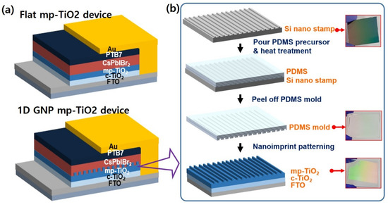
Figure 1.
Schematics of (a) the device structure of CsPbIBr2 solar cells with flat mp-TiO2 and 1D GNP mp-TiO2, and (b) the fabrication process for 1D GNP mp-TiO2.
To prepare the CsPbIBr2 layer, a precursor solution (1 M solution of CsI and PbBr2 in DMSO) was spin-coated on the flat or 1D GNP mp-TiO2 layer at 2500 rpm for 60 s and heated at 160 °C for 20 min. Subsequently, PTB7 solution (5 mg/1 mL CB) was spin-coated on the CsPbIBr2 layer at 3000 rpm for 60 s and dried on a hot plate at 70 °C for 30 min in air. Finally, a 70-nanometer Au layer was deposited to make counter electrodes using a thermal evaporator under a high vacuum pressure of 5.0 × 10⁻⁶ Torr. The active area of the fabricated devices was 0.16 cm2.
2.3. Characterization and Analysis
The cross-sectional and top-view images of the mp-TiO2 layer were obtained using field emission scanning electron microscopy (FE-SEM, S-4800, Hitachi, Tokyo, Japan). The transmission, reflection, and absorption properties of mp-TiO2 were characterized using UV–Vis spectrometry (Lambda 750, Perkin Elmer, Waltham, MA, USA). A multi-purpose X-ray diffraction (XRD) system (Empyrean, PANalytical, Almelo, The Netherlands) was used to determine the structure of the CsPbIBr2 perovskite layer. The current density–voltage (J–V) characteristics under light and dark conditions were measured using a solar cell measurement system equipped with a Keithley-2400 source measure unit and a solar simulator (91192, Newport, Irvine, CA, USA). The light intensity of the illumination was set to AM1.5G (100 mW/cm2) and monitored using a radiant power meter (70260, Oriel). The external quantum efficiency (EQE) spectrum was measured using a QuantX-300 system (Newport). The series resistance (RS) and shunt resistance (RSH) of the devices were extracted from the slope of the light J–V curves near the open-circuit voltage (VOC) and JSC regions, respectively.
To investigate the optical absorption in the CsPbIBr2 active layer, the solar cells were analyzed using the three-dimensional (3D) finite difference time-domain (FDTD) method (FDTD Solution, Lumerical Inc., Vancouver, BC, Canada). In the optical simulation, the solar cells were composed of glass/FTO/c-TiO2/mp-TiO2 (flat and 1D GNP)/CsPbIBr2/PTB7/Au. A plane wave with a wavelength range of 300 to 700 nm was used as an incident light source. A frequency-domain field and power monitor was set up to evaluate the total absorbed power and the spatial profile of the optical absorption per unit volume of the CsPbIBr2 active layer.
3. Results and Discussion
The mp-TiO2 with a 1D GNP structure exhibits a rainbow-colored visual effect due to the optical interference caused by the grating nanopattern (see the bottom inset of Figure 1b).
Figure 2a,b show the SEM images of the mp-TiO2 layer, with and without a 1D GNP structure, respectively. The cross-sectional and top-view images of the 1D GNP mp-TiO2 show a clear periodic pattern over the entire large area without fragments or cracks. The period, width, and height of the 1D GNP mp-TiO2 are about 610, 250, and 100 nm, respectively. XRD measurements were performed to reveal the formation of the CsPbIBr2 perovskite layer (Figure 2c). The typical diffraction peaks in the XRD patterns were matched to α-phase CsPbIBr2 and were found to be consistent with those in previous reports. The three dominant diffraction peaks at 15.02°, 21.27°, and 30.15° that are indexed to the (100), (110), and (200) planes, respectively, show good crystallinity and morphology of the CsPbIBr2 perovskite layer, which are further confirmed by the SEM image in the inset of Figure 2c [20,29,30,31]. We can also see the XRD peak at 25.2° from the (101) plane of the anatase TiO2 structure, as we used a TiO2 nanoparticle solution (crystal structure: anatase; average size: 50 nm) to fabricate an mp-TiO2 layer. The anatase TiO2 has been generally accepted as an electron transport layer of solar cells because of its low cost, transparency, and higher conduction band level for a fast electron transport and high VOC [32,33].
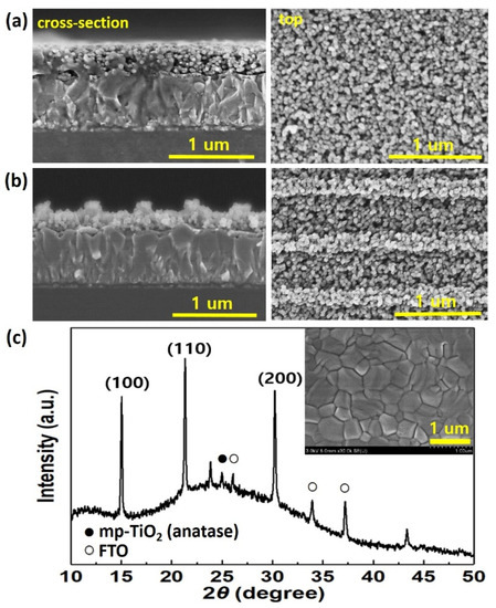
Figure 2.
(a) Cross-section and top-view SEM images of the flat mp-TiO2 and (b) the 1D GNP mp-TiO2. (c) XRD data for the CsPbIBr2 layer (the inset shows the surface morphology of the CsPbIBr2 layer). The solid circle and open circle denote the peaks from the mp-TiO2 (anatase) and FTO substrates, respectively.
Figure 3a and Table 1 represent the light J–V properties for the solar cells with and without a 1D GNP pattern under AM 1.5G (100 mW/cm2). The efficiency of the CsPbIBr2 solar cell was improved by the introduction of a 1D GNP onto the mp-TiO2 layer. The flat mp-TiO2 device exhibited a VOC of 0.971 V, a JSC of 7.98 mA/cm2, an FF of 45.17%, and a PCE of 3.5%. However, in the 1D GNP mp-TiO2 device, all these parameters increased. The VOC, JSC, and FF increased to 0.975 V, 8.88 mA/cm2, and 49.73%, respectively, leading to a PCE of 4.31%. The introduction of a 1D GNP pattern resulted in a PCE enhancement of ~23%, primarily due to the improvement in the JSC. (Here, we note that although there is a large difference in the PCE compared with the recently reported best efficiency of 10.88% [18,22], our device efficiency of ca. 4% is reasonable because the devices were made via a very basic one-step coating process without using any improved methods, such as anti-solvent dropping, interface treatment, impurity doping, etc.)
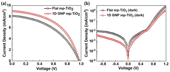
Figure 3.
Current density–voltage (J–V) properties of CsPbIBr2 solar cells with a flat mp-TiO2 and a 1D GNP mp-TiO2 under (a) one sun illumination and (b) dark conditions.

Table 1.
Summary of device performance with a flat mp-TiO2 and a 1D GNP mp-TiO2 under AM 1.5 G conditions.
To understand the working principle for these improvements, we further investigated the optical and electrical properties of the devices. First, the reflectance, transmittance, and absorbance of the glass/FTO/c-TiO2/mp-TiO2 samples were measured using a UV–Vis spectrometer to study the optical effect of a 1D GNP on the mp-TiO2, where the beam was incident on the glass side. The measured reflectance of the mp-TiO2 with a 1D GNP (average ≈13.8%) was higher than that of the flat mp-TiO2 (average ≈12.3%), as shown in Figure 4a. In contrast, the transmittance of the mp-TiO2 with a 1D GNP (average ≈ 62.2%) was lower than that of the flat mp-TiO2 (average ≈ 69.1%). Therefore, the 1D GNP mp-TiO2 can absorb more light than the flat one over a broad range of wavelengths (see Figure 4b,c) [34,35]. This is attributed to the increased optical path length and light trapping effect that diffracts the unabsorbed light back into the mp-TiO2 photoelectrode at an oblique angle, which can further result in enhanced photon absorption in the CsPbIBr2 active layer, as depicted in the FDTD simulation results.
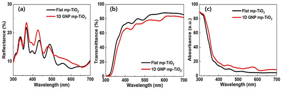
Figure 4.
(a) Reflectance, (b) transmittance, and (c) absorbance spectra of the flat mp-TiO2 and the 1D GNP mp-TiO2 layers.
Compared to the flat mp-TiO2, we can see the obvious light diffraction effect of the 1D GNP mp-TiO2 from the corresponding digital camera images in Figure 5.
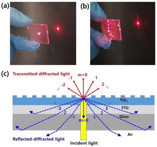
Figure 5.
Digital camera images of the diffracted light from (a) a flat mp-TiO2 and (b) a 1D GNP mp-TiO2. (c) Schematic illustration of grating diffraction.
As illustrated in Figure 5c, the incident light is diffracted into multiple orders of transmitted and reflected light (m = …, −2, –1, 0, 1, 2, …) toward different directions at the grating interface [36]. Figure 5a,b show the light diffracted and reflected by the flat mp-TiO2 and the 1D GNP mp-TiO2, respectively, using a He–Ne laser (632.8 nm). In Figure 5a,b, we can observe the reflected light on the glass surface and the diffracted light on the front black screen in the case of the 1D GNP mp-TiO2, whereas the flat mp-TiO2 shows only a strong transmitted light without the diffracted and reflected light. Additionally, the zeroth-order transmitted light of the 1D GNP mp-TiO2 is weaker than that of the flat mp-TiO2, which corresponds to the reflectance and transmittance spectra shown in Figure 4a,b. Furthermore, if the angle of the reflected–diffracted light is larger than the critical angle for the total internal reflection because of the slightly decreased refractive index values from the TiO2 layer to air (i.e., nTiO2 (≈2.1) > nFTO (≈1.9) > nGlass (≈1.5) > nAir (=1.0), where these refractive index values at 550 nm were estimated from previous reports [37,38]), then the light can be reflected back to the mp-TiO2 and perovskite layers, leading to an additional absorption, as illustrated in Figure 5c.
Next, we performed EQE measurements to confirm whether the current enhancement was the main factor increasing the device’s performance in the 1D GNP mp-TiO2 structure. As can be seen in Figure 6a, the EQE was improved across the entire spectral range, and the enhancement was distinguishable in the wavelength range from 330 to 570 nm. The average EQE in the measured spectral range increased by ~12.1% when accompanied by the 1D GNP structure. These EQE results indicate that a 1D GNP structure can help to reuse the diffracted light to generate more charge carriers by increasing the optical path length and light trapping.
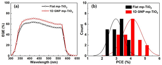
Figure 6.
(a) External quantum efficiency (EQE) spectra and (b) PCE distribution histogram of the CsPbIBr2 PSCs with and without a 1D GNP structure in the mp-TiO2 for 20 devices.
The device with the 1D GNP mp-TiO2 showed a higher FF in comparison to the control device with the flat mp-TiO2. We calculated the internal resistance of the devices (i.e., RS and RSH) from the light J–V curve and also measured the dark J–V characteristic to study the effect of a 1D GNP on device resistance. The higher FF of the 1D GNP may have been caused by the reduced interface resistance due to the increase in the contact area between the 1D GNP mp-TiO2 and the CsPbIBr2 active layer, as shown in the dark J–V curves in Figure 3b. The decreased RS and increased RSH indicate a better charge transport that could be another factor causing the observed high FF in the devices with a 1D GNP mp-TiO2 [37,39].
To compare the performance enhancement exhibited by the 1D nanostructures, we fabricated and measured 20 perovskite solar cells, with and without the 1D GNP mp-TiO2 layer. Figure 6b shows the histograms of PCE distributions for each type of solar cell. We can observe a consistent and reproducible PCE improvement trend in the case of the 1D GNP mp-TiO2 structure.
Finally, we performed numerical simulations using the FDTD method to investigate the effects of the diffraction grating in the fabricated solar cell. Figure 7 shows the optical characteristics of the total device structure illustrated in Figure 1, especially for absorbed power. The spectral response of the average absorbed power in the CsPbIBr2 layer with a flat and a 1D GNP mp-TiO2 is shown in Figure 7a. Considering the total spectral absorbed power, the device with the 1D GNP mp-TiO2 layer showed higher absorption in the active layer than that of the device with the flat mp-TiO2 layer. Although this enhancement factor is not exactly the same as that of the EQE results, the spectral trend corresponds with the spectral trend of the EQE of fabricated solar cells in Figure 6a. In the case of the absorbed power, the increase was distinguishable in the wavelength range from 330 to 560 nm. The average value of the absorbed power in the wavelength range from 300 to 650 nm was 0.760 in the 1D GNP structured device. This represents an increase of 17.1% compared to the flat device, which had a value of 0.649 for the average spectral absorbed power.
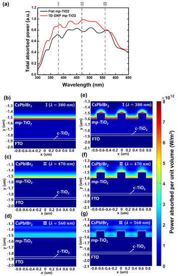
Figure 7.
Calculated results of the solar cells with flat and 1D GNP mp-TiO2 layers. (a) Spectral response of total absorbed power in the CsPbIBr2 active layer. (b–g) Spatial profiles of power absorbed per unit volume with respect to the xy-plane at the three different wavelengths (380, 470, and 560 nm): (b–d) case of the flat mp-TiO2 layer; (e–g) case of the 1D GNP mp-TiO2 layer.
The spatial profiles of power absorbed per unit volume with respect to the xy-plane of the solar cells with a flat and a 1D GNP mp-TiO2 were analyzed to further evaluate the diffraction effects in a CsPbIBr2 layer. Figure 7b–d show the light absorption profiles of the flat mp-TiO2 device and Figure 7e–g show those of the 1D GNP mp-TiO2 structure at wavelengths of 380, 470, and 560 nm, respectively. The optical absorption for the solar cells with a flat mp-TiO2 layer occurs strongly at the interface between the mp-TiO2 layer and the CsPbIBr2 layer. Compared to the flat mp-TiO2, the amount of absorption in the CsPbIBr2 layer with a 1D GNP mp-TiO2 increased at the interface between the mp-TiO2 layer and the CsPbIBr2 layer by the diffraction grating effects at wavelengths of 380 and 470 nm, respectively. At the wavelength of 560 nm, the value of the total absorbed power at point III in Figure 7a appears almost the same because the absorbed power of the absorbing layer is similar to that in the spatial profile in Figure 7d,g.
It shows that the light is trapped inside the active layer by the increased optical path length and the total internal reflection when the light is diffracted at a specific wavelength. In addition, the diffracted light within an absorption layer improves the light harvesting at the interface between the mp-TiO2 layer and the CsPbIBr2 layer [27,28]. The fabricated 1D GNP mp-TiO2 layer was not completely square shaped, as shown in Figure 2b. In addition, the measured refractive index values were applied to the mp-TiO2 grating structure without porous media. The amount of absorption in the active layer was not exactly matched with the enhanced factor of the EQE in the experimental results owing to these imperfections. However, the overall trends correspond with each other, and it can be inferred that the diffraction grating enhances the absorption inside the active layer and consequently improves the power conversion efficiency of the solar cells. Moreover, because the grating pattern is formed with periodicity, it is advantageous for mass production compared to other nano patterns. For example, laser interference lithography contains the exposure process with the interference of a light source that can be formed by two-beam interference; thus, it does not require any masking components. The nanoimprinting technology used in this work shows high reproducibility with reusable masks [40,41].
4. Conclusions
We successfully introduced a 1D GNP structure onto mp-TiO2 and fabricated a high-performance CsPbIBr2 perovskite solar cell using a simple nanoimprinting method with a PDMS mold. It is evident from the UV–Vis spectra, EQE measurement data, and FDTD simulation data that the 1D GNP structure can diffract the incident light to increase the optical path length within the mp-TiO2 and active layers, thus leading to an enhancement in the light harvest of the devices over a broad wavelength range. In addition, the 1D GNP structure increases the FF by improving the electron extraction and suppressing the charge recombination due to the increased interfacial contact area between the mp-TiO2 and CsPbIBr2 layers, where excitons are separated and charge transfer occurs. As a result, the PSCs with the 1D GNP mp-TiO2 achieved a PCE of 4.31%, which is almost 23% higher than that of the flat mp-TiO2 PSCs (3.5%).
We believe that nanoimprinting a 1D GNP structure onto an mp-TiO2 photoelectrode, which optimizes light harvesting, can be an effective way to improve the photoelectric properties of various Cs-based perovskite applications, including solar cells, photodetectors, light-emitting diodes, and solar water-splitting devices.
Author Contributions
K.-P.K. and S.W. executed idea conceptualization and experimental design; K.-P.K., S.M.K., and W.H.K. performed the experiments and characterization; J.Y.K. and Y.S.D. performed the FDTD analysis; K.-P.K., S.M.K. and S.W. performed the main data analysis; S.W. and Y.S.D. wrote the draft manuscript. All authors have read and agreed to the published version of the manuscript.
Funding
This research received no external funding.
Institutional Review Board Statement
Not applicable.
Informed Consent Statement
Not applicable.
Data Availability Statement
Not applicable.
Acknowledgments
This study was supported by the DGIST R&D Program of the Ministry of Science and ICT of Korea (20-ET-08) and the National Research Foundation of Korea (NRF) grant funded by the Korea government (MSIT) (NRF-2019R1C1C1007569).
Conflicts of Interest
The authors declare no conflict of interest.
References
- Park, N.K. Research direction toward scalable, stable, and high efficiency perovskite solar cells. Adv. Energy Mater. 2020, 10, 1903106. [Google Scholar] [CrossRef]
- Best Research-Cell Efficiency Chart. Available online: https://www.nrel.gov/pv/cell-efficiency.html (accessed on 4 January 2021).
- Huang, J.; Yuan, Y.; Shao, Y.; Yan, Y. Understanding the physical properties of hybrid perovskites for photovoltaic applications. Nat. Rev. Mater. 2017, 2, 17042. [Google Scholar] [CrossRef]
- Wang, R.; Mujahid, M.; Duan, Y.; Wang, Z.K.; Xue, J.; Yang, Y. A Review of Perovskites Solar Cell Stability. Adv. Funct. Mater. 2019, 29, 1808843. [Google Scholar] [CrossRef]
- Chan, S.H.; Wu, M.C.; Lee, K.M.; Chen, W.C.; Lin, T.H.; Su, W.F. Enhancing perovskite solar cell performance and stability by doping barium in methylammonium lead halide. J. Mater. Chem. A 2017, 5, 18044–18052. [Google Scholar] [CrossRef]
- Chen, J.; Park, N.G. Materials and methods for interface engineering toward stable and efficient perovskite solar cells. ACS Energy Lett. 2020, 5, 2742–2786. [Google Scholar] [CrossRef]
- Cheacharoen, R.; Rolston, N.; Harwood, D.; Bush, K.A.; Dauskardt, R.H.; McGehee, M.D. Design and understanding of encapsulated perovskite solar cells to withstand temperature cycling. Energy Environ. Sci. 2018, 11, 144–150. [Google Scholar] [CrossRef]
- Duan, J.; Xu, H.; Sha, W.E.I.; Zhao, Y.; Wang, Y.; Yang, X.; Tang, Q. Inorganic perovskite solar cells: An emerging member of the photovoltaic community. J. Mater. Chem. A 2019, 7, 21036–21068. [Google Scholar] [CrossRef]
- Ouedraogo, N.A.N.; Chen, Y.; Xiao, Y.Y.; Meng, Q.; Han, C.B.; Yan, H.; Zhang, Y. Stability of all inorganic perovskite solar cells. Nano Energy 2020, 67, 104249. [Google Scholar] [CrossRef]
- Xiang, W.; Tress, W. Review on recent progress of all-inorganic metal halide perovskites and solar cells. Adv. Mater. 2019, 31, 1902851. [Google Scholar] [CrossRef] [PubMed]
- Duan, J.; Hu, T.; Zhao, Y.; He, B.; Tang, Q. Carbon-electrode-tailored all-Inorganic perovskite solar cells to harvest solar and water-vapor energy. Angew. Chem. Int. Ed. 2018, 57, 5746–5749. [Google Scholar] [CrossRef]
- Liang, J.; Zhao, P.; Wang, C.; Wang, Y.; Hu, Y.; Zhu, G.; Ma, L.; Liu, J.; Jin, Z. CsPb0.9Sn0.1IBr2 based all-inorganic perovskite solar cells with exceptional efficiency and stability. J. Am. Chem. Soc. 2017, 139, 14009–14012. [Google Scholar] [CrossRef] [PubMed]
- Wang, Y.; Zhang, T.; Kan, M.; Zhao, Y. Bifunctional stabilization of all-inorganic alpha-CsPbI3 perovskite for 17% efficiency photovoltaics. J. Am. Chem. Soc. 2018, 140, 12345–12348. [Google Scholar] [CrossRef]
- Straus, D.B.; Guo, S.; Abeykoon, A.M.M.; Cava, R.J. Understanding the instability of the halide perovskite CsPbI3 through temperature-dependent structural analysis. Adv. Mater. 2020, 32, 2001069. [Google Scholar] [CrossRef]
- Liang, J.; Wang, C.; Wang, Y.; Xu, Z.; Lu, Z.; Ma, Y.; Zhu, H.; Hu, Y.; Xiao, C.; Yi, X.; et al. All-inorganic perovskite solar cells. J. Am. Chem. Soc. 2016, 138, 15829–15832. [Google Scholar] [CrossRef]
- Mariotti, S.; Hutter, O.S.; Phillips, L.J.; Yates, P.J.; Kundu, B.; Durose, K. Stability and performance of CsPbI2Br thin films and solar cell devices. ACS Appl. Mater. Interfaces 2018, 10, 3750–3760. [Google Scholar] [CrossRef] [PubMed]
- Zeng, Q.; Zhang, X.; Liu, C.; Feng, T.; Chen, Z.; Zhang, W.; Zheng, W.; Zhang, H.; Yang, B. Inorganic CsPbI2Br perovskite solar cells: The progress and perspective. Sol. RRL 2019, 3, 1800239. [Google Scholar] [CrossRef]
- Guo, Y.; Yin, X.; Liu, J.; Wen, S.; Wu, Y.; Que, W. Inorganic CsPbIBr2-based perovskite solar cells: Fabrication technique modification and efficiency improvement. Sol. RRL 2019, 3, 1900135. [Google Scholar] [CrossRef]
- Liu, C.; Li, W.; Chen, J.; Fan, J.; Mai, Y.; Schropp, R.E.I. Ultra-thin MoOx as cathode buffer layer for the improvement of all-inorganic CsPbIBr2 perovskite solar cells. Nano Energy 2017, 41, 75. [Google Scholar] [CrossRef]
- Zhu, W.; Zhang, Q.; Chen, D.; Zhang, Z.; Lin, Z.; Chang, J.; Zhang, J.; Zhang, C.; Hao, Y. Intermolecular exchange boosts efficiency of air-stable, carbon-based all-inorganic planar CsPbIBr2 perovskite solar cells to over 9%. Adv. Energy Mater. 2018, 8, 1802080. [Google Scholar] [CrossRef]
- Guo, Y.; Yin, X.; Liu, J.; Que, W. Highly efficient CsPbIBr2 perovskite solar cells with efficiency over 9.8% fabricated using a preheating-assisted spin-coating method. J. Mater. Chem. A 2019, 7, 19008–19016. [Google Scholar] [CrossRef]
- Subhani, W.S.; Wang, K.; Du, M.; Wang, X.; Liu, S. Interface-modification-induced gradient energy band for highly efficient CsPbIBr2 perovskite solar cells. Adv. Energy Mater. 2019, 9, 1803785. [Google Scholar] [CrossRef]
- Liang, J.; Liu, Z.; Qiu, L.; Hawash, Z.; Meng, L.; Wu, Z.; Jiang, Y.; Ono, L.K.; Qi, Y. Enhancing optical, electronic, crystalline, and morphological properties of cesium lead halide by Mn substitution for high-stability all-inorganic perovskite solar cells with carbon electrodes. Adv. Energy Mater. 2018, 8, 1800504. [Google Scholar] [CrossRef]
- Cui, J.; Chen, C.; Han, J.; Cao, K.; Zhang, W.; Shen, Y.; Wang, M. Surface plasmon resonance effect in inverted perovskite solar cells. Adv. Sci. 2016, 3, 1500312. [Google Scholar] [CrossRef]
- Tavakoli, M.M.; Tsui, K.H.; Zhang, Q.; He, J.; Yao, Y.; Li, D.; Fan, Z. Highly efficient flexible perovskite solar cells with antireflection and self-cleaning nanostructures. ACS Nano 2015, 9, 10287. [Google Scholar] [CrossRef] [PubMed]
- Luo, Q.; Deng, X.; Zhang, C.; Yu, M.; Zhou, X.; Wang, Z.; Chen, Z.; Huang, S. Enhancing photovoltaic performance of perovskite solar cells with silica nanosphere antireflection coatings. Sol. Energy 2018, 169, 128–135. [Google Scholar] [CrossRef]
- Wang, Y.; Wang, P.; Zhou, X.; Li, C.; Li, H.; Hu, X.; Li, F.; Liu, X.; Li, M.; Song, Y. Diffraction-grated perovskite induced highly efficient solar cells through nanophotonic light trapping. Adv. Energy Mater. 2018, 8, 1702960. [Google Scholar] [CrossRef]
- Deng, K.; Liu, Z.; Wang, M.; Li, L. Nanoimprinted grating-embedded perovskite solar cells with improved light management. Adv. Funct. Mater. 2019, 29, 1900830. [Google Scholar] [CrossRef]
- Subhani, W.S.; Wang, K.; Du, M.; Liu, S.F. Goldschmidt-rule-deviated perovskite CsPbIBr2 by barium substitution for efficient solar cells. Nano Energy 2019, 61, 165–172. [Google Scholar] [CrossRef]
- Yang, S.; Wang, L.; Gao, L.; Cao, J.; Han, Q.; Yu, F.; Kamata, Y.; Zhang, C.; Fan, M.; Wei, G.; et al. Excellent moisture stability and efficiency of inverted all-inorganic CsPbIBr2 perovskite solar cells through molecule interface engineering. ACS Appl. Mater. Interfaces 2020, 12, 13931–13940. [Google Scholar] [CrossRef]
- Liu, Z.; Li, H.; Qin, C.; Zhang, T.; Gu, Y.; Chen, H.; Zheng, H.; Li, S. Solution-processed inorganic perovskite flexible photodetectors with high performance. Nanoscale Res. Lett. 2019, 14, 284. [Google Scholar] [CrossRef]
- Bai, Y.; Mora-Seró, I.; Angelis, F.D.; Bisquert, J.; Wang, W. Titanium dioxide nanomaterials for photovoltaic applications. Chem. Rev. 2014, 114, 10095–10130. [Google Scholar] [CrossRef] [PubMed]
- Shahiduzzaman, M.; Visal, S.; Kuniyoshi, M.; Kaneko, T.; Umezu, S.; Katsumata, T.; Iwamori, S.; Kakihana, M.; Taima, T.; Isomura, M.; et al. Low-temperature-processed brookite-based TiO2 heterophase junction enhances performance of planar perovskite solar cells. Nano Lett. 2019, 19, 598–604. [Google Scholar] [CrossRef]
- Wooh, S.; Yoon, H.; Jung, J.H.; Lee, Y.G.; Koh, J.H.; Lee, B.; Kang, Y.S.; Char, K. Efficient light harvesting with micropatterned 3D pyramidal photoanodes in dye-sensitized solar cells. Adv. Mater. 2013, 25, 3111–3116. [Google Scholar] [CrossRef]
- Kim, J.; Koh, J.K.; Kim, B.; Kim, J.H.; Kim, E. Nanopatterning of mesoporous inorganic oxide films for efficient light harvesting of dye-sensitized solar cells. Angew. Chem. Int. Ed. 2012, 51, 6864–6869. [Google Scholar] [CrossRef]
- Mahpeykar, S.M.; Xiong, Q.; Wang, X. Resonance-induced absorption enhancement in colloidal quantum dot solar cells using nanostructured electrodes. Opt. Express 2014, 22, A1576. [Google Scholar] [CrossRef] [PubMed]
- Choi, D.H.; Nam, S.K.; Jung, K.; Moon, J.H. 2D photonic crystal nanodisk array as electron transport layer for highly efficient perovskite solar cells. Nano Energy 2019, 56, 365–372. [Google Scholar] [CrossRef]
- Jiang, Y.; Almansouri, I.; Huang, S.; Young, T.; Li, Y.; Peng, Y.; Hou, Q.; Spiccia, L.; Bach, U.; Cheng, Y.B.; et al. Optical analysis of perovskite/silicon tandem solar cells. J. Mater. Chem. C 2016, 4, 5679–5689. [Google Scholar] [CrossRef]
- Jang, S.; Yoon, J.; Ha, K.; Kim, M.C.; Kim, D.H.; Kim, S.M.; Kang, S.M.; Park, S.J.; Jung, H.S.; Choi, M. Facile fabrication of three-dimensional TiO2 structures for highly efficient perovskite solar cells. Nano Energy 2016, 22, 499–506. [Google Scholar] [CrossRef]
- Wang, L.; Wang, Z.-H.; Yu, Y.-H.; Sun, H.-B. Laser interference fabrication of large-area functional periodic structure surface. Front. Mech. Eng. 2018, 13, 493–503. [Google Scholar] [CrossRef]
- Li, K.; Haque, S.; Martins, A.; Fortunato, E.; Martins, R.; Mendes, M.J.; Schuster, C.S. Light trapping in solar cells: Simple design rules to maximize absorption. Optica 2020, 7, 1377–1384. [Google Scholar] [CrossRef]


Publisher’s Note: MDPI stays neutral with regard to jurisdictional claims in published maps and institutional affiliations. |
© 2021 by the authors. Licensee MDPI, Basel, Switzerland. This article is an open access article distributed under the terms and conditions of the Creative Commons Attribution (CC BY) license (https://creativecommons.org/licenses/by/4.0/).