Abstract
The morphology of MoS2 nanostructures was manipulated from thin films to vertically aligned few-layer nanosheets on graphene, in a controllable and practical manner, using metalorganic chemical vapor deposition. The effects of graphene layer and MoS2 morphology on photoelectrochemical (PEC) performance were systematically studied on the basis of electronic structure and transitions, carrier dynamic behavior, and PEC measurements. The heterojunction quality of the graphene/vertical few-layer MoS2 nanosheets was ensured by low-temperature growth at 250−300 °C, resulting in significantly improved charge transfer properties. As a result, the PEC photocurrent density and photoconversion efficiency of the few-layer MoS2 nanosheets significantly increased upon the insertion of a graphene layer. Among the graphene/MoS2 samples, the few-layer MoS2 nanosheet samples exhibited shorter carrier lifetimes and smaller charge transfer resistances than the thin film samples, suggesting that vertically aligned nanosheets provide highly conductive edges as an efficient pathway for photo-generated carriers and have better electronic contact with graphene. In addition, the height of vertical MoS2 nanosheets on graphene should be controlled within the carrier diffusion length (~200 nm) to achieve the optimal PEC performance. These results can be utilized effectively to exploit the full potential of two-dimensional MoS2 for various PEC applications.
1. Introduction
The two-dimensional (2D) transition metal dichalcogenides, such as MoS2 and WSe2, have recently emerged as promising photocatalysts of photoelectrochemical (PEC) water-splitting applications because of their excellent catalytic activity, high chemical stability, and earth abundance [1,2]. Two-dimensional MoS2 is of particular interest because of its high carrier mobility (a few hundred cm2/V·s), high optical absorption, and eco-friendliness. The PEC efficiency of MoS2 is significantly affected by the design and implementation of an appropriate heterostructure that can enhance the separation and subsequent transfer of photogenerated electron–hole (e–h) pairs using a built-in potential generated by the heterojunction [3,4,5]. Among various heterostructures, such as MoS2/TiO2, MoS2/ZnO, and MoS2/CdS [5,6,7,8,9], 2D MoS2 nanostructures/graphene has attracted considerable attention as promising PEC cathode and anode material systems [10,11]. Graphene is considered the most fascinating conducting layer because it exhibits remarkable electron mobility (>15,000 cm2·V−1·s−1) [12] and forms a favorable heterojunction with MoS2 for efficient charge separation and transfer [13]. Chang et al. reported that graphene in MoS2/graphene–CdS composites improves the charge transfer ability and retards the recombination of e–h pairs, thereby enhancing photocatalytic hydrogen evolution reactions [13]. Yu et al. demonstrated a one-pot synthesis of CdS/MoS2/graphene hollow spheres for highly efficient photocatalytic hydrogen evolution reaction [14]. Carraro et al. showed that the p–n heterojunction of MoS2/crumpled graphene enhances PEC hydrogen production [11]. Zhang et al. reported that the built-in electric field of 2D MoS2/reduced graphene oxide heterojunctions suppresses the recombination of e–h pairs and promotes PEC efficiency [15]. However, most MoS2/graphene composites exhibit randomly assembled structures of 2D MoS2 and graphene. The heterostructure of few-layer MoS2 nanosheets aligned vertically on graphene substrates has not been implemented by wet-chemical approaches.
The architecture configuration of few-layer MoS2 on electrode substrates is another important factor that can be leveraged to improve PEC efficiency because of its 2D layered structure comprised of a strong in-plane covalent bonding of S–Mo–S and a weak out-of-plane van der Waals interaction between neighboring S–S layers. The vertically standing 2D MoS2 structure has recently been reported to enhance PEC performance considerably, because the highly conductive edges of 2D MoS2 provide an efficient pathway for photo-excited carriers and have good electronic contact with the substrates [8,16,17]. He et al. demonstrated that the edge-on structure of MoS2 flakes/TiO2 nanowires improves the photocatalytic hydrogen evolution of MoS2 [16]. Recently, we reported the enhanced PEC water-splitting activity of few-layer MoS2 nanosheets vertically grown on indium-tin oxide (ITO) and TiO2 nanowires [17,18]. In addition, the morphology of MoS2 affected the adhesion behavior of as-formed gas bubbles. Lu et al. reported that a superaerophobic surface of vertically stacked MoS2 flake electrodes significantly improved PEC hydrogen evolution reactions [19].
The thickness controllability of 2D MoS2 nanosheets is also an important factor to maximize its PEC activity, because the bandgap energy is tunable from ~1.2 eV for the indirect gap of the bulk form to ~1.9 eV for the direct gap of the monolayer [20,21,22]. The theoretical limiting efficiency of single-junction cells can be achieved at a bandgap energy of 1.59 eV, which corresponds to that of few-layer MoS2. Velicky et al. revealed that few-layer (5–10) MoS2 flakes provide a good compromise between large surface areas and sufficiently fast charge-carrier transport for energy storage and energy conversion applications [23]. However, information on morphology-controlled synthesis, including the thickness, size, and architecture of 2D MoS2 on graphene and its systematic electronic, optical, and PEC properties, is minimal. Herein, we report the controllable growth of few-layer MoS2 nanosheets on graphene by using metalorganic chemical vapor deposition (MOCVD) for PEC water-splitting applications. The morphology of MoS2 was successfully manipulated from thin film to vertically aligned few-layer nanosheets on graphene via a controllable and practical manner, that is, by varying growth temperature (Figure 1). Furthermore, MoS2 was grown on graphene at relatively low temperatures (≤ 350 °C) in order to minimize the structural and chemical destruction of the graphene layer. The beneficial effects of the graphene layer were also systematically studied. For PEC water-splitting applications, the optimal structure of MoS2 on graphene, including PEC properties, electronic structures and carrier transfer properties across the graphene/MoS2 heterojunction, was determined by a systematic study.
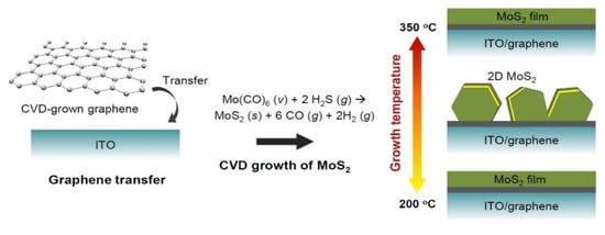
Figure 1.
Schematic of the preparation method for various MoS2 nanostructures on graphene.
2. Experimental
The Graphene was grown on Cu foils (Alfa Aesar) using inductively-coupled plasma chemical vapor deposition (ICP CVD) with CH4 and H2 gases at 950 °C for 5 min. The ICP power and growth pressure were fixed at 200 W and 1 Torr, respectively. The synthesized graphene on Cu was transferred on an ITO glass substrate (Figure 1). The CVD growth and transfer procedures of graphene were described in further detail elsewhere [24]. MoS2 was grown on ITO and ITO/graphene substrates at various temperatures (200 °C, 250 °C, 300 °C, and 350 °C) through MOCVD reaction with Mo(CO)6 and H2S gas (5 vol% in balance N2) as Mo and S precursors, respectively. Mo(CO)6 was vaporized at 20 °C and carried into a quartz reaction tube with Ar gas of 25 standard cubic centimeters per minute (SCCM). The flow rate of H2S gas was 75 SCCM. The growth pressure and time were fixed at 1 Torr and 5 min, respectively.
The morphology and microstructure of MoS2 were characterized via scanning electron microscopy (SEM: Hitachi S-4800, Tokyo, Japan) and transmission electron microscopy (TEM: Tecnai G2 F30 S-Twin, Hillsboro, OR, USA). The crystal structure of MoS2 was characterized by TEM and micro-Raman spectroscopy using an excitation band of 532 nm and a charge-coupled device detector. The optical properties were evaluated by ultraviolet–visible (UV–Vis) spectroscopy (S-3100, SCINCO, Seoul, Korea) and photoluminescence (PL) spectroscopy (excitation at 532 nm). The photo-excited carrier behavior was investigated by time-resolved PL (TRPL) measurements. The samples were excited using a 467 nm pulsed laser and the transient signal was recorded using a time-correlated single photon counting spectrometer (Horiba Fluorolog 3, Kyoto, Japan). The energy level of MoS2 was evaluated via UV photoelectron spectroscopy (UPS; Thermo scientific, K-alpha+, Waltham, MA, USA).
PEC cells were fabricated on 1 × 2 cm2 ITO and ITO/graphene substrates. The working area of the PEC cells was fixed at 0.5 × 0.5 cm2 using nonconductive epoxy to cover undesired areas. PEC characterization was performed using a three-electrode system and an electrochemical analyzer (potentiostat/galvanostat 263A, HS Technologies, Gyeonggi-do, Korea). A Pt plate and KCl-saturated calomel (Hg/Hg2Cl2) were used as counter and reference electrodes, respectively. The electrolyte solution was prepared with 0.3 M KH2PO4 in KOH solution (pH 6.5). The light source used was a 150 W Xe arc lamp that delivered an intensity of 100 mW/cm2 of simulated AM 1.5 G irradiation. The current density–voltage characteristics were recorded using a source meter (Keithley 2400, Cleveland, OH, USA). Electrochemical impedance spectroscopy (EIS) measurement was performed under constant light illumination (100 mW/cm2) at a bias of 0.6 V while varying the AC frequency from 100 kHz to 100 mHz.
3. Results and Discussion
The morphology of MoS2 grown on graphene was crucially affected by the growth temperature of the MOCVD process. At 200 °C, an MoS2 film with a thickness of ~50 nm was formed, hereinafter referred to as G/MoS2-200 (Figure 2a). When the growth temperature was increased to 250 °C, the MoS2 morphology drastically changed to vertically aligned nanosheets with a height of ~200 nm and length of ~150–250 nm, hereinafter referred to as G/MoS2-250 (Figure 2b). The MoS2 nanosheets were vertically aligned and densely packed on the ITO/graphene substrate, which is ideal for PEC photoelectrode applications due to its high specific surface area of 2D MoS2 catalytic edge sites. Theoretical and experimental results indicate that the strong catalytic activity of 2D MoS2 arises from active S atom sites exposed along the edges [3,4,5]. The height of the vertically aligned MoS2 nanosheets increased further to ~250 nm at 300 °C, hereinafter referred to as G/MoS2-300 (Figure 2c). However, above 350 °C, the morphology of MoS2 changed back to a ~130 nm-thick film, hereinafter referred to as G/MoS2-350 (Figure 2d). The size of 2D layered MoS2 nanosheets (S–Mo–S) seemed to be determined by the migration length of impinged Mo adatoms, which bonds two S anions in S-stabilized growth condition. The height of the G/MoS2-300 nanosheet was higher than that of G/MoS2-250 because of the enhanced migration length of Mo adatoms at a higher growth temperature. When the growth temperature was increased further, the ratio of Mo to S adatoms also increased due to the predominant desorption of S adatoms from the growth front surface. Under S-deficient conditions, impinged Mo adatoms tended to bond immediately with the nearest Mo adatoms. As a result, a thin film morphology composed of particles was observed at 350 °C [8,25,26].
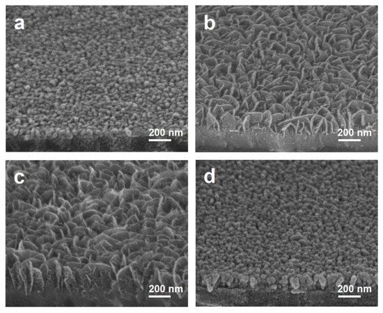
Figure 2.
SEM images of MoS2 nanostructures synthesized on graphene at various growth temperatures: (a) G/MoS2-200 at 200 °C, (b) G/MoS2-250 at 250 °C, (c) G/MoS2-300 at 300 °C, and (d) G/MoS2-350 at 350 °C.
The structures of MoS2 and graphene were investigated using Raman spectroscopy and TEM. The Raman spectrum of pristine CVD-grown graphene showed a low-intensity ratio of D to G band peaks (>0.15) (Figure 3a). The light transmittance of 96.8 % at 550 nm (Figure S1 in Supporting Information) corresponds to approximately one and a half layers of high-quality graphene [24]. The graphene layer was still present after the MOCVD growth of MoS2, as confirmed by the presence of characteristic G and 2D band peaks in the Raman spectrum (Figure 3a). All the graphene/MoS2 samples exhibited the E12g mode and A1g mode in Raman spectra (Figure 3b). The E12g and A1g modes are attributed to the in-plane vibration of Mo and S atoms and the out-of-plane vibration of S atoms, respectively. The number of MoS2 layers can be estimated from the positions and relative frequency difference (RFD) of the E12g and A1g peaks [27,28]. For G/MoS2-250, the RFD value (22.3 cm−1) of E12g (385.0 cm−1) and A1g peaks (407.3 cm−1) corresponds to a few layers of MoS2. The increased RFD value (24.0 cm−1) with a blue-shifted A1g peak (409.3 cm−1) of G/MoS2-300 indicates a slightly increased number of layers. The blue-shifted A1g mode is attributed to the increased restoring force of the interlayer S–S atoms due to the increased number of layers. The thin film samples (G/MoS2-200 and G/MoS2-350) exhibited further increased RFD values with more-blue-shifted A1g modes (inset in Figure 3b). The TEM images of G/MoS2-250 showed that the MoS2 nanosheets have a layered structure (Figure 2c). The nanosheets comprised several (1–5) layers with an interlayer spacing of 0.63 nm, corresponding to semiconducting 2H MoS2 (Figure 2d). Meanwhile, the MoS2 nanosheets grown on ITO at 250 °C, hereinafter referred to as ITO/MoS2-250, exhibited similar size and morphology as the counterpart sample, G/MoS2-250 (Figure S2a). The RFD value of the E12g and A1g peaks of ITO/MoS2-250 was also nearly the same as that of G/MoS2-250 (Figure S2b).
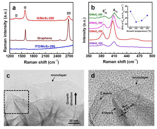
Figure 3.
(a) Raman spectra of ITO/MoS2-250, G/MoS2-250, and pristine graphene. (b) Raman spectra of G/MoS2-200, G/MoS2-250, G/MoS2-300, and G/MoS2-350. The inset shows the RFD between the E12g and A1g Raman modes. (c,d) low-magnification and high-resolution TEM images of MoS2 nanosheets of G/MoS2-250, respectively.
The PEC activities of the MoS2 samples were evaluated by recording linear sweep voltammograms in the dark and under simulated AM 1.5 G illumination. Compared with ITO/MoS2-250, G/MoS2-250 showed significantly higher PEC photocurrent density through the measured potential range (Figure 4a), whereas the dark currents of the two samples were comparable to each other (Figure S3). Therefore, G/MoS2-250 yielded approximately three times higher photoconversion efficiency (0.76% at 0.45 V) than ITO/MoS2-250 (0.22% at 0.7 V), as shown in Figure 4b. The photoconversion efficiency of G/MoS2-250 was comparable with various recently reported photoanodes, such as TiO2/MoS2 [9,29,30], ZnO/MoS2 [31], CoTe/MoS2 [32], and MoS2/α-Fe2O3 [33]. Moreover, the long-term stability of MoS2 flakes was significantly improved by forming a heterojunction with graphene (Figure 4c). The photocurrent of G/MoS2-250 did not change significantly through 1 h of illumination, whereas the photocurrent of ITO/MoS2-250 decreased continuously. The decayed photocurrent of ITO/MoS2-250 can be attributed to the decomposition of MoS2, mainly the loss of S elements [8]. The improved stability can be attributed to the effective separation and transfer of the photogenerated e–h pairs in the heterojunction [8]. Among the graphene/MoS2 samples, the vertically aligned MoS2 nanosheet samples (G/MoS2-250 and G/MoS2-300) yielded significantly higher photocurrent densities compared with the MoS2 thin film samples (G/MoS2-200 and G/MoS2-350). PEC activity was also significantly affected by the size of the few-layer MoS2 nanosheet. Despite its larger MoS2 nanosheet size, G/MoS2-300 yielded a lower photocurrent density than G/MoS2-250. Our previous study on MoS2 nanosheets on TiO2 nanowires demonstrated that for PEC applications, the optimum size of MoS2 nanosheets seemed to depend on the diffusion length of the carriers (~0.34 and ~0.24 μm for electrons and holes, respectively) [18].
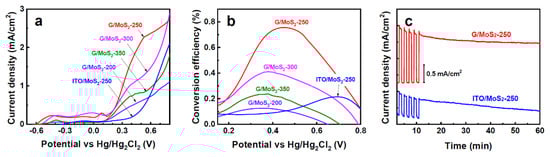
Figure 4.
(a) Photocurrent density–potential curves and (b) photoconversion efficiency–potential curves of PEC cells with various working electrodes (ITO/MoS2-250, G/MoS2-200, G/MoS2-250, G/MoS2-300, and G/MoS2-350). (c) Photocurrent–time plots for ITO/MoS2-250 and G/MoS2-250 at 0.6 V.
To investigate the electronic transitions and charge transport properties of MoS2 nanosheet samples, systematic studies, including EIS, UV–Vis absorption, PL, and TRPL spectroscopy, were conducted. G/MoS2-250 and ITO/MoS2-250 showed nearly the same UV–Vis absorption spectra with two prominent peaks at approximately 607 nm and 663 nm (Figure 5a). The two peaks, known as excitons B and A, respectively, can be attributed to the direct excitonic transitions at the K point of the MoS2 Brillouin zone [8,34]. The absorption difference of the two samples resulted from only the optical absorption of the graphene layer (<5%).
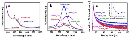
Figure 5.
(a) UV–Vis absorption spectra of ITO/MoS2-250, G/MoS2-250, and pristine graphene. (b) PL spectra and (c) TRPL results of ITO/MoS2-250, G/MoS2-200, G/MoS2-250, G/MoS2-300, and G/MoS2-350. The inset in (c) shows the carrier lifetimes extracted from corresponding TRPL measurements.
Both samples exhibited a PL peak at 676 nm (Figure 5b), which is consistent with the energy of exciton A, suggesting that a dominant electronic transition was the direct bandgap transitions at the K point. G/MoS2-300 showed a main PL peak at 676 nm, with a satellite peak at 705 nm. The thin film samples (G/MoS2-200 and G/MoS2-350) yielded a red-shifted PL peak at 705 nm with respect to G/MoS2-250. The PL around 705 nm is attributed to the indirect bandgap transitions of the MoS2 bulk form. All graphene/MoS2 samples achieved significantly lower PL efficiencies than ITO/MoS2-250. The considerable PL quenching can be attributed to the reduced recombination of e–h pairs through the heterojunction of graphene/MoS2. The dynamic behavior of photo-generated carriers was further investigated by TRPL spectroscopy (Figure 5c). The average carrier lifetimes were extracted by the PL decay kinetics fitted by a bi-exponential decay profile [35]. G/MoS2-250 exhibited the shortest carrier lifetime of 3.09 ns, whereas ITO/MoS2-250 showed the longest carrier lifetime of 4.23 ns (inset in Figure 5c). The reduced carrier lifetime indicates that the heterojunction of graphene/MoS2 is beneficial to the efficient separation and transport of photo-generated carriers to the semiconductor/liquid interface [14]. In addition, the few-layer MoS2 nanosheet samples (G/MoS2-250 and G/MoS2-300) exhibited shorter carrier lifetimes than the thin film samples (G/MoS2-200 and G/MoS2-350), suggesting that vertically aligned nanosheets provided more efficient carrier transport paths, i.e., they have highly conductive edges compared with the bulk form.
Figure 6a shows the Nyquist plots of the EIS spectra of G/MoS2-250 and ITO/MoS2-250 in the dark and under illumination. G/MoS2-250 showed smaller EIS semicircles than ITO/MoS2-250, whose radius mirrors the charge transfer resistance (Rct), indicating that the graphene layer significantly enhanced the charge transfer efficiency. The Nyquist plots can be fitted using a simplified Randles circuit (inset in Figure 6a), which consists of Rct, solution resistance (Rs), constant phase element (Q), and diffusion of species in electrolyte solution represented by Warburg impedance (W). G/MoS2-250 yielded values of 3196 Ω and 2069 Ω for Rct in the dark and under illumination, respectively, whereas ITO/MoS2-250 exhibited Rct values of 4597 Ω and 3166 Ω. Moreover, the Rct (dark) to Rct (photo) ratio (1.55) of G/MoS2-250 was greater than that of ITO/MoS2-250 (1.45), suggesting that graphene/MoS2 heterojunction was more beneficial under illumination than in the dark. G/MoS2-250 and G/MoS2-300 showed smaller EIS semicircles than G/MoS2-350, indicating a decrease in Rct and suppression of charge recombination (Figure 6b). The improved PEC activity and lower Rct can be attributed to the desirable vertically aligned architecture, which provided highly conductive edges as an efficient pathway for photo-generated carriers and better electronic contact with graphene substrates [16].
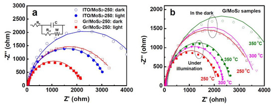
Figure 6.
(a) Nyquist plots of ITO/MoS2-250 and G/MoS2-250 in the dark and under illumination. The inset shows an equivalent Randles circuit. (b) Nyquist plots of G/MoS2-250, G/MoS2-300, and G/MoS2-350.
To understand the carrier transport property across the heterojunction of graphene/MoS2, its electronic structure was studied via UPS. Figure 7a,b shows the UPS secondary electron cut-off and valence spectra of G/MoS2-250, respectively. The work function of MoS2 was 4.76 ± 0.15 eV, which can be determined by the difference between the photon energy of excited radiation (21.2 eV) and the spectrum width, which is measured from the valence band and secondary edges (16.44 eV, Figure 7a). The energy difference between the Fermi level and valence band edge (EF−EVB) was 1.50 eV (Figure 7b). Considering the bandgap energy of ~1.88 eV for MoS2 determined by the UV–Vis absorption and PL spectra, the electron affinity (χ) of MoS2 was approximately 4.38 eV, which is consistent with previously reported values (~4.3 eV) [36]. The estimated electronic structure of MoS2 nanosheets is shown in the inset of Figure 7b. The Fermi level of MoS2 is close to the Fermi level (~4.6–4.8 eV of work function) of pristine few-layer graphene [37], resulting in a small built-in potential barrier for electron transport (Figure 7c). Consequently, G/MoS2-250 exhibited a small positive water oxidation onset potential (~0.18 V, as shown in Figure 4a), which is generally defined by the potential at the intersection of the dark current and the tangent at the maximum slope of the photocurrent. By contrast, ITO/MoS2-250 showed a water oxidation onset potential of ~0.49 V, implying a larger built-in potential barrier for electron transport (Figure 7c). The appropriately located Fermi level of graphene between the Fermi level of ITO and the conduction band edge of MoS2 is another benefit of the graphene/MoS2 heterostructure for the efficient extraction of electrons to the cathode (Figure 7d).
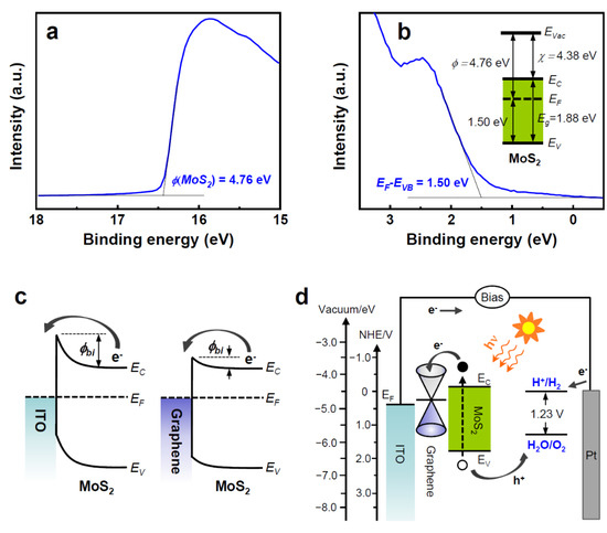
Figure 7.
(a) UPS secondary electron cut-off and (b) valence spectra of G/MoS2-250. The inset in (b) shows the corresponding energy band diagram of 2D MoS2 nanosheets on graphene. (c) Energy band diagrams of the Schottky junctions of ITO/MoS2 and graphene/MoS2. (d) PEC water-splitting working principle of 2D MoS2 nanosheets on graphene.
4. Conclusions
We demonstrated the successful manipulation of MoS2 morphology from thin film to vertically-aligned few-layer nanosheets on graphene in a controllable and practical manner using MOCVD. Desirable vertical few-layer MoS2 nanosheets were synthesized on graphene at relatively low temperatures (250–300 °C). Low-temperature growth was beneficial to the formation of high-quality graphene/MoS2 heterojunctions, which not only significantly enhanced the charge transfer resistance but also exhibited cathodic-shifted water oxidation onset potential (~0.18 V) by lowering a built-in potential barrier for electron transport. As a result, G/MoS2-250 showed approximately three times higher photoconversion efficiency (0.76% at 0.45 V) than ITO/MoS2-250 (0.22% at 0.7 V). The best PEC performance of G/MoS2-250 resulted from the combined effect of (i) a favorable graphene/MoS2 heterojunction, through which photo-generated e–h pairs were efficiently separated and transported; (ii) a desirable architecture of vertically aligned few-layer MoS2 nanosheets, which provided highly conductive edges that serve as efficient carrier pathways and better electronic contact with the graphene substrate; and (iii) a controlled height of few-layer MoS2 nanosheets within the diffusion length of the carriers. These results not only provide the optimal morphology of MoS2 for exploiting the full potential of 2D MoS2 for various PEC applications, but also demonstrate a practical large-scale and controllable 2D MoS2 synthesis approach on graphene.
Supplementary Materials
The following are available online at https://www.mdpi.com/article/10.3390/nano11061585/s1, Figure S1: UV–Vis absorption spectrum of pristine graphene, exhibiting a light transmittance of 96.88 % at 550 nm, Figure S2: (a) SEM image of few-layer MoS2 nanosheets grown on ITO (ITO/MoS2-250). (b) Raman spectra of ITO/MoS2-250, G/MoS2-250, and pristine graphene, Figure S3: Dark current density–potential curves of PEC cells with various working electrodes (ITO/MoS2-250, G/MoS2-200, G/MoS2-250, G/MoS2-300, and G/MoS2-350).
Author Contributions
Conceptualization, E.-T.K.; Data curation, D.-B.S. and E.-T.K.; Formal analysis, E.-T.K.; Methodology, D.-B.S. and S.-S.B.; Software, T.N.T., E.-T.K. and D.-B.S.; Supervision, E.-T.K.; Visualization, E.-T.K.; Writing—Original draft: E.-T.K.; Writing—Review and Editing: E.-T.K. All authors have read and agreed to the published version of the manuscript.
Funding
This research was supported by the National Research Foundation of Korea (NRF) grants funded by the Korea government (MSIT) (2020R1A4A4079397 and 2021R1A2C1006241) and the Ministry of Education (2019R1A6A3A13095792).
Data Availability Statement
Data are available in the main text.
Conflicts of Interest
The authors declare no conflict of interest.
References
- Zhou, M.; Lou, X.W.; Xie, Y. Two-dimensional nanosheets for photoelectrochemical water splitting: Possibilities and opportunities. Nano Today 2013, 8, 598–618. [Google Scholar] [CrossRef]
- Faraji, M.; Yousefi, M.; Yousefzadeh, S.; Zirak, M.; Naseri, N.; Jeon, T.H.; Choi, W.; Moshfegh, A.Z. Two-dimensional materials in semiconductor photoelectrocatalytic systems for water splitting. Energy Environ. Sci. 2019, 12, 59–95. [Google Scholar] [CrossRef]
- Ding, Q.; Song, B.; Xu, P.; Jin, S. Efficient electrocatalytic and photoelectrochemical hydrogen generation using MoS2 and related compounds. Chem 2016, 1, 699–726. [Google Scholar] [CrossRef]
- Han, B.; Hu, Y.H. MoS2 as a co-catalyst for photocatalytic hydrogen production from water. Energy Sci. Eng. 2016, 4, 285–304. [Google Scholar] [CrossRef]
- Chen, B.; Meng, Y.; Sha, J.; Zhong, C.; Hu, W.; Zhao, N. Preparation of MoS2/TiO2 based nanocomposites for photocatalysis and rechargeable batteries: Progress, challenges, and perspective. Nanoscale 2018, 10, 34–68. [Google Scholar] [CrossRef]
- Lamouchi, A.; Assaker, I.B.; Chtourou, R. Enhanced photoelectrochemical activity of MoS2-decorated ZnO nanowires electrodeposited onto stainless steel mesh for hydrogen production. Appl. Surf. Sci. 2019, 478, 937–945. [Google Scholar] [CrossRef]
- Liu, Y.; Yu, Y.X.; Zhang, W.D. MoS2/CdS heterojunction with high photoelectrochemical activity for H2 evolution under visible light: The role of MoS2. J. Phys. Chem. C 2013, 117, 12949–12957. [Google Scholar] [CrossRef]
- Trung, T.N.; Seo, D.B.; Quang, N.D.; Kim, D.; Kim, E.T. Enhanced photoelectrochemical activity in the heterostructure of vertically aligned few-layer MoS2 flakes on ZnO. Electrochim. Acta 2018, 260, 150–156. [Google Scholar] [CrossRef]
- Pi, Y.; Li, Z.; Xu, D.; Liu, J.; Li, Y.; Zhang, F.; Zhang, G.; Peng, W.; Fan, X. 1T-phase MoS2 nanosheets on TiO2 nanorod arrays: 3D photoanode with extraordinary catalytic performance. ACS Sustain. Chem. Eng. 2017, 5, 5175–5182. [Google Scholar] [CrossRef]
- Huang, Z.; Han, W.; Tang, H.; Ren, L.; Chander, D.S.; Qi, X.; Zhang, H. Photoelectrochemical-type sunlight photodetector based on MoS2/graphene heterostructure. 2D Mater. 2015, 2, 035011. [Google Scholar] [CrossRef]
- Carraro, F.; Calvillo, L.; Cattelan, M.; Favaro, M.; Righetto, M.; Nappini, S.; Píš, I.; Celorrio, V.; Fermín, D.J.; Martucci, A.; et al. Fast one-pot synthesis of MoS2/crumpled graphene p–n nanonjunctions for enhanced photoelectrochemical hydrogen production. ACS Appl. Mater. Interfaces 2015, 7, 25685–25692. [Google Scholar] [CrossRef]
- Geim, A.K.; Novoselov, K.S. The rise of graphene. Nat. Mater. 2007, 6, 183–191. [Google Scholar] [CrossRef]
- Chang, K.; Mei, Z.; Wang, T.; Kang, Q.; Ouyang, S.; Ye, J. MoS2/graphene cocatalyst for efficient photocatalytic H2 evolution under visible light irradiation. ACS Nano 2014, 8, 7078–7087. [Google Scholar] [CrossRef]
- Yu, X.; Du, R.; Li, B.; Zhanga, Y.; Liu, H.; Qu, J.; An, X. Biomolecule-assisted self-assembly of CdS/MoS2/graphene hollowspheres as high-efficiency photocatalysts for hydrogen evolution without noble metals. Appl. Catal. B 2016, 182, 504–512. [Google Scholar] [CrossRef]
- Zhang, Y.; Du, J.; Wang, Z.; Luo, M.; Tian, Y.; Fujita, T.; Xue, Q.; Chen, M. Three-dimensional nanoporous heterojunction of monolayer MoS2@rGO for photoenhanced hydrogen evolution reaction. ACS Appl. Energy Mater. 2018, 1, 2183−2191. [Google Scholar] [CrossRef]
- He, H.; Lin, J.; Fu, W.; Wang, X.; Wang, H.; Zeng, Q.; Gu, Q.; Li, Y.; Yan, C.; Tay, B.K.; et al. MoS2/TiO2 edge-on heterostructure for efficient photocatalytic hydrogen evolution. Adv. Energy Mater. 2016, 6, 1600464. [Google Scholar] [CrossRef]
- Seo, D.B.; Trung, T.N.; Kim, D.O.; Duc, D.V.; Hong, S.; Sohn, Y.; Jeong, J.R.; Kim, E.T. Plasmonic Ag-decorated few-layer MoS2 nanosheets vertically grown on graphene for efficient photoelectrochemical water splitting. Nano Micro Lett. 2020, 12, 172. [Google Scholar] [CrossRef]
- Seo, D.B.; Kim, S.; Trung, T.N.; Kim, D.; Kim, E.T. Conformal growth of few-layer MoS2 flakes on closely-packed TiO2 nanowires and their enhanced photoelectrochemical reactivity. J. Alloys Compd. 2019, 770, 686–691. [Google Scholar] [CrossRef]
- Lu, Z.; Zhu, W.; Yu, X.; Zhang, H.; Li, Y.; Sun, X.; Wang, X.; Wang, H.; Wang, J.; Luo, J.; et al. Ultrahigh hydrogen evolution performance of under-water “Superaerophobic” MoS2 nanostructured electrodes. Adv. Mater. 2014, 26, 2683–2687. [Google Scholar] [CrossRef] [PubMed]
- Lee, C.; Yan, H.; Brus, L.E.; Heinz, T.F.; Hone, J.; Ryu, S. Anomalous lattice vibrations of single- and few-layer MoS2. ACS Nano 2010, 4, 2695–2700. [Google Scholar] [CrossRef] [PubMed]
- Li, H.; Zhang, Q.; Yap, C.C.R.; Tay, B.K.; Edwin, T.H.T.; Olivier, A.; Baillargeat, D. From bulk to monolayer MoS2: Evolution of raman scattering. Adv. Funct. Mater 2012, 22, 1385–1390. [Google Scholar] [CrossRef]
- Mak, K.F.; Lee, C.; Hone, J.; Shan, J.; Heinz, T.F. Atomically thin MoS2: A new direct-gap semiconductor. Phys. Rev. Lett. 2010, 105, 136805. [Google Scholar] [CrossRef]
- Velický, M.; Bissett, M.A.; Woods, C.R.; Toth, P.S.; Georgiou, T.; Kinloch, I.A.; Novoselov, K.S.; Dryfe, R.A.W. Photoelectrochemistry of pristine mono- and few-layer MoS2. Nano Lett. 2016, 16, 2023–2032. [Google Scholar] [CrossRef] [PubMed]
- Nang, L.V.; Kim, E.T. Controllable synthesis of high-quality graphene using inductively coupled plasma chemical vapor deposition. J. Electrochem. Soc. 2012, 159, K93−K96. [Google Scholar] [CrossRef]
- Kang, K.; Xie, S.; Huang, L.; Han, Y.; Huang, P.Y.; Mak, K.F.; Kim, C.J.; Muller, D.; Park, J. High-mobility three-atom-thick semiconducting films with wafer-scale homogeneity. Nature 2015, 520, 656–660. [Google Scholar] [CrossRef]
- Lee, Y.H.; Zhang, X.Q.; Zhang, W.; Chang, M.T.; Lin, C.T.; Chang, K.D.; Yu, Y.C.; Wang, J.T.W.; Chang, C.S.; Li, L.J.; et al. Synthesis of large-area MoS2 atomic layers with chemical vapor deposition. Adv. Mater. 2012, 24, 2320–2325. [Google Scholar] [CrossRef] [PubMed]
- Jeon, J.; Jang, S.K.; Jeon, S.M.; Yoo, G.; Jang, Y.H.; Park, J.H.; Lee, S. Layer-controlled CVD growth of large-area two-dimensional MoS2 films. Nanoscale 2015, 7, 1688–1695. [Google Scholar] [CrossRef]
- Yim, C.; O’Brien, M.; McEvoy, N.; Winters, S.; Mirza, I.; Lunney, J.G.; Duesberg, G.S. Investigation of the optical properties of MoS2 thin films using spectroscopic ellipsometry. Appl. Phys. Lett. 2014, 104, 103114. [Google Scholar] [CrossRef]
- Dong, J.; Zhang, X.; Huang, J.; Gao, S.; Mao, J.; Cai, J.; Chen, Z.; Sathasivam, S.; Carmalt, C.J.; Lai, Y. Boosting heterojunction interaction in electrochemical construction of MoS2 quantum dots@TiO2 nanotube arrays for highly effective photoelectrochemical performance and electrocatalytic hydrogen evolution. Electrochem. Commun. 2018, 93, 152–157. [Google Scholar] [CrossRef]
- Han, J.; Zhang, S.; Song, Q.; Yan, H.; Kang, J.; Guo, Y.; Liu, Z. The synergistic effect with S-vacancies and built-in electric field on a TiO2/MoS2 photoanode for enhanced photoelectrochemical performance. Sustain. Energy Fuels 2021, 5, 509–517. [Google Scholar] [CrossRef]
- Karmakar, K.; Maity, D.; Pal, D.; Mandal, K.; Khan, G.G. Photo-induced exciton dynamics and broadband light harvesting in ZnO nanorod-templated multilayered two-dimensional MoS2/MoO3 photoanodes for solar fuel generation. ACS Appl. Nano Mater. 2020, 3, 1223−1231. [Google Scholar] [CrossRef]
- Sitara, E.; Nasir, H.; Mumtaz, A.; Ehsan, M.F.; Sohail, M.; Iram, S.; Bukhari, S.A.B. Efficient photoelectrochemical water splitting by tailoring MoS2/CoTe heterojunction in a photoelectrochemical cell. Nanomaterials 2020, 10, 2341. [Google Scholar] [CrossRef]
- Masoumi, Z.; Tayebi, M.; Lee, B.K. Ultrasonication-assisted liquid-phase exfoliation enhances photoelectrochemical performance in α-Fe2O3/MoS2 photoanode. Ultrason. Sonochem. 2021, 72, 105403. [Google Scholar] [CrossRef]
- Eda, G.; Yamaguchi, H.; Voiry, D.; Fujita, T.; Chen, M.; Chhowalla, M. Photoluminescence from chemically exfoliated MoS2. Nano Lett. 2011, 11, 5111–5116. [Google Scholar] [CrossRef]
- Major, J.D.; Al Turkestani, M.; Bowen, L.; Brossard, M.; Li, C.; Lagoudakis, P.; Pennycook, S.J.; Phillips, L.J.; Treharne, R.E.; Durose, K. In-depth analysis of chloride treatments for thin-film CdTe solar cells. Nat. Commun. 2016, 7, 13231. [Google Scholar] [CrossRef]
- Lee, H.; Deshmukh, S.; Wen, J.; Costa, V.Z.; Schuder, J.S.; Sanchez, M.; Ichimura, A.A.; Pop, E.; Wang, B.; Newqaz, A.K.M. Layer-dependent interfacial transport and optoelectrical properties of MoS2 on ultraflat metals. ACS Appl. Mater. Interfaces 2019, 11, 31543−31550. [Google Scholar] [CrossRef] [PubMed]
- Yu, Y.J.; Zhao, Y.; Ryu, S.; Brus, L.E.; Kim, K.S.; Kim, P. Tuning the graphene work function by electric field effect. Nano Lett. 2009, 9, 3430–3434. [Google Scholar] [CrossRef] [PubMed]


Publisher’s Note: MDPI stays neutral with regard to jurisdictional claims in published maps and institutional affiliations. |
© 2021 by the authors. Licensee MDPI, Basel, Switzerland. This article is an open access article distributed under the terms and conditions of the Creative Commons Attribution (CC BY) license (https://creativecommons.org/licenses/by/4.0/).