
Growth and Characterisation Studies of Eu3O4 Thin Films Grown on Si/SiO2 and Graphene

 , , ,
, , ,
Abstract
:1. Introduction
2. Materials and Methods
3. Results and Discussion
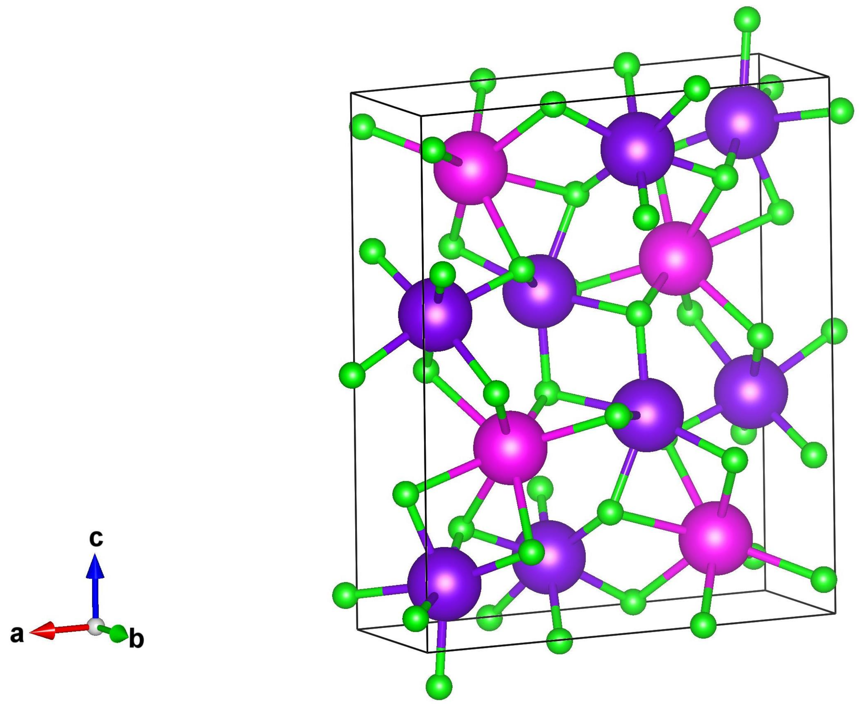
3.1. X-ray Diffraction and Reflection (XRD and XRR)
3.2. SQUID
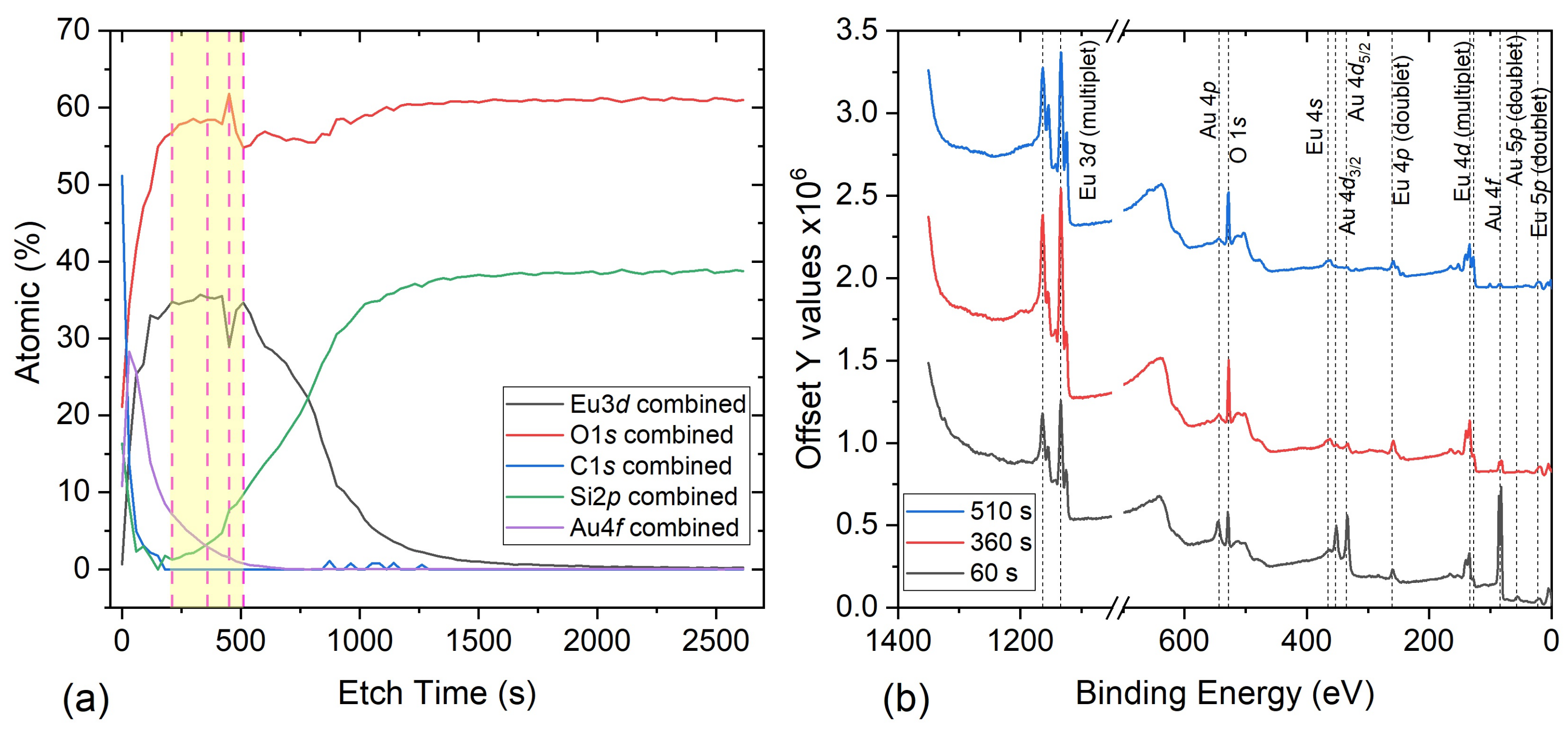
3.3. XPS
3.4. Raman Spectroscopy
4. Conclusions
Author Contributions
Funding
Institutional Review Board Statement
Informed Consent Statement
Data Availability Statement
Acknowledgments
Conflicts of Interest
References
- Varma, C.M. Mixed-valence compounds. Rev. Mod. Phys. 1976, 48, 219–238. [Google Scholar] [CrossRef]
- Rau, R.C. The crystal structure of Eu3O4. Acta Crystallogr. 1966, 20, 716–723. [Google Scholar] [CrossRef]
- Ahn, K.; Pecharsky, V.K.; Gschneidner, K.A. The magnetothermal behavior of mixed-valence Eu3O4. J. Appl. Phys. 2009, 106, 043918. [Google Scholar] [CrossRef]
- Holmes, L.; Schieber, M. Magnetic Ordering in Eu3O4 and EuGd2O4. J. Appl. Phys. 1966, 37, 968–969. [Google Scholar] [CrossRef]
- Holmes, L.; Schieber, M. Metamagnetism in Eu3O4. Phys. Rev. 1968, 167, 449–457. [Google Scholar] [CrossRef]
- Momma, K.; Izumi, F. VESTA 3 for three-dimensional visualization of crystal, volumetric and morphology data. J. Appl. Crys. 2011, 44, 1272–1276. [Google Scholar] [CrossRef]
- Avsar, A.; Yang, T.Y.; Bae, S.; Balakrishnan, J.; Volmer, F.; Jaiswal, M.; Yi, Z.; Ali, S.R.; Guöntherodt, G.; Hong, B.H.; et al. Toward wafer scale fabrication of graphene based spin valve devices. Nano Lett. 2011, 11, 2363–2368. [Google Scholar] [CrossRef] [PubMed] [Green Version]
- Ahn, E.C. 2D materials for spintronic devices. NPJ 2D Mater. Appl. 2020, 4. [Google Scholar] [CrossRef]
- Rybkina, A.A.; Rybkin, A.G.; Klimovskikh, I.I.; Skirdkov, P.N.; Zvezdin, K.A.; Zvezdin, A.K.; Shikin, A.M. Advanced graphene recording device for spin-orbit torque magnetoresistive random access memory. Nanotechnology 2020, 31. [Google Scholar] [CrossRef] [PubMed]
- Averyanov, D.V.; Sokolov, I.S.; Tokmachev, A.M.; Parfenov, O.E.; Karateev, I.A.; Taldenkov, A.N.; Storchak, V.G. High-Temperature Magnetism in Graphene Induced by Proximity to EuO. ACS Appl. Mater. Interfaces 2018, 10, 20767–20774. [Google Scholar] [CrossRef]
- Klinkhammer, J.; Forster, D.F.; Schumacher, S.; Oepen, H.P.; Michely, T.; Busse, C. Structure and magnetic properties of ultra thin textured EuO films on graphene. Appl. Phys. Lett. 2013, 103, 10–15. [Google Scholar] [CrossRef]
- Klinkhammer, J.; Schlipf, M.; Craes, F.; Runte, S.; Michely, T.; Busse, C. Spin-Polarized Surface State in EuO(100). Phys. Rev. Lett. 2014, 112, 016803. [Google Scholar] [CrossRef] [Green Version]
- Hallal, A.; Ibrahim, F.; Yang, H.; Roche, S.; Chshiev, M. Tailoring magnetic insulator proximity effects in graphene: First-principles calculations. 2D Mater. 2017, 4, 025074. [Google Scholar] [CrossRef]
- Song, Y.; Dai, G. Spin filter and spin valve in ferromagnetic graphene. Appl. Phys. Lett. 2015, 106, 223104. [Google Scholar] [CrossRef] [Green Version]
- Yang, H.X.; Hallal, A.; Terrade, D.; Waintal, X.; Roche, S.; Chshiev, M. Proximity Effects Induced in Graphene by Magnetic Insulators: First-Principles Calculations on Spin Filtering and Exchange-Splitting Gaps. Phys. Rev. Lett. 2013, 110, 046603. [Google Scholar] [CrossRef] [PubMed] [Green Version]
- Su, S.; Barlas, Y.; Li, J.; Shi, J.; Lake, R.K. Effect of intervalley interaction on band topology of commensurate graphene/EuO heterostructures. Phys. Rev. B 2017, 95, 075418. [Google Scholar] [CrossRef] [Green Version]
- Solis, D.A.; Hallal, A.; Waintal, X.; Chshiev, M. Proximity magnetoresistance in graphene induced by magnetic insulators. Phys. Rev. B 2019, 100, 104402. [Google Scholar] [CrossRef] [Green Version]
- Mauger, A.; Godart, C. The Magnetic, Optical, and Transport Properties of Representatives of a Class of Magnetic Semiconductors: The Europium Chalcogenides. Phys. Rep. 1986, 141, 51–176. [Google Scholar] [CrossRef]
- Steeneken, P.G. New light on EuO thin films: Preparation, transport, magnetism and spectroscopy of a ferromagnetic semiconductor. arXiv 2012, arXiv:1203.6771. [Google Scholar]
- Averyanov, D.V.; Tokmachev, A.M.; Parfenov, O.E.; Karateev, I.A.; Sokolov, I.S.; Taldenkov, A.N.; Platunov, M.S.; Wilhelm, F.; Rogalev, A.; Storchak, V.G. Probing proximity effects in the ferromagnetic semiconductor EuO. Appl. Surf. Sci. 2019, 488, 107–114. [Google Scholar] [CrossRef]
- Santos, T.S.; Moodera, J.S.; Raman, K.V.; Negusse, E.; Holroyd, J.; Dvorak, J.; Liberati, M.; Idzerda, Y.U.; Arenholz, E. Determining Exchange Splitting in a Magnetic Semiconductor by Spin-filter Tunneling. Phys. Rev. Lett. 2008, 101, 147201. [Google Scholar] [CrossRef] [Green Version]
- Santos, T.S.; Moodera, J.S. Observation of spin filtering with a ferromagnetic EuO tunnel barrier. Phys. Rev. B Condens. Matter Mater. Phys. 2004, 69, 241203. [Google Scholar] [CrossRef]
- Ohsugi, R.; Omi, H.; Krockenberger, Y.; Fujiwara, A. Spin splitting in EuO(111)/Si(111) spin-filter tunnel junctions with atomically sharp interface. Jpn. J. Appl. Phys. 2018, 57, 2–5. [Google Scholar] [CrossRef]
- Monteiro, P.M.S.; Baker, P.J.; Hine, N.D.M.; Steinke, N.J.; Ionescu, A.; Cooper, J.F.K.; Barnes, C.H.W.; Kinane, C.J.; Salman, Z.; Wildes, A.R.; et al. The Elevated Curie Temperature and Half-metallicity in the Ferromagnetic Semiconductor LaxEu1-xO. Phys. Rev. B 2015, 92, 045202. [Google Scholar] [CrossRef] [Green Version]
- Monteiro, P.M.S.; Baker, P.J.; Ionescu, A.; Barnes, C.H.W.; Salman, Z.; Suter, A.; Prokscha, T.; Langridge, S. Spatially Homogeneous Ferromagnetism Below The Enhanced Curie Temperature in EuO1-x Thin Films. Phys. Rev. Lett. 2013, 110, 217208. [Google Scholar] [CrossRef] [PubMed] [Green Version]
- Goian, V.; Held, R.; Bousquet, E.; Yuan, Y.; Melville, A.; Zhou, H.; Gopalan, V.; Ghosez, P.; Spaldin, N.A.; Schlom, D.G.; et al. Making EuO multiferroic by epitaxial strain engineering. Commun. Mater. 2020, 1, 1–10. [Google Scholar] [CrossRef]
- Vitins, J. Inelastic light scattering and photoluminescence in the mixed valence systems Eu3O4, Eu3S4 and Sm3S4. J. Magn. Magn. Mater. 1977, 5, 234–242. [Google Scholar] [CrossRef]
- Batlogg, B.; Kaldis, E.; Schlegel, A.; Wachter, P. Electronic structure of a mixed valence system: Eu3O4. Phys. Rev. B 1975, 12, 3940–3947. [Google Scholar] [CrossRef]
- Jacob, K.T.; Rajput, A. Gibbs Energy of Formation of Eu3O4 and EuO. J. Chem. Eng. Data 2016, 61, 1710–1717. [Google Scholar] [CrossRef]
- Daane, A.H. Magnetic properties of Tb2O2SO4. Phys. Status Solidi 1956, 045132, 16–38. [Google Scholar] [CrossRef]
- Rau, R.C. X-Ray Crystallographic Studies of Europium Oxides and Hydroxides; General Electric Co. Advanced Technology Services: Cincinnati, OH, USA, 1962. [Google Scholar] [CrossRef]
- Liu, P.; Tang, J. Antiferromagnetic coupling in EuO1-x. Phys. Rev. B 2012, 85, 224417. [Google Scholar] [CrossRef] [Green Version]
- Liu, P.; Tang, J. A magnetic polaron model for the enhanced Curie temperature of EuO1-x. J. Phys. Condens. Matter 2013, 25, 125802. [Google Scholar] [CrossRef]
- Caspers, C.; Müller, M.; Gray, A.X.; Kaiser, A.M.; Gloskovskii, A.; Fadley, C.S.; Drube, W.; Schneider, C.M. Chemical stability of the magnetic oxide EuO directly on silicon observed by hard x-ray photoemission spectroscopy. Phys. Rev. Condens. Matter Mater. Phys. 2011, 84, 205217. [Google Scholar] [CrossRef] [Green Version]
- Cho, E.J.; Oh, S.-J.; Suzuki, T.; Kasuya, T. Electronic structure study of Eu intermetallic compounds by photoelectron spectroscopy. J. Electron Spectrosc. Relat. Phenom. 1996, 77, 173–181. [Google Scholar] [CrossRef]
- Mariscal, A.; Quesada, A.; Martín-luengo, A.T.; García, M.A.; Bonanni, A.; Fernández, J.F.; Serna, R. Applied Surface Science Europium monoxide nanocrystalline thin films with high near-infrared transparency. Appl. Surf. Sci. 2018, 456, 980–984. [Google Scholar] [CrossRef] [Green Version]
- Cho, E.J.; Oh, S.J.; Imada, S.; Suga, S.; Suzuki, T.; Kasuya, T. Origin of the high-binding-energy structure in the 3d core-level spectra of divalent Eu compounds. Phys. Rev. B 1995, 51, 10146–10149. [Google Scholar] [CrossRef]
- Orlowski, B.A.; Mickievicius, S.; Osinniy, V.; Nadolny, A.J.; Taliashvili, B. High-energy X-ray photoelectron spectroscopy study of MBE grown (Eu, Gd) Te layers. Nucl. Instrum. Methods Phys. Res. B 2005, 238, 346–352. [Google Scholar] [CrossRef]
- Ohno, Y.; Urata, T. Photoelectron spectra and surface valence fluctuation of Eu in the misfit-layer compound {(EuS)1.15}1.5NbS2. J. Electron Spectrosc. Relat. Phenom. 2002, 125, 171–180. [Google Scholar] [CrossRef]
- Kim, D.; Jeong, J.R.; Jang, Y.; Bae, J.S.; Chung, I.; Liang, R.; Seo, D.K.; Kim, S.J.; Park, J.C. Self-emitting blue and red EuOX (X = F, Cl, Br, I) materials: Band structure, charge transfer energy, and emission energy. Phys. Chem. Chem. Phys. 2019, 21, 1737–1749. [Google Scholar] [CrossRef]
- Cho, E.; Oh, S.J. Surface valence transition in trivalent Eu insulating compounds observed by photoelectron spectroscopy. Phys. Rev. B 1999, 59, 3–6. [Google Scholar] [CrossRef]
- Lupan, O.; Pauporté, T.; Viana, B.; Aschehoug, P.; Ahmadi, M.; Cuenya, B.R.; Rudzevich, Y.; Lin, Y.; Chow, L. Eu-doped ZnO nanowire arrays grown by electrodeposition. Appl. Surf. Sci. 2013, 282, 782–788. [Google Scholar] [CrossRef]
- Faye, D.N.; Biquard, X.; Nogales, E.; Felizardo, M.; Peres, M.; Redondo-Cubero, A.; Auzelle, T.; Daudin, B.; Tizei, L.H.; Kociak, M.; et al. Incorporation of Europium into GaN Nanowires by Ion Implantation. J. Phys. Chem. C 2019, 123, 11874–11887. [Google Scholar] [CrossRef]
- Wang, Y.Y.; Ni, Z.H.; Shen, Z.X.; Wang, H.M.; Wu, Y.H. Interference Enhancement of Raman Signal of Graphene. Appl. Phys. Lett. 2008, 92. [Google Scholar] [CrossRef]
- Chilres, I.; Jauregui, L.A.; Park, W.; Cao, H.; Chen, Y.P. Raman Spectroscopy of Viruses and Viral Proteins. In New Developments in Photon and Materials Research; Jang, J.I., Ed.; Elsevier: Amsterdam, The Netherlands, 2013; Chapter 19; pp. 553–595. [Google Scholar] [CrossRef]
- Allard, A.; Wirtz, L. Graphene on Metallic Substrates: Suppression of the Kohn Anomalies in the Phonon Dispersion. Nano Lett. 2010, 10, 4335–4340. [Google Scholar] [CrossRef]
- Malard, L.M.; Pimenta, M.A.; Dresselhaus, G.; Dresselhaus, M.S. Raman Spectroscopy in Graphene. Phys. Rep. 2009, 473, 51–87. [Google Scholar] [CrossRef]
- Shlimak, I.; Haran, A.; Zion, E.; Havdala, T.; Kaganovskii, Y.; Butenko, A.V.; Wolfson, L.; Richter, V.; Naveh, D.; Sharoni, A.; et al. Raman Scattering and Electrical Resistance of Highly Disordered Graphene. Phys. Rev. B 2015, 91, 045414. [Google Scholar] [CrossRef] [Green Version]
- Aboljadayel, R.O.M.; Love, D.M.; Vaz, C.A.F.; Weatherup, R.S.; Braeuninger-Weimer, P.; Martin, M.B.; Cabrero-Vilatela, A.; Ionescu, A.; Kinane, C.J.; Charlton, T.R.; et al. Determining the Proximity Effect Induced Magnetic Moment in Graphene by Polarised Neutron Reflectivity and X-ray Magnetic Circular Dichroism. arXiv 2021, arXiv:2101.09946. [Google Scholar]
- Cabrero-Vilatela, A.; Weatherup, R.S.; Braeuninger-Weimer, P.; Caneva, S.; Hofmann, S. Towards a General Growth Model for Graphene CVD on Transition Metal Catalysts. Nanoscale 2016, 8, 2149–2158. [Google Scholar] [CrossRef] [Green Version]


| Spectrum | 3d | FWHM | 3d Satellites | 3d | FWHM | 3d Satellites |
|---|---|---|---|---|---|---|
| Eu(eV) | ||||||
| t s | 1125.54 | 5.39 | 1131.26 | 1155.14 | 5.29 | 1160.16 |
| t s | 1124.88 | 5.17 | 1130.64 | 1154.75 | 5.76 | 1160.04 |
| t s | 1124.78 | 5.01 | 1131.19 | 1154.65 | 5.64 | 1159.96 |
| t s | 1124.56 | 4.58 | 1131.07 | 1154.21 | 5.36 | 1159.58 |
| Eu(eV) | ||||||
| t s | 1134.07 | 4.56 | 1142.39 | 1163.46 | 5.03 | 1166.92 |
| t s | 1133.49 | 4.69 | 1141.90 | 1162.96 | 4.85 | 1166.00 |
| t s | 1133.93 | 4.46 | 1142.29 | 1163.15 | 4.80 | 1166.00 |
| t s | 1133.83 | 4.56 | 1142.23 | 1163.15 | 5.38 | 1167.48 |
| Atomic ratio 3d | Atomic ratio 3d | |||||
| Eu | Eu | Eu | Eu | |||
| t s | 49.81 | 50.19 | 21.39 | 78.61 | 9.30 | |
| t s | 14.63 | 85.37 | 26.84 | 73.16 | 11.30 | |
| t s | 21.58 | 78.42 | 31.61 | 68.39 | 18.20 | |
| t s | 26.80 | 73.20 | 31.96 | 68.04 | 20.70 | |
| Average | 28.20 | 71.80 | 27.95 | 72.05 | ||
Publisher’s Note: MDPI stays neutral with regard to jurisdictional claims in published maps and institutional affiliations. |
© 2021 by the authors. Licensee MDPI, Basel, Switzerland. This article is an open access article distributed under the terms and conditions of the Creative Commons Attribution (CC BY) license (https://creativecommons.org/licenses/by/4.0/).
Share and Cite
Aboljadayel, R.O.M.; Ionescu, A.; Burton, O.J.; Cheglakov, G.; Hofmann, S.; Barnes, C.H.W. Growth and Characterisation Studies of Eu3O4 Thin Films Grown on Si/SiO2 and Graphene. Nanomaterials 2021, 11, 1598. https://doi.org/10.3390/nano11061598
Aboljadayel ROM, Ionescu A, Burton OJ, Cheglakov G, Hofmann S, Barnes CHW. Growth and Characterisation Studies of Eu3O4 Thin Films Grown on Si/SiO2 and Graphene. Nanomaterials. 2021; 11(6):1598. https://doi.org/10.3390/nano11061598
Chicago/Turabian StyleAboljadayel, Razan O. M., Adrian Ionescu, Oliver J. Burton, Gleb Cheglakov, Stephan Hofmann, and Crispin H. W. Barnes. 2021. "Growth and Characterisation Studies of Eu3O4 Thin Films Grown on Si/SiO2 and Graphene" Nanomaterials 11, no. 6: 1598. https://doi.org/10.3390/nano11061598