Article

Analysis of Nanoscratch Mechanism of C-Plane Sapphire with the Aid of Molecular Dynamics Simulation of Hcp Crystal

1
Graduate School of Science and Engineering, Ibaraki University, 4-12-1 Nakanarusawa-cho, Hitachi-shi, Ibaraki 316-8511, Japan
2
Department of Mechanical Systems Engineering, Ibaraki University, 4-12-1 Nakanarusawa-cho, Hitachi-shi, Ibaraki 316-8511, Japan
*
Author to whom correspondence should be addressed.
Nanomaterials 2021, 11(7), 1739; https://doi.org/10.3390/nano11071739
Submission received: 2 May 2021 / Revised: 17 June 2021 / Accepted: 28 June 2021 / Published: 1 July 2021
(This article belongs to the Special Issue Micro/Nano-Machining: Fundamentals and Recent Advances)

Abstract

:
In this study, single groove nanoscratch experiments using a friction force microscope (FFM) with a monocrystalline diamond tip were conducted on a c-plane sapphire wafer to analyze the ductile-regime removal and deformation mechanism including the anisotropy. Various characteristics, such as scratch force, depth, and specific energy for each representative scratch direction on the c-plane of sapphire, were manifested by the FFM, and the results of the specific scratch energy showed a trend of six-fold symmetry on taking lower values than those of the other scratch directions when the scratch directions correspond to the basal slip directions as 0001 11 2 ¯ 0 . Since this can be due to the effect of most probably basal slip or less probably basal twinning on the c-plane, a molecular dynamics (MD) simulation of zinc, which is one of the hexagonal close-packed (hcp) crystals with similar slip/twining systems, was attempted to clarify the phenomena. The comparison results between the nanoscratch experiment and the MD simulation revealed that both the specific scratch energy and the burr height were minimized when scratched in the direction of the basal slip. Therefore, it was found that both the machining efficiency and the accuracy could be improved by scratching in the direction of the basal slip in the single groove nanoscratch of c-plane sapphire.

1. Introduction

Single crystal sapphire (α-Al2O3) is widely used in various industries due to superior physical, chemical and optical properties, namely c-plane sapphire substrates are widely used to grow group III-V and II-VI element-based semiconductor compounds such as GaN for blue LEDs and laser diodes [1,2]. Therefore, it is important to understand the material removal mechanism during the manufacturing process of sapphire wafer, especially in the nanoscale process [3]. However, sapphire exhibits anisotropy which directly affects the elastic-plastic deformation mechanism and depends on orientations during machining process [4,5,6].
Recently, extensive investigations were conducted to reveal deformation behavior concerning anisotropy of sapphire [7]. Hockey [8] and Chan, et al. [9] pointed out the twin system of basal and rhombohedral planes through static indentation of sapphire. Lin, et al. [10] based their study on the molecular dynamic method to investigate deformation of c-plane sapphire under nanoindentation. Although comprehensive research has been carried out to study elastic-plastic deformation behavior in the static state by indentation, few studies have concentrated on sapphire anisotropy under the dynamic state [11,12]. Mizumoto, et al. [13] discussed the anisotropic deformation behavior of monocrystalline sapphire by plunge-cut tests in brittle–ductile transition. Nanoscratch is becoming a promising characterization method to analyze wear behavior and the nano-tribological property of a material under the dynamic state [14,15]. However, there are few studies focused on the machining anisotropy of monocrystalline sapphire in the ductile-regime by nanoscratch or similar methods which have clarified particularly the effect of the tool rake angle [16] and the slip/twinning systems [17] on the deformation states—even though it is important to clarify the deformation and removal mechanisms including the anisotropy, which are particularly concerned with the machining efficiency and machined surface and sub-surface qualities.
In this study, in order to clarify the ductile-regime machining mechanism of c-plane sapphire including its anisotropy, particularly, in order to clarify the scratch direction that is efficient for material removal rate and/or machined surface accuracy—because they have already not been clarified—a series of single groove nanoscratch experiments using a friction force microscope (FFM) with a monocrystalline diamond tip was conducted on c-plane sapphire wafer substrate. Particularly, the effects of the scratch direction on scratch force, groove depth, and specific energy were examined by FFM. Then, molecular dynamics (MD) simulation was applied to zinc (Zn), one of the hexagonal close-packed (hcp) crystals with a similar slip/twinning system, to compare with the experimental results and to clarify the similarity with the deformation mechanism of hcp crystals as well as the ductile-regime machining mechanism of c-plane sapphire wafer through single groove nanoscratch.

2. Crystal Structure and Anisotropy

2.1. Structure Feature

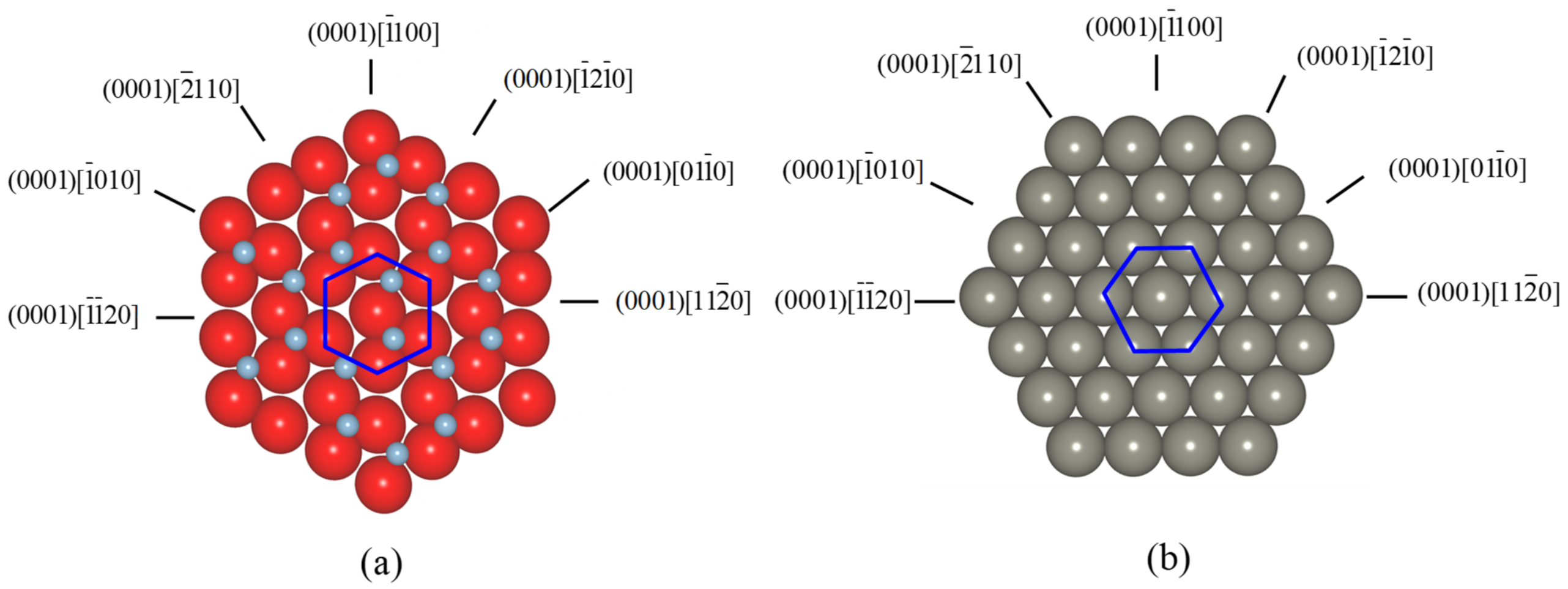
Although single crystal sapphire originally has a rhombohedral structure, it is often approximated by an hcp crystal for convenience. To clearly reveal the anisotropic characteristics of single crystal sapphire, it is essential to display the crystal structure of sapphire. Figure 1 displays the structure of (a) single crystal sapphire compared to (b) Zn which was used in the MD simulation. The crystal structure of sapphire consists of oxygen ions closely packed with aluminum ions embedded in oxygen interstices [18]. According to the Bravais classification of a symmetry crystal, the structure of monocrystalline sapphire belongs to the space group as shown in Figure 1a, and can be described as either a hexagonal or rhombohedral unit cell [19]. On the other hand, Zn with a similar hcp structure [20] belongs to the P63/mmc space group. In Figure 1, it is clear to see the similar hexagonal structure of sapphire and Zn in the basal plane.

2.2. Anisotropic Properties

To illustrate the deformation mechanism of monocrystalline sapphire during nanoscratch, the possible slip/twinning systems and critical shear stresses of sapphire crystal were listed as in Table 1 [14,19,21]. As shown in Table 1, critical shear stress varies with orientation and thus slip or twinning is more likely to occur on the crystal plane where the shear stress exceeds the critical shear stress. Table 2 shows the representative slip/twin systems for Zn [22] for comparison. Comparing Table 1 and Table 2, it can be seen that the basal slip system is totally the same and the primary twinning system is also similar to the rhombohedral and tensile ones, respectively.
Figure 2 shows the top view of basal slip or twinning directions of (a) sapphire and (b) Zn, respectively. The same structure of six-fold symmetry of sapphire and Zn can obviously be seen in the basal plane. According to the critical shear stress shown in Table 1, the possibility of twinning deformation on the rhombohedral plane is relatively high. However, what is the most important is the resolved shear stress exerted on the possible slip/twin systems when a scratching force is applied. It should be noted that in sapphire, basal slip and twinning and prism and pyramidal slips may show 6-fold symmetry, while rhombohedral twinning may show 3-fold symmetry according to the crystal structure.

3. Experimental Set-Up for Nanoscratch

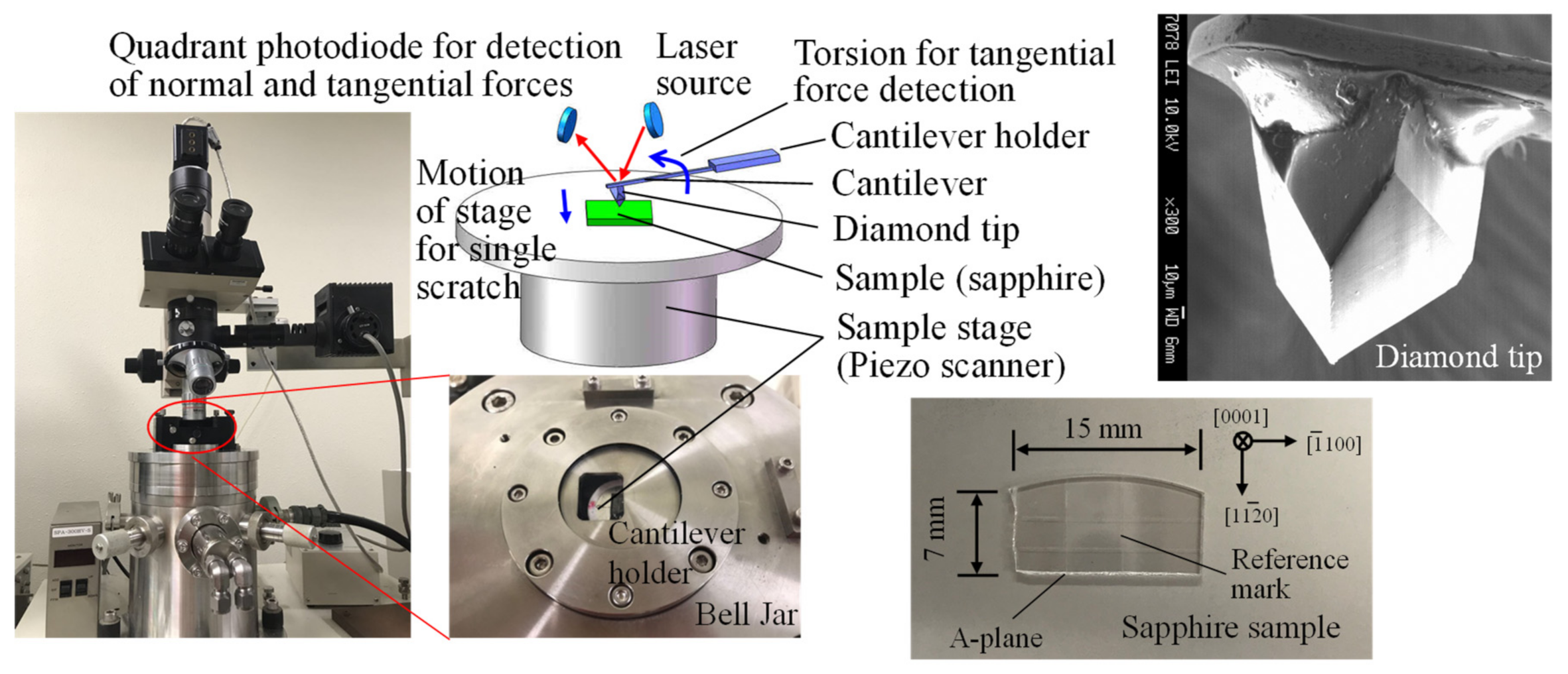
Nanoscratch tests were performed on an SPM (SPA-300HV, Seiko Instruments Co., Japan) with its FFM function using a monocrystalline diamond tip as the scratch tool as shown in Figure 3. During the nanoscratch, a constant normal load was given through bending of a cantilever on which a diamond tip was bonded and monitored and controlled by a piezo scanner/actuator, while the scratch force was monitored using the cantilever’s torsion (torsional displacement). This was detected through a quadrant photodiode considering the torsional stiffness of the cantilever. A 2-inch double-sided polished epi-ready c-plane (0001) sapphire wafer substrate with an A-plane cross-section was cut into a small piece and used as the workpiece as shown in Figure 3.
The scratch directions on the c-plane sapphire are shown in Figure 4. The anisotropy of machinability was investigated by scratching in seven different directions every 30 degrees as shown in Figure 4. The groove geometries were directly measured on the SPM using the same diamond tip used for nanoscratch immediately after each single groove nanoscratch test.

4. Experimental Results

Scratch Force, Depth, and Specific Energy

The nanoscratch experiments were conducted on a c-plane sapphire workpiece. A series of experimental conditions is listed in Table 3.
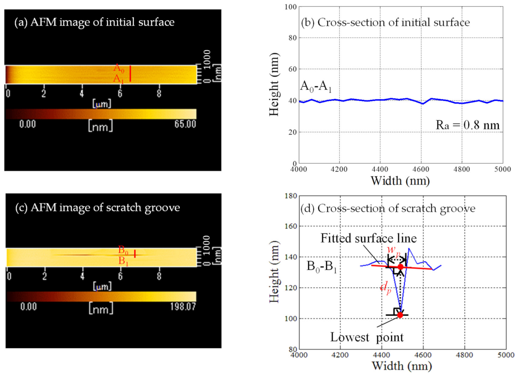
Figure 5 shows AFM images (a) and cross-sections of initial surface (b), scratch groove (c), (d), respectively, where the normal load is 10 µN and the scratch direction is 11 2 ¯ 0   in Figure 5c,d. After each trial, scratch force (tangential force) and depth of scratch grooves were directly measured by the AFM mode of the SPM. Scratch depth and width for each scratch direction was determined using the method shown in Figure 5d and averaged from the results of the five cross-sections.
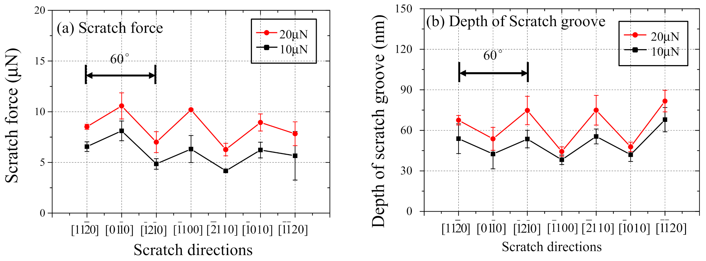
Figure 6 shows the relationship between scratch direction and (a) scratch force and (b) groove depth, respectively. Publications [23,24,25] also reported that the critical depth of cut for sapphire in the ductile-regime was less than 0.24 µm while nanoscratched depths were lower than 85 nm in this study. Therefore, the ductile-regime removal and deformation mechanisms should be discussed in this study, because all the nanoscratch experiments were completed within the ductile-regime.
In Figure 6a, higher scratch forces are obtained when the scratch directions are, 01 1 ¯ 0 , 1 ¯ 100 , and 1 ¯ 010 than those of 11 2 ¯ 0 , 1 ¯ 2 1 ¯ 0 , 2 ¯ 110 , and 11 ¯ 20 . On the contrary, Figure 6b indicates that deeper groove depths are observed when the scratch directions are 11 2 ¯ 0 , 1 ¯ 2 1 ¯ 0 , 2 ¯ 110 , and 11 ¯ 20 than those of 01 1 ¯ 0 , 1 ¯ 100 , and 1 ¯ 010 . According to both figures, the intervals between adjacent peaks or valleys are 60°, such as the 01 1 ¯ 0 and 1 ¯ 100 directions. It illustrates that c-plane sapphire has six-fold symmetrical machinability originating from the atomic arrangements in the basal plane. On the other hand, the rhombohedral planes have three-fold symmetry. Therefore, the influence of the rhombohedral twinning on the deformation would be expected to be small.
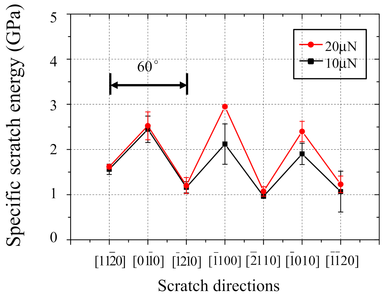
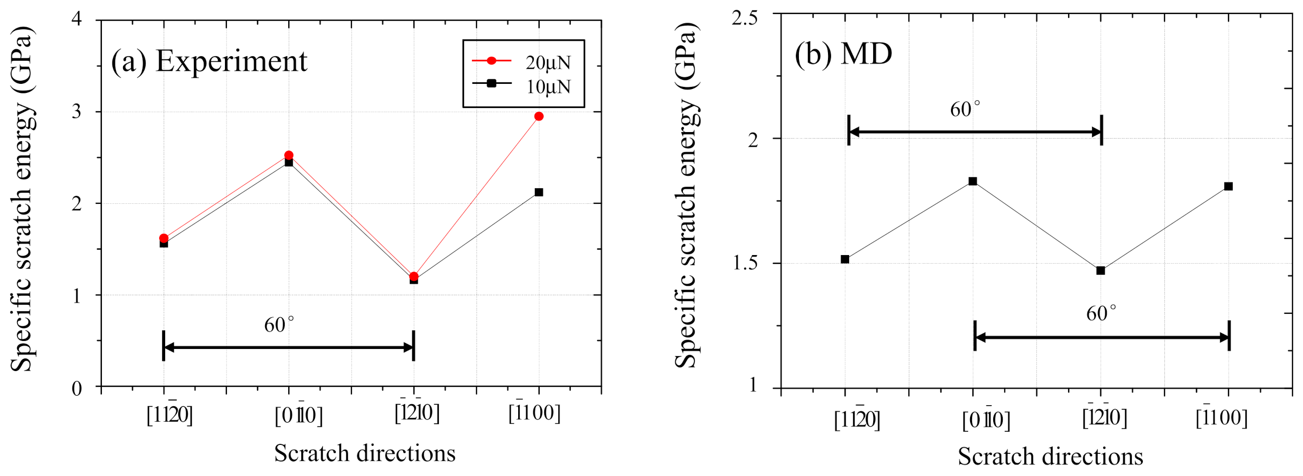
To more accurately grasp the anisotropy in machinability, the relationship between scratch direction and specific scratch energy is shown in Figure 7. The specific scratch energy is calculated considering the cross-sectional shape of the scratch groove (a triangle as shown in Figure 5d) using the following formula:
E = F t L v = 2 F t d p w p
where E is specific scratch energy, Ft is scratch (tangential) force, L is scratch length (5 µm), v is scratched volume, dp is depth of scratch groove, and wp is groove width.
When the scratch directions are 11 2 ¯ 0 , 1 ¯ 2 1 ¯ 0 , 2 ¯ 110 , and 11 ¯ 20 , the lower specific scratch energies are observed. The specific scratch energies are around 1 GPa which is far less than those of the 01 1 ¯ 0 , 1 ¯ 100 , and 1 ¯ 010 directions. The specific scratch energy clearly shows six-fold symmetry as seen in Figure 6a,b. It also revealed that the basal plane played an essential role in the material deformation of sapphire being different from the prism, pyramidal, and rhombohedral planes when single groove nanoscratch is performed on c-plane sapphire. Furthermore, it also implied that the lower specific scratch energies were observed along the basal slip directions, and it indicates higher possibility of basal slip to occur than that of basal twinning.

5. Molecular Dynamics Modeling for Hcp Crystal

The MD simulation is visualized and an effective method for understanding the material removal and deformation mechanisms in nanoscale machining processes [26,27]. In order to reveal that the deformation on the basal plane plays an essential role for the hcp crystal when nanoscratch tests are conducted on c-plane substrate, in this study, MD simulations of Zn, one of the simple hcp crystals, were performed to basically understand the fundamental removal and deformation mechanisms, since sapphire has a more complicated atomic structure than Zn.
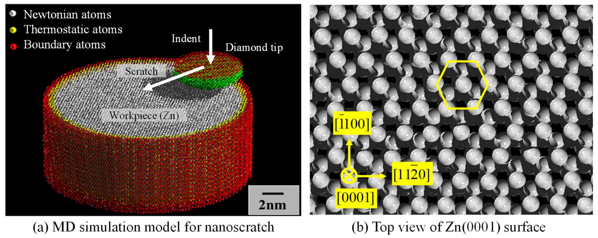
The self-developed MD simulation model for nanoscratch tests is shown in Figure 8a. The workpiece and the tool tip are assumed to consist of monocrystalline Zn and diamond (C), respectively. In the MD simulation [28], by taking the mass of atom i to be mi, its position at time t to be Ri(t), and the resultant force obtained by summing up the interactions from all the neighboring atoms to be Fi(t), the following equation of motion of Newton’s second law is obtained:
m i d 2 R i t d t 2 = F i t
The interatomic forces can be calculated from the gradient of the interatomic potential functions explained later. Equation (2) is applied to all the atoms of interest and solved using the leap-frog method [29] and solved individually at each time step, where the time step is 2 fs. In the present trials, Morse potential functions were used for Zn–Zn [30] and Zn–C interactions with the parameters shown in Table 4, respectively. If emphasis is placed on the characterization of Zn, an EAM (embedded-atom method) potential [31] should be used. However, since the comparison target in this paper is sapphire, a hard and brittle material, for the purpose of investigating the similarity in the deformation with hcp crystals, a Morse potential, that tends to underestimate the ductility, was used between a pair of Zn–Zn atoms.
Morse potential function is as follows:
r i j = D exp 2 α r i j r 0 2 exp α r i j r 0
where is the potential energy, rij is the interatomic distance between i and j atoms, D is the dissociation (cohesion) energy, r0 is the equilibrium bond length, and α is the potential coefficient, respectively.
Since the potential parameters between Zn and C are unknown, they were estimated using the mixing law [32], and D was reduced to 1/10 to prevent non-physical phenomena due to extremely strong adhesion between the workpiece and the diamond tip. It was considered more realistic to treat it as such in the case of the actual scratching events in the atmosphere. The cut off distance was set to 3a here.
The Tersoff potential function [33], which is one of the most popular multibody interatomic potentials for diamond, can be applied to the interactions among C atoms of the diamond tip [34,35]. Generally, the total energy Es of the system in the form of the Tersoff potential is as follows:
E s = 1 2 i j i f C r i j a i j f R r i j + b i j f A r i j
where f C r i j is the cutoff function, f R r i j is the repulsive force term, f A r i j is the attractive force term, b i j is the multi-body force term and a i j is taken as 1, generally.
For simplification, all the trials were performed in vacuum, and no chemical reactions were considered. The workpiece was assumed to have a free, completely clean and ideal Zn(0001) structure in its uppermost surface as shown in Figure 8b. Other than the up-permost surface of Zn was surrounded by a thermostat layer (Nose-Hoover thermostat using the velocity scaling method to keep temperature constant [29]) where atoms are arrayed in a lattice constant length a of Zn. The mechanical energies increased in the analysis area due to the plastic deformations by scratching being able to be dissipated from this thermostat layer. The area outside the thermostat layer was assumed to be a perfect rigid body. The diamond tip was also composed of the analysis area, thermostat, and perfect rigid body layers. Such a model is often used in the MD simulation of machining processes. A cylindrical workpiece is used because a cubic workpiece is not suitable for investigating the anisotropy of machinability. Since the depths of the scratch grooves were smaller than the diamond tip radius in the experiment, the shape of the tip was assumed to be hemispherical in the simulation as well. Due to the limited size of the model, it was difficult to completely eliminate the effect of the boundaries on the deformation. Nevertheless, the developed model was large enough to analyze the machining anisotropy due to crystal anisotropy.
In the preparation of the initial MD model, considering the principle of minimum potential energy, atomic arrays of Zn and diamond were obtained at absolute zero temperature, then the atomic arrays at 300 K for the workpiece and diamond tip were arranged considering the thermal expansion, and mean-velocity vectors at 300 K, randomly given to all atoms. Next, Newton’s motion-equations were solved and velocity scaling was implemented sequentially until the system became stable, when the analysis area and the thermostat layer were calculated separately. As a result, atomic array models with surfaces were constructed. It was also confirmed that the velocity of the atoms followed Maxwell distributions. These results confirmed the validity of the initial array models. At this stage, we had an MD simulation of the microcanonical ensemble, where the number of atoms, temperature, and energy were both constant. On the other hand, after the motion of the diamond tip has started, it is a non-equilibrium MD simulation, where the number of atoms is constant and only the temperature of the thermostat is constant (300 K).

6. MD Simulation Results and Discussion

6.1. MD Simulation Results

The series of the simulation conditions is listed in Table 5. A diamond tip was slid horizontally onto the surface of the workpiece at a constant speed of 20 m/s by giving a displacement equivalent to 20 m/s at each time step after indenting it into the Zn(0001) surface to a depth of 1.3 nm. The scratch directions were chosen referencing those of the experiments. Although 20 m/s is remarkably faster than that of the experiment, it is slow enough compared to the speed of elastic and plastic waves, and it can be a reasonable speed to evaluate the plastic deformations of the crystal. Also, the results of scratching at the speed lower than single digits were almost identical. Since constant load control may lead to vibration of the diamond tip, for stability, simulations with a constant depth of cut were attempted, being different from the experiments.
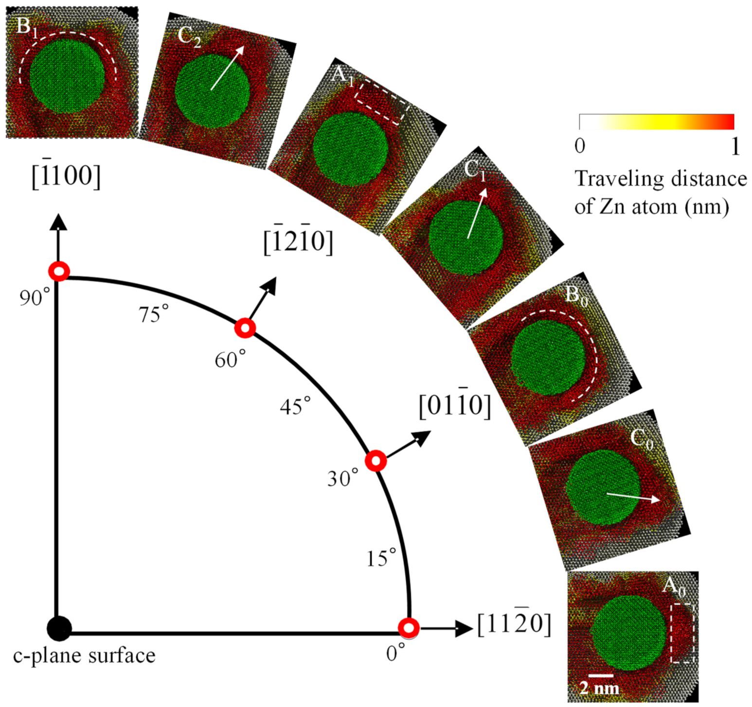
Figure 9 shows the snapshots of the cross-section for various scratch directions, where each cross-section is parallel to the scratch direction of interest. In Figure 9, (a) to (g) show the results when the 11 2 ¯ 0 direction is set to be (a) 0 degree and the scratch direction is tilted every 15 degrees in the counterclockwise direction, and (h) shows the schematic of the scratch directions. In the case of (a) 11 2 ¯ 0 (0 deg.) and (e) 2 11 ¯ 0 (60 deg.) directions, short cutting chips are generated, respectively, and remarkably similar forms of deformation can be observed. The Zn atoms surrounded by the square beneath the diamond tip slide horizontally to the left, such as along 0001 11 2 ¯ 0 and 0001 1 ¯ 2 1 ¯ 0 ,   and cause basal slip deformations. The basal slips change their directions diagonally upward at the region diagonally below and forward of the diamond tip as circled by the ellipse in Figure 9e. This plays a major role for the formation of the shear planes in a cutting chip. In particular, basal slip is important in promoting chip generation because its deformation capacity is larger than that of twinning. From Figure 9e, it can be seen that the deformation diagonally upward after the basal slip is complicated with a mixture of pyramidal slips <c+a> along 1 ¯ 2 1 ¯ 3 1 2 ¯ 12   and partial dislocations. This is considered to be less deformable than the pure slip represented by the basal one. In the case of sapphire, the effects of pyramidal slip, rhombohedral twinning, and partial dislocations are expected to be mixed in a complex manner.
On the other hand, in the case of (c) 10 1 ¯ 0 (30 deg.) and (g) 1 ¯ 100 (90 deg.), they are limited to occurrence of wedge-formation type ploughing rather than the formation of short cutting chips. The deformations of (c) and (g) are also similar. From Figure 9e, it can be observed that the region surrounded by a square has a different crystal arrangement from the deeper parts (see the solid lines). This is due to the compression twin along 0 1 ¯ 11 01 1 ¯ 2 based on partial dislocations. A kind of partial dislocation is also found in the region shown by the ellipse in Figure 9g. In the case of sapphire, basal twinning is expected to occur.
In the case of intermediate (b) 15 deg., (d) 45 deg. and (f) 75 deg., it can be seen that the chip formation heights are intermediate of the former different two groups.
Figure 10 is the result of displaying the top views in all the scratch directions to observe the chip formation morphologies. From the result, it can be observed that the cutting chips are smoothly generated forward when scratched in the basal slip direction (see, rectangles of A0 and A1). On the other hand, it can be observed that burrs are likely to occur in the lateral direction when scratched in the 30 and 90 degrees directions (see, half circles of B0 and B1). These trends are almost the same as that of the MD simulation results obtained by Lin, et al. [17]. Furthermore, it can be also observed when scratched in the 15, 45 and 75 deg. directions, the cutting chips are generated tilting toward the basal slip directions (see, arrows of C0, C1, and C2). These results also clearly show that the basal slip is highly deformable.
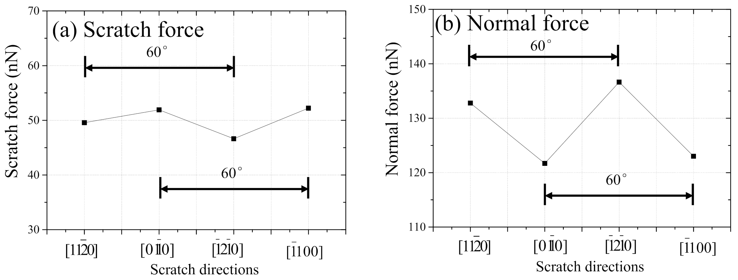
Figure 11 shows the relationship between scratch direction and (a) scratch force and (b) normal force, respectively. Both forces were average values from the start to a scratch distance of 8 nm. In Figure 11a, higher scratch forces are obtained when the scratch directions are 01 1 ¯ 0 and 1 ¯ 100 than those of 11 2 ¯ 0 and 1 ¯ 2 1 ¯ 0 . This trend is the same as that of the experimental results shown in Figure 6a. On the contrary, Figure 11b indicates that higher normal forces are observed when the scratch directions are 11 2 ¯ 0 and 1 ¯ 2 1 ¯ 0 than those of 01 1 ¯ 0 and 1 ¯ 100 . Higher loads lead to higher hardness or smaller plasticity. This indicates that extra or undesired plastic deformation is unlikely to occur when the scratch directions are 11 2 ¯ 0 and 1 ¯ 2 1 ¯ 0 . In both figures, the intervals between adjacent peaks or valleys are 60°. This illustrates that Zn(0001) has a six-fold symmetrical machinability originating from the atomic arrangements in the basal plane just as observed in the aforementioned experimental results of the c-plane sapphire.

6.2. Comparison between Experimental and Simulation Results

Figure 12 show the comparison between experimental ((a) 10 µN and (b) 20 µN) and (c) MD simulation results regarding the effect of scratching direction on burr height. In the experimental results shown in Figure 12a,b, the heights of the burrs on the left and right are remarkably different although the apex of the diamond tip is rounded. It is because the diamond tip is a triangular pyramid that side-forward nanoscratch tests were performed in the first place. Even so, it can be confirmed that the burr heights become lower, when the scratch tests are conducted in the direction of basal slip such as 11 2 ¯ 0 and 1 ¯ 2 1 ¯ 0 . An identical trend can be confirmed in the MD simulation result as well, as shown in Figure 12c.
Figure 13 shows the comparison between (a) simulation and (b) experimental results regarding the effect of scratching direction on specific scratch energy. The removal volume in the MD simulation was obtained from the number of Zn atoms moved over one Burgers vector of Zn, and it showed a similar trend to that of the groove depth shown in Figure 6b although not shown here. The specific scratch energy was calculated using a similar method as Equation (1). From the experimental results shown in Figure 13a, when scratched in the direction of basal slip such as 11 2 ¯ 0 and 1 ¯ 2 1 ¯ 0 , the specific scratch energies become remarkably lower than those of 01 1 ¯ 0 and 1 ¯ 100 . An identical trend can obviously be confirmed from the MD simulation result shown in Figure 13b as well.
These results clearly show that the machining efficiency is maximized and the accuracy can be improved by scratching in the basal slip direction. This is due to the larger deformability of basal slip than that of twinning, which would lead to smooth and effective cutting chip formation.

7. Conclusions

Single groove nanoscratch experiments were conducted on c-plane sapphire wafer to analyze the ductile-regime removal and deformation mechanism including the anisotropy. As a result, the specific scratch energy showed a trend of six-fold symmetry which was thought to be due to basal slip or twinning. To clarify the nanoscratch mechanism, particularly the anisotropy, an MD simulation of Zn, which is one of the hcp crystals with similar slip/twin systems, was performed. From the comparison between the experimental and the MD simulation results regarding the effect of scratching direction on specific scratch energy and burr height, it was found that in the single groove nanoscratch, the specific scratch energy and the burr height are minimized, and the machining efficiency is maximized while the accuracy can be improved by scratching along the basal slip direction. This is due to the larger deformability of basal slip leading to smooth and effective cutting chip formation.

Author Contributions

Conceptualization, W.L., J.S., L.Z. and T.O.; experiments, W.L.; simulations, W.L and N.Y.; supervision, J.S., L.Z., T.O. and H.O.; writing original draft, W.L., N.Y., J.S., L.Z., T.O. and H.O.; funding acquisition, L.Z. and J.S. All authors have read and agreed to the published version of the manuscript.

Funding

This work is partially supported by JSPS KAKENHI, Grant Number 15H02213 and 20K04235.

Data Availability Statement

Not applicable.

Conflicts of Interest

The authors declare no conflict of interest.

References

  1. Khattak, C.P.; Shetty, R.; Schwerdtfeger, C.R.; Ullal, S. World’s largest sapphire for many applications. J. Cryst. Growth 2016, 452, 44–48. [Google Scholar] [CrossRef]
  2. Shang, L.; Xu, B.; Ma, S.; Liu, Q.; Ouyang, H.; Shan, H.; Hao, X.; Han, B. The Surface Morphology Evolution of GaN Nucleation Layer during Annealing and Its Influence on the Crystal Quality of GaN Films. Coatings 2021, 11, 188. [Google Scholar] [CrossRef]
  3. Wang, Q.; Liang, Z.; Wang, X.; Zhao, W.; Wu, Y.; Zhou, T. Fractal analysis of surface topography in ground monocrystal sapphire. Appl. Surf. Sci. 2015, 327, 182–189. [Google Scholar] [CrossRef]
  4. Soltis, P.J. Anisotropic Mechanical Behavior in Sapphire (Al2O3) Whiskers; Naval Air Engineering Center Lakehurst NJ Aeronautical Materials Lab, Defense Technical Information Center: Fort Belvoir, VA, USA, 1964. [Google Scholar]
  5. Wiederhorn, S.M. Fracture of sapphire. J. Am. Ceram. Soc. 1969, 52, 485–491. [Google Scholar] [CrossRef]
  6. Nowak, R.; Sekino, T.; Niihara, K. Surface deformation of sapphire crystal. Philos. Mag. A 1996, 74, 171–194. [Google Scholar] [CrossRef]
  7. Voloshin, A.V.; Dolzhenkova, E.F.; Litvinov, L.A. Anisotropy of deformation and fracture processes in sapphire surface. J. Superhard Mat. 2015, 37, 341–345. [Google Scholar] [CrossRef]
  8. Hockey, B.J. Plastic deformation of aluminum oxide by indentation and abrasion. J. Am. Ceram. Soc. 1971, 54, 223–231. [Google Scholar] [CrossRef]
  9. Chan, H.M.; Lawn, B.R. Indentation deformation and fracture of sapphire. J. Am. Ceram. Soc. 1988, 71, 29–35. [Google Scholar] [CrossRef]
  10. Lin, J.; Jiang, F.; Xu, X.; Jing, L.; Tian, Z.; Wen, Q.; Lu, X. Molecular dynamics simulation of nanoindentation on c-plane sapphire. Mech. Mater. 2021, 154, 103716. [Google Scholar] [CrossRef]
  11. Pöhl, F.; Hardes, C.; Theisen, W. Scratch behavior of soft metallic materials. AIMS Mater. Sci. 2016, 3, 390–403. [Google Scholar] [CrossRef]
  12. Wang, J.; Guo, B.; Zhao, Q.; Zhang, C.; Zhang, Q.; Chen, H.; Sun, J. Dependence of material removal on crystal orientation of sapphire under cross scratching. J. Eur. Ceram. Soc. 2017, 37, 2465–2472. [Google Scholar] [CrossRef]
  13. Mizumoto, Y.; Maas, P.; Kakinuma, Y.; Min, S. Investigation of the cutting mechanisms and the anisotropic ductility of monocrystalline sapphire. CIRP Ann. 2017, 66, 89–92. [Google Scholar] [CrossRef]
  14. Kareer, A.; Tarleton, E.; Hardie, C.; Hainsworth, S.V.; Wilkinson, A.J. Scratching the surface: Elastic rotations beneath nanoscratch and nanoindentation tests. Acta Met. 2020, 200, 116–126. [Google Scholar] [CrossRef]
  15. Lee, S.H. Analysis of ductile mode and brittle transition of AFM nanomachining of silicon. Int. J. Mach. Tools and Manuf. 2012, 61, 71–79. [Google Scholar] [CrossRef]
  16. Abdelkawy, A.; Yoshino, M.; Nakagawa, Y. Effect of Tool Rake Angle and Crystal Orientation on Ductile Mode Cutting of Hard/Brittle Materials. Int. J. Automation Technol. 2020, 14, 253–259. [Google Scholar] [CrossRef]
  17. Lin, J.; Jiang, F.; Wen, Q.; Wu, Y.; Lu, J.; Tian, Z.; Wang, N. Deformation anisotropy of nano-scratching on C-plane of sapphire: A molecular dynamics study and experiment. Appl. Surf. Sci. 2021, 546, 149091. [Google Scholar] [CrossRef]
  18. Heid, R.; Strauch, D.; Bohnen, K.P. Ab initio lattice dynamics of sapphire. Phys. Rev. B 2000, 61, 8625–8627. [Google Scholar] [CrossRef]
  19. Dobrovinskaya, E.R.; Lytvynov, L.A.; Pishchik, V. Sapphire: Material, Manufacturing, Application; Springer Science & Business Media: New York, NY, USA, 2009. [Google Scholar]
  20. Ganeshan, S.; Hector Jr, L.G.; Liu, Z.K. First-principles study of self-diffusion in hcp Mg and Zn. Comput. Mat. Sci. 2010, 50, 301–307. [Google Scholar] [CrossRef]
  21. Clayton, J.D. A continuum description of nonlinear elasticity slip and twinning, with application to sapphire. Proc. Roy. Soc. A 2009, 465, 307–334. [Google Scholar] [CrossRef]
  22. Yoo, M.H. Slip, twinning, and fracture in hexagonal close-packed metals. Metall. Trans. A 1981, 12, 409–418. [Google Scholar] [CrossRef]
  23. Maas, P.; Mizumoto, Y.; Kakinuma, Y.; Min, S. Anisotropic brittle-ductile transition of monocrystalline sapphire during orthogonal cutting and nanoindentation experiments. Nanotech. Prec. Eng. 2018, 1, 157–171. [Google Scholar] [CrossRef]
  24. Mohammadi, H.; Patten, J.A. Anisotropy Effect on Cutting Monocrystal Sapphire by Micro-Laser Assisted Machining Technique. In Proceedings of the ASME 2016 11th International Manufacturing Science and Engineering Conference, Blacksburg, VA, USA, 27 June–1 July 2016. [Google Scholar]
  25. Wang, J.; Guo, B.; Zhao, Q.; Zhang, C.; Zhang, Q.; Zhai, W. Evolution of material removal modes of sapphire under varied scratching depths. Ceram. Int. 2017, 43, 10353–10360. [Google Scholar] [CrossRef]
  26. Li, J.; Fang, Q.; Liu, Y.; Zhang, L. A molecular dynamics investigation into the mechanisms of subsurface damage and material removal of monocrystalline copper subjected to nanoscale high speed grinding. Appl. Surf. Sci. 2014, 303, 331–343. [Google Scholar] [CrossRef]
  27. Yan, Y.; Sun, T.; Dong, S.; Liang, Y. Study on effects of the feed on AFM-based nano-scratching process using MD simulation. Comput. Mater. Sci. 2007, 40, 1–5. [Google Scholar] [CrossRef]
  28. Hoover, W.G. Molecular Dynamics; Springer: Berlin, Germany, 1986. [Google Scholar]
  29. Hockney, R.W. The potential calculation and some applications. Methods Comput. Phys. 1970, 9, 135–211. [Google Scholar]
  30. Hung, N.V. A Method for Calculation of Morse Potential for fcc, bcc, hcp Crystals Applied to Debye-Waller Factor and Equation of State. Commun. Phys. 2004, 14, 7–14. [Google Scholar] [CrossRef]
  31. Daw, M.S.; Baskes, M.I. Embedded-atom method: Derivation and application to impurities, surfaces, and other defects in metals. Phys. Rev. B 1984, 29, 6443–6453. [Google Scholar] [CrossRef] [Green Version]
  32. Imafuku, M.; Sasajima, Y.; Yamamoto, R.; Doyama, M. Computer simulations of the structures of the metallic superlattices Au/Ni and Cu/Ni and their elastic moduli. J. Phys. F Met. Phys. 1986, 16, 823–830. [Google Scholar] [CrossRef]
  33. Tersoff, J. Empirical interatomic potential for carbon, with applications to amorphous carbon. Phys. Rev. Lett. 1988, 61, 2879–2882. [Google Scholar] [CrossRef] [Green Version]
  34. Shimizu, J.; Eda, H.; Zhou, L.; Okabe, H. Molecular Dynamics Simulation of Adhesion Effect on Material Removal and Tool Wear in Diamond Grinding of Silicon Wafer. Tribol. Online 2008, 3, 248–253. [Google Scholar] [CrossRef] [Green Version]
  35. Shimizu, J.; Zhou, L.; Yamamoto, T. Molecular Dynamics Simulation of Chemical Reaction Assisted Grinding of Silicon Wafer by Controlling Interatomic Potential Parameters. J. Comput. Theor. Nanosci. 2010, 7, 2165–2170. [Google Scholar] [CrossRef]
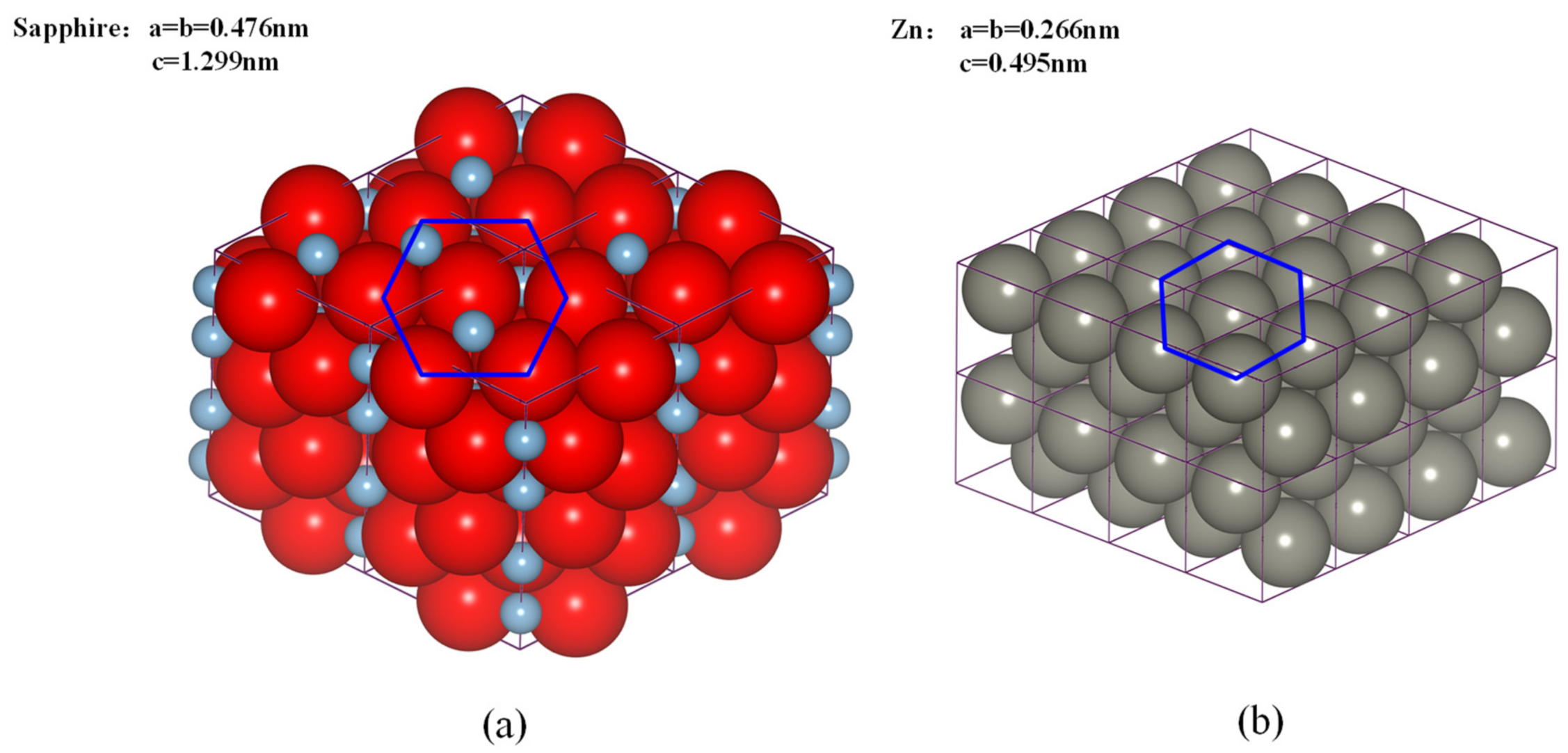
Figure 1. Schematic of the crystal arrangement of (a) sapphire (blue and red balls represent Al3+ and O2− ions, respectively.) and (b) Zn, respectively.
Nanomaterials 11 01739 g001
Figure 2. Top view of basal slip or twinning directions of (a) sapphire and (b) Zn.
Nanomaterials 11 01739 g002
Figure 3. Appearance of SPM and schematic of nanoscratching model using FFM mode with the images of sapphire sample and diamond tip.
Nanomaterials 11 01739 g003
Figure 4. Schematic of defined nanoscratch directions on c-plane sapphire.
Nanomaterials 11 01739 g004
Figure 5. AFM images and cross-sections of initial surface (a,b) and scratch groove (c,d), respectively.
Nanomaterials 11 01739 g005
Figure 6. The relationship between scratch direction and (a) scratch force and (b) depth of scratch groove, respectively.
Nanomaterials 11 01739 g006
Figure 7. The relationship between scratch direction and specific scratch energy.
Nanomaterials 11 01739 g007
Figure 8. (a) MD simulation model for nanoscratch and (b) top view of Zn(0001) surface.
Nanomaterials 11 01739 g008
Figure 9. Snapshots of the cross-section for various scratch directions such as (a) 0, (b) 15, (c) 30, (d) 45, (e) 60, (f) 75 and (g) 90 degrees from 11 2 ¯ 0 , where the color bar shows the traveling distance of Zn atom from initial position, and (h) is the schematic for scratch directions (MD).
Nanomaterials 11 01739 g009
Figure 10. Top views in all the scratch directions to observe the chip formation morphologies, where the color bar shows the traveling distance of Zn atom from initial position (MD).
Nanomaterials 11 01739 g010
Figure 11. The relationship between scratch direction and (a) scratch force and (b) normal force, respectively (MD).
Nanomaterials 11 01739 g011
Figure 12. Comparison between experimental ((a) 10 μN, (b) 20 μN) and (c) MD simulation results regarding the effect of scratching direction on burr height.
Nanomaterials 11 01739 g012
Figure 13. Comparison between (a) experimental and (b) simulation results regarding the effect of scratching direction on specific scratch energy.
Nanomaterials 11 01739 g013
Table 1. Slip/twinning systems and critical shear stresses for sapphire [14,19,21].
Slip/Twinning SystemDescription Critical   Shear   Stress   τ c ( GPa )
0001 11 2 ¯ 0 Basal slip2.7 < τ c  < 5.0
0001 1 ¯ 010 Basal twinning τ c  > 4.0
11 2 ¯ 0 1 ¯ 100 Prism slip2.3 < τ c  < 5.7
0 1 ¯ 11 10 1 ¯ 1 Pyramidal slip τ c  > 7.0
1 ¯ 012 10 1 ¯ 1 Rhombohedral twinning1.0 < τ c  < 8.1
Table 2. Representative slip/twin systems for zinc [22].
Slip/Twin SystemDescription
0001 11 2 ¯ 0 Basal slip
1 1 ¯ 00 11 2 ¯ 0 Prismatic slip
1 1 ¯ 01 11 2 ¯ 0 Pyramidal slip <a>
11 2 ¯ 2 11 ¯ 23 Pyramidal slip <c+a>
10 1 ¯ 2 1 ¯ 011 Tensile twin
10 1 ¯ 1 1 ¯ 012 Compression twin
Table 3. Experimental conditions for the single groove nanoscratch test.
InstrumentSPM (SPA-300HV, Seiko Instruments Co., Japan)
WorkpieceSapphire (c-plane)
Diamond tipTrigonal pyramid (Tip radius = 100 nm)
Cantilever stiffness (N/m)200
Normal load for observation (µN)0.2
Normal load for nanoscratch test (µN)10, 20
Scratch direction 11 2 ¯ 0 , 10 1 ¯ 0 , 2 11 ¯ 0 , 1 ¯ 100 , 1 2 ¯ 10 , 0 1 ¯ 10 , 11 ¯ 20
Scratch speed (µm/s)16
Scratch length (µm)5
Table 4. Morse potential parameters.
ParameterZn-Zn [30]C-Zn
D (eV)0.17000.06418
α  (Å)1.7052.13
r 0  (Å−1)2.7932.6363
Table 5. Conditions for MD simulation of single groove nanoscratch.
WorkpieceMonocrystalline Zinc (Zn(0001))
Dimension of analysis area of workpiece (nm)Radius: 8.1, Height: 6.7
Scratching tool tipMonocrystalline diamond (C)
Dimension of analysis area of tool tip (nm)Tip radius: 4.5, Height: 2.2
Initial and thermostat temperatures (K)300
Scratch depth (nm)1.3
Scratch length (nm)8
Scratch speed (m/s)20
Scratch direction 11 2 ¯ 0 , 10 1 ¯ 0 , 2 11 ¯ 0 , 1 ¯ 100
Publisher’s Note: MDPI stays neutral with regard to jurisdictional claims in published maps and institutional affiliations.