Abstract
Anisotropic materials provide a new platform for building diverse polarization-dependent optical devices. Two-dimensional α-phase molybdenum trioxides (α-MoO3), as newly emerging natural van der Waals materials, have attracted significant attention due to their unique anisotropy. In this work, we theoretically propose an anisotropic perfect metamaterial absorber in visible frequencies, the unit cell of which consists of a multi-layered α-MoO3 nanoribbon/dielectric structure stacked on a silver substrate. Additionally, the number of perfect absorption bands is closely related to the α-MoO3 nanoribbon/dielectric layers. When the proposed absorber is composed of three α-MoO3 nanoribbon/dielectric layers, electromagnetic simulations show that triple-band perfect absorption can be achieved for polarization along [100], and [001] in the direction of, α-MoO3, respectively. Moreover, the calculation results obtained by the finite-difference time-domain (FDTD) method are consistent with the effective impedance of the designed absorber. The physical mechanism of multi-band perfect absorption can be attributed to resonant grating modes and the interference effect of Fabry–Pérot cavity modes. In addition, the absorption spectra of the proposed structure, as a function of wavelength and the related geometrical parameters, have been calculated and analyzed in detail. Our proposed absorber may have potential applications in spectral imaging, photo-detectors, sensors, etc.
1. Introduction
Two-dimensional (2D) materials with weak van der Waals (vdW) interaction between atomic layers have drawn wide attention due to their extraordinary physical, chemical, and optoelectronic properties, such as graphene [1], hexagonal boron nitride (h-BN) [2,3], transition metal dichalcogenides (TMDs) [4], and black phosphorus (BP) [5,6,7,8]. By breaking the vdW bonds, monolayer 2D materials can be achieved and further transferred to the desired substrates [9,10,11]. In recent years, it has been demonstrated, both theoretically and experimentally, that plasmons can support low propagation loss and strong field confinement in a few or even monolayer 2D materials. Additionally, the spectral responses in these 2D materials can be dynamically tuned by chemical doping or electrical bias. Recently, a new type of 2D vdW semiconducting crystal, α-phase molybdenum trioxide (α-MoO3), has intrigued many researchers due to its highly anisotropic properties [12]. The strong anisotropy, originating from the unique crystalline structure of α-MoO3, can lead to previously reported naturally occurring in-plane hyperbolicity that is associated with the distinct lattice modes along three orthogonal crystal directions. In contrast to the monoclinic and hexagonal phase of crystal MoO3, orthorhombic MoO3 (α-phase) is more thermodynamically stable, which is constituted by planar layered sheets of linked and distorted MoO6 octahedra. Therefore, the newly emerging α-MoO3 materials can be integrated into metamaterials to achieve more freedom in controlling light–matter interactions. Moreover, it provides a new opportunity in the applications of polarization angle-dependent photonic devices, including polarization reflectors and polarization color filters [13]. In addition, some other novel physical phenomena and applications were found based on α-phase molybdenum trioxide. For instance, Hu et al. observed the topological polaritons and photonic magic angle in twisted α-MoO3 bi-layers [14]. Dereshgi et al. proposed lithography-free IR polarization converters via orthogonal in-plane phonons in α-MoO3 flakes [15].
As an important application in metamaterials, a perfect absorber [16,17,18,19,20], which is constructed by metal to achieve resonant coupling with incident electromagnetics, was first proposed by Landy et al. [21]. Since then, narrow-band absorption [22,23], broadband absorption [24,25], chiral-selective absorption [26], polarization-independent and angle-insensitive tunable absorption [27], and even multi-band metamaterial absorbers [28,29] have been extensively studied and applied in plasmonic light harvesting [30], polarization detectors [31], solar energy [27], and infrared cloaking [32]. In recent years, a variety of 2D-materials-based metamaterials have been proposed for achieving tunable enhancing optical absorbance and perfect absorption. For example, Luo et al. theoretically proposed a tunable narrowband absorber based on graphene film and realized an ultra-narrowband perfect absorption peak [33]. Zhu et al. theoretically proposed a tunable ultra-broadband and wide-angle perfect absorber based on stacked monolayer black phosphorus nanoribbons and black phosphorus–dielectric–metallic hybrid architecture [34,35], respectively. Sang et al. presented a dual-band absorber based on monolayer molybdenum disulfide (MoS2) [36]. Recently, Deng et al. presented a broadband absorber with an in-plane trapezoid α-MoO3 patch arrays structure in an infrared regime [37]. Dong et al. proposed an absorber with a single resonant peak by utilizing α-MoO3 combined with a dielectric distributed Bragg reflector in a mid-infrared frequency [38]. However, the potential of α-MoO3 materials in metamaterial absorbers has been underutilized. In particular, to our knowledge, an α-MoO3-based perfect absorber with multiband in the visible frequency regime has not yet been reported. Our effort in this work is directed toward extending single-band perfect absorption to triple-band absorption, which is of great importance for wide applications, such as spectral imaging, photodetectors, sensors, etc.
In this work, we theoretically and numerically propose an anisotropic metamaterial absorber which is composed of multiple α-MoO3/dielectric layers stacked on a silver mirror. Triple-band perfect absorption can be achieved in visible frequencies for both polarizations along x- and y-directions, respectively. The highly anisotropy results from the anisotropic lattice structure and the polarization-dependent complex refractive index of α-MoO3. Additionally, the operation mechanism of perfect absorption can be explained by the resonant grating modes and the interference effect of Fabry–Pérot cavity modes. Moreover, simulation results obtained by the finite-difference time-domain (FDTD) method are consistent with the theoretical analysis of impedance match. In addition, the absorption spectra of the proposed structure, as a function of wavelength and the related geometrical parameters, have been calculated and analyzed in detail.
2. Materials and Methods
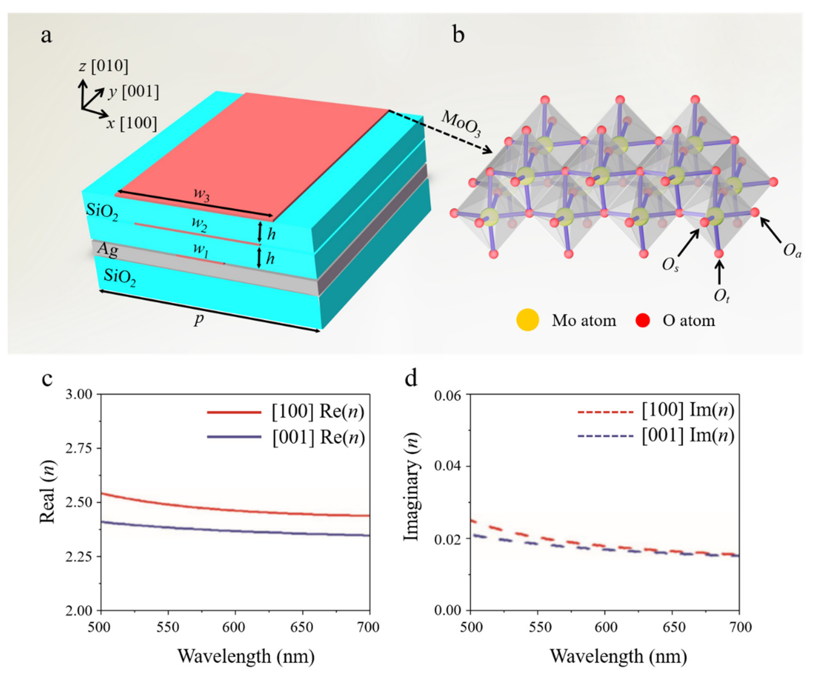
Figure 1a schematically shows the unit cell of the proposed perfect absorber consisting of alternating layers of α-MoO3 nanoribbon and dielectrics stacked on a silver mirror. The related geometrical parameters and their corresponding values are given in the caption of Figure 1. In the design, the crystal directions [100], [001], and [010] refer to x-, y-, and z-directions in the rectangular coordinate system, separately. Figure 1b illustrates the orthorhombic α-MoO3 structure, which has three different types of oxygen atom, i.e., terminal Ot along [010] direction bonded with a Mo atom, asymmetric Oa along [100] direction bonded with two Mo atoms, and symmetrical Os along [001] direction bonded with three Mo atoms. In general, the special atomic structure highly influences the properties of α-MoO3, resulting in unique optical anisotropy. Here, we use complex dielectric function to describe its optical properties [13]:
where , j indicates the total number of oscillators, ε∞, ωpj, ωoj, and γj refer to the high frequency dielectric constant, the plasma frequency, the eigenfrequency, and the scattering rate of the jth Lorentz oscillator, respectively. The above parameters used in Equation (1) are given in Table 1. Figure 1c,d shows the real and imaginary part of the complex refractive index of α-MoO3 in the visible region. Compared with the other 2D materials, such as graphene and BP, the complex refractive index of α-MoO3 exhibits a good trade-off between high index and low loss.

Figure 1.
(a) The schematic diagram of the unit of proposed absorber, consisting of multilayer α-MoO3 nanoribbons/SiO2 stacked on a silver substrate. In this design, the optimized geometrical parameters are listed as follows: h = 100 nm, w1 = 105 nm, w2 = 275 nm, w3 = 345 nm, p = 500 nm. (b) The layered orthorhombic α-MoO3 structure, in which the yellow and red balls represent molybdenum and oxygen atoms, respectively. Real (c) and imaginary (d) parts of the refractive index of α-MoO3 in the visible region.

Table 1.
Parameters used in Equation (1) to obtain the permittivity tensors of α-MoO3 in the visible range.
In simulations, the thickness of α-MoO3 was assumed to be 10 nm. The full-field electromagnetic wave calculations were performed by a three-dimensional FDTD method. Additionally, the light waves were incident from the top side along the negative z-direction, and periodic boundary conditions were applied in x- and y- directions. The spectral absorption is calculated by A = 1 − R − T, where R and T represent the reflection and transmission, respectively. Considering the existence of thick silver layer (200 nm), the transmission T is zero. Therefore, the absorption can be simplified by A = 1 − R. In addition, impedance of the proposed structure should match with that of normalized impedance in free space (Z = Z0 = 1) under critical coupling conditions. The effective impedance of the system can be expressed as [39]:
where S11 is the scattering parameters and S21 is the transmission coefficients, respectively. n, k, and d are the effective refractive index, the wave vector, and the thickness of the designed structure, separately. Furthermore, the dielectric layer is assumed to be SiO2 with a refractive index of 1.45, and the permittivity of silver is obtained from Drude mode [35]: εm(ω) = ε∞ − ωp2/(ω2 + iωγ), where ω is the angular frequency, the plasma frequency is εp = 1.39 × 10¹⁶ rad/s, the scattering rate is γ = 2.7 × 10¹³ rad/s, and the high-frequency constant is ε∞ = 3.4.
3. Results and Discussion
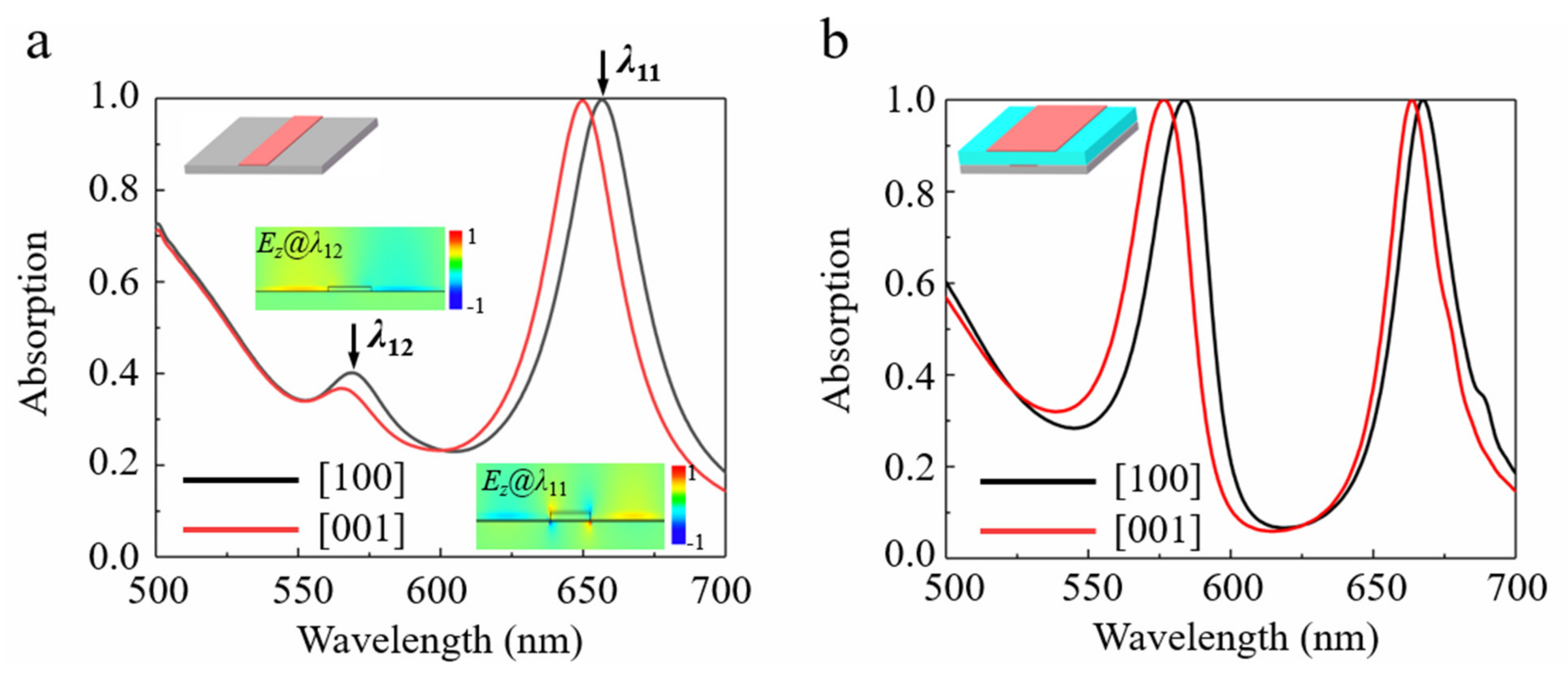
Figure 2a shows the simulated optical absorption spectra for the structure composed of a single layer α-MoO3 nanoribbon with a width w1 = 105 nm on a silver substrate when illuminated by polarized lights along [100] and [001] directions, respectively. It can be found from Figure 2a that two resonant peaks exist for both polarizations. When the incident light is polarized along the [100] direction, perfect absorption is achieved at λ11 = 657.4 nm. One can conclude from the z-components of electrical field in Figure 2a that the perfect absorption peak mainly originates from the resonant excitation of grating modes, which is caused by periodicity, as explained in reference [40]. By contrast, weak resonant absorption at the wavelength of λ12 = 569.2 nm is due to the excitation of the localized surface plasmons on the interface of metal Ag because of the existence of α-MoO3 nanoribbon grating. In addition, the resonant absorption peak has a blue-shift when polarization is switched to the [001] direction of α-MoO3. Interestingly, when a second α-MoO3 nanoribbon with a width w2 = 275 nm is stacked on the first α-MoO3 nanoribbon separated by a dielectric layer, as shown by the inset in Figure 2b, dual-band perfect absorption can be established for both polarization directions due to the absorption enhancement of the weak resonant absorption peak at the short wavelengths.

Figure 2.
(a) Simulated absorption spectra of the α-MoO3 nanoribbon stacked on Ag substrate, as polarized light along [100] (black curve) and [001] directions (red curve), respectively. (b) Simulated absorption spectra for the structure composed of Ag substrate/α-MoO3 nanoribbons/SiO2 dielectric layer/α-MoO3 nanoribbons from bottom to top, as polarized along [100] (black curve) and [001] (red curve) directions, respectively. The optimized geometrical parameters are listed as follows: w1 = 105 nm, w2 = 275 nm, h = 100 nm, p = 500 nm.
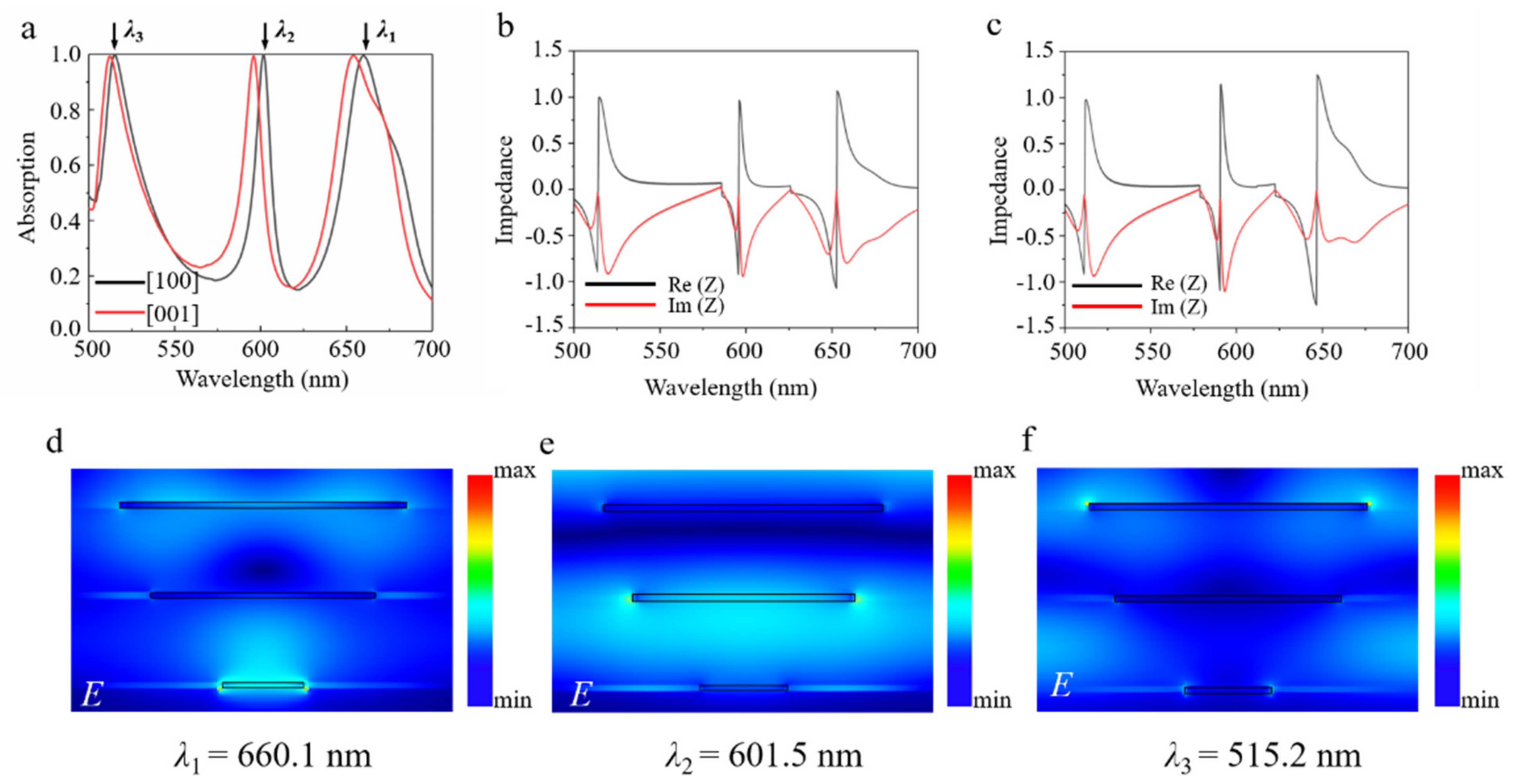
Based on the above analysis, one can expect that more perfect absorbing bands could be obtained with multiple stacking of α-MoO3 nanoribbon/dielectric layer. As displayed in Figure 3a, triple-band perfect absorption with recognizable anisotropy is observed by three stacking layers of α-MoO3 nanoribbon/dielectric on Ag substrate. Specifically, when the incident light is polarized along [100] direction of α-MoO3, three absorbing peaks locate at λ1 = 660.1 nm, λ2 = 601.5 nm, and λ3 = 515.2 nm, with corresponding absorptivity up to 99.5%, 99.7%, and 99.6%, separately. Moreover, the effective impedance of such an absorber is calculated according to Equation (2), as shown in Figure 3b. When the polarization is along [100] direction of α-MoO3, the corresponding effective impedances at the three resonant absorption peaks are Z1 = 0.996 − 0.152i, Z2 = 0.988 − 0.124i, and Z3 = 1.081 + 0.021i, separately. Obviously, all the effective impedances match quite well with the normalized impedance of free space, which indicates that optical reflection is suppressed effectively, thus resulting in the triple-band optical perfect absorption. In addition, three resonant absorption peaks also exist, and they remain in perfect absorbance while switching the polarization incidence along the [001] direction of α-MoO3. Meanwhile, all the resonant peaks shift to the shorter wavelengths due to the anisotropic lattice structure. The corresponding effective impedances at the three resonant absorption peaks are Z1 = 0.985 − 0.084i, Z2 = 1.127 − 0.124i, and Z3 = 1.251 + 0.013i, separately. Additionally, the real and imaginary parts of the effective impedances of those three peaks under such a circumstance match well with those of the free space, as shown in Figure 3c.
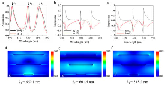
Figure 3.
(a) Simulated absorption spectra for the proposed triple layer α-MoO3 structure along [100] and [001] directions, respectively. (b,c) The calculated real and imaginary parts of the effective impedance along the [100] and [001] directions, respectively. The optimized geometrical parameters are listed as follows: h = 100 nm, w1 = 105 nm, w2 = 275 nm, w3 = 345 nm, p = 500 nm. (d–f) The calculated distribution of total electric field at the resonant wavelengths of λ1 = 660.1 nm, λ2 = 601.5 nm, and λ3 = 515.2 nm, separately.
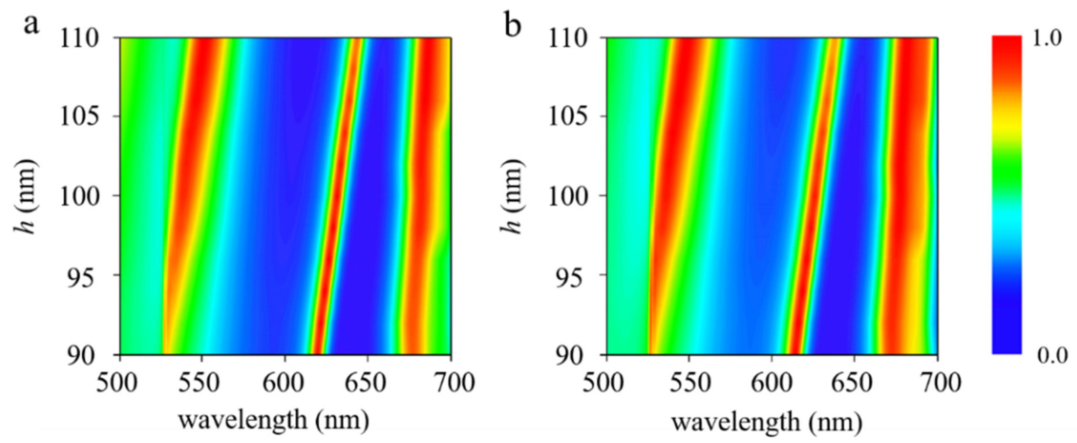
To interpret the underlying physics mechanism behind the multi-band perfect absorbing phenomenon, we calculate, in Figure 3d–f, the field distributions on the x–z plane at the different resonant frequencies, i.e., λ1 = 660.1 nm, λ2 = 601.5 nm, and λ3 = 515.2 nm, for polarization along the [100] direction of α-MoO3. From Figure 3d–f, one can see that the localized electric field is enhanced at the edges of α-MoO3 nanoribbons for each layer, which corresponds to the different resonant responses. In particular, at the wavelength of λ1 = 660.1 nm, the electric field hot spot is mainly excited in the bottom α-MoO3 nanoribbon, and the resonant wavelength is roughly consistent with λ11 = 657.4 nm in a one-layer α-MoO3 nanoribbon structure, which is referred to as grating mode. However, at the wavelengths of λ2 = 601.5 nm and λ3 = 515.2 nm, electric energies are strongly concentrated on the edges of middle and top α-MoO3 nanoribbons, respectively. For the both cases, the stacking α-MoO3/dielectric layers on a silver mirror form the Fabry–Pérot cavity, and the resonant absorption mainly results from the cavity modes’ interference effect. The incident light is reflected back and forth between the α-MoO3 nanoribbons and metal substrate, with a complex propagation phase , where is the permittivity of the spacer, k0 is the wavenumber in free space, and h is the dielectric thickness. The absorbance can be derived from , where is the total reflection resulting from the superposition of multiple reflections. Obviously, spacer thickness h plays a major role. Figure 4a,b depicts the absorption spectra of the proposed structure as a function of wavelength and the thickness of SiO2 dielectric layer. It is clearly seen from Figure 4 that the dielectric thickness directly affects the resonance wavelength of the Fabry–Pérot cavity. With the increase in SiO2 layer thickness, all three resonance peaks shift to a long wavelength. The maximum absorbance occurs at the constructive interference, with a phase condition of , where ϕ represents the reflection phase shift and m is an integer.
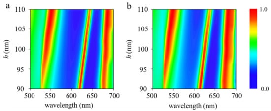
Figure 4.
Absorption spectra of the proposed structure as a function of wavelength and the height of SiO2 dielectric layer h, with polarization along (a) [100] and (b) [001] crystalline directions of α-MoO3.
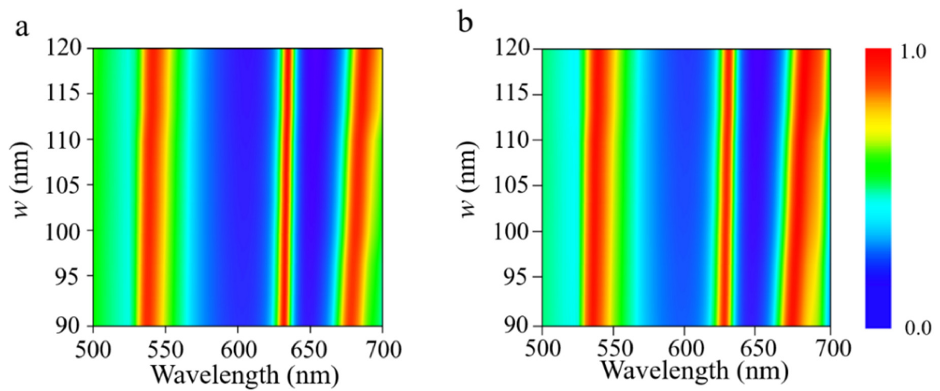
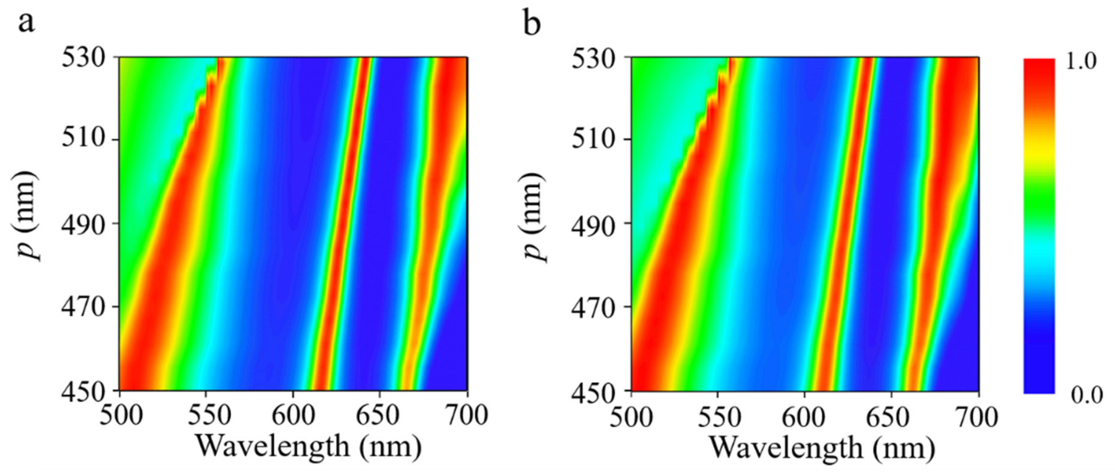
Figure 5 illustrates the optical absorption as a function of incident wavelength and widths of the three α-MoO3 nanoribbons. The width ratio constant with w3/w2 = 1.3, w2/w1 = 2.6, respectively. While increasing the width of the nanoribbons, the distance of the nanoribbons in the adjacent period shortens and the interaction increases; all the resonant absorbing peaks exhibit a minor shifting to the longer wavelengths, and absorptivity is higher than 90%. The reason can be attributed to the fact that the wider α-MoO3 nanoribbons support the electromagnetic responses at longer wavelengths. Besides, Figure 6 shows the influence of periodicity on the absorption spectra for both [100] and [001] polarizations. Apparently, all the resonant peaks shift toward the longer wavelength while increasing the periodicity of the α-MoO3 absorber. As the period becomes larger, the distance between adjacent α-MoO3 nanoribbons enlarges as well. As a result, the interaction between them creates a change, thus leading to a shifting of resonant frequencies. In short, it can be concluded that a multi-band α-MoO3-based perfect absorber in visible frequencies can be optimized by changing the geometrical parameters of the structure.
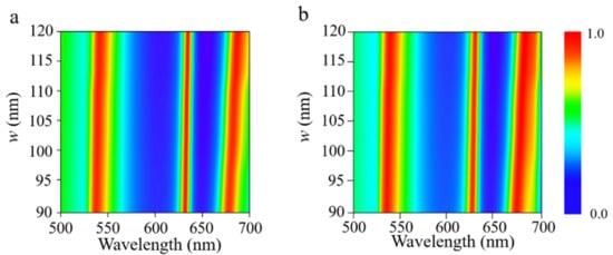
Figure 5.
Absorption spectra of the proposed structure as a function of wavelength and the width w of α-MoO3 nanoribbons with polarization along (a) [100] and (b) [001] crystalline directions of α-MoO3; the width ratio constant is kept unchanged.
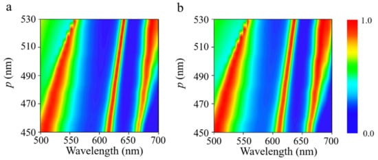
Figure 6.
Absorption contour of the proposed structure as a function of wavelength and periodicity p of the proposed structure for incident polarization along (a) [100] and (b) [001] crystalline directions of α-MoO3.
4. Conclusions
In conclusion, we theoretically propose and numerically demonstrate an anisotropic perfect metamaterial absorber in visible frequencies; it consists of a multi-layered α-MoO3/dielectric structure stacked on a silver mirror. Additionally, the number of perfect absorption bands is closely related to the α-MoO3 nanoribbon/dielectric layers. When the proposed absorber is composed of three α-MoO3 nanoribbon/dielectric layers, the electromagnetic simulations show that triple-band perfect absorption can be achieved for polarization along the [100] and [001] directions of α-MoO3, respectively. Additionally, the calculation results obtained by FDTD method are consistent with the effective impedance of the designed absorber. The physical mechanism of the perfect absorption can be attributed to the resonant grating modes and the interference effect of Fabry–Pérot cavity modes. In addition, we have calculated and analyzed the absorption spectra of the proposed structure as a function of wavelength and the related geometrical parameters in detail. Moreover, our method can be flexibly extended to obtain a tunable multi-band perfect absorber in the visible frequencies by adjusting the numbers of layers in the α-MoO3/dielectric stacking structure. Our research opens up an avenue for designing anisotropic meta-devices with tunable spectra, and it has potential applications in spectral imaging, photodetectors, and sensors.
Author Contributions
Conceptualization, B.T. and N.Y.; methodology, N.Y.; software, N.Y.; validation, B.T., N.Y., X.S., G.J. and J.S.; formal analysis, B.T.; investigation, N.Y.; resources, X.S.; data curation, G.J.; writing—original draft preparation, N.Y.; writing—review and editing, B.T.; visualization, G.J. and J.S.; supervision, B.T.; project administration, B.T.; funding acquisition, B.T. and G.J. All authors have read and agreed to the published version of the manuscript.
Funding
This research was funded by Natural Science Foundation of Jiangsu Province (BK20201446) and the Innovation and Entrepreneurship Training Program for College Students (2020-191-3670).
Conflicts of Interest
The authors declare no conflict of interest.
References
- Zhang, Y.; Feng, Y.; Zhao, J. Graphene-enabled tunable multifunctional metamaterial for dynamical polarization manipulation of broadband terahertz wave. Carbon 2020, 163, 244–252. [Google Scholar] [CrossRef]
- Song, L.; Ci, L.; Lu, H.; Sorokin, P.B.; Jin, C.; Ni, J.; Kvashnin, A.G.; Kvashnin, D.G.; Lou, J.; Yakobson, B.I.; et al. Large scale growth and characterization of atomic hexagonal boron nitride layers. Nano Lett. 2010, 10, 3209–3215. [Google Scholar] [CrossRef] [PubMed]
- Deng, G.; Song, X.; Dereshgi, S.A.; Xu, H.; Aydin, K. Tunable multi-wavelength absorption in mid-IR region based on a hybrid patterned graphene-hBN structure. Opt. Express 2019, 27, 23576–23584. [Google Scholar] [CrossRef]
- Min, B.K.; Nguyen, V.-T.; Kim, S.J.; Yi, Y.; Choi, C.-G. Surface Plasmon Resonance-Enhanced Near-Infrared Absorption in Single-Layer MoS2 with Vertically Aligned Nanoflakes. ACS Appl. Mater. Interfaces 2020, 12, 14476–14483. [Google Scholar] [CrossRef] [PubMed]
- Liu, Z.; Aydin, K. Localized Surface Plasmons in Nanostructured Monolayer Black Phosphorus. Nano Lett. 2016, 16, 3457–3462. [Google Scholar] [CrossRef] [PubMed]
- Tang, B.; Yang, N.; Huang, L.; Su, J.; Jiang, C. Tunable Anisotropic Perfect Enhancement Absorption in Black Phosphorus-Based Metasurfaces. IEEE Photon. J. 2020, 12, 1–9. [Google Scholar] [CrossRef]
- Xiong, F.; Zhang, J.; Zhu, Z.; Yuan, X.; Qin, S. Strong anisotropic perfect absorption in monolayer black phosphorous and its application as tunable polarizer. J. Opt. 2017, 19, 075002. [Google Scholar] [CrossRef]
- Jia, Z.; Huang, L.; Su, J.; Tang, B. Tunable plasmon-induced transparency based on monolayer black phosphorus by bright-dark mode coupling. Appl. Phys. Express 2020, 13, 072006. [Google Scholar] [CrossRef]
- Ajayan, P.; Kim, P.; Banerjee, K. Two-dimensional van der Waals materials. Phys. Today 2016, 69, 38–44. [Google Scholar] [CrossRef] [Green Version]
- Ma, W.; Alonso-Gonzalez, P.; Li, S.; Nikitin, A.Y.; Yuan, J.; Martin-Sanchez, J.; Taboada-Gutierrez, J.; Amenabar, I.; Li, P.; Velez, S.; et al. In-plane anisotropic and ultra-low-loss polaritons in a natural van der Waals crystal. Nature 2018, 562, 557–562. [Google Scholar] [CrossRef] [Green Version]
- Taboada-Gutierrez, J.; Alvarez-Perez, G.; Duan, J.; Ma, W.; Crowley, K.; Prieto, I.; Bylinkin, A.; Autore, M.; Volkova, H.; Kimura, K.; et al. Broad spectral tuning of ultra-low-loss polaritons in a van der Waals crystal by intercalation. Nat. Mater. 2020, 19, 964–968. [Google Scholar] [CrossRef]
- Lajaunie, L.; Boucher, F.; Dessapt, R.; Moreau, P. Strong anisotropic influence of local-field effects on the dielectric response of α-MoO3. Phys. Rev. B 2013, 88, 115141. [Google Scholar] [CrossRef] [Green Version]
- Wei, C.; Abedini Dereshgi, S.; Song, X.; Murthy, A.; Dravid, V.P.; Cao, T.; Aydin, K. Polarization Reflector/Color Filter at Visible Frequencies via Anisotropic α-MoO3. Adv. Opt. Mater. 2020, 8, 2000088. [Google Scholar] [CrossRef]
- Hu, G.; Ou, Q.; Si, G.; Wu, Y.; Wu, J.; Dai, Z.; Krasnok, A.; Mazor, Y.; Zhang, Q.; Bao, Q. Observation of topological polaritons and photonic magic angles in twisted van der Waals bi-layers. Nature 2020, 582, 209–213. [Google Scholar] [CrossRef]
- Abedini Dereshgi, S.; Folland, T.G.; Murthy, A.A.; Song, X.; Tanriover, I.; Dravid, V.P.; Caldwell, J.D.; Aydin, K. Lithography-free IR polarization converters via orthogonal in-plane phonons in alpha-MoO3 flakes. Nat. Commun. 2020, 11, 5771–5779. [Google Scholar] [CrossRef] [PubMed]
- Tang, B.; Zhu, Y.; Zhou, X.; Huang, L.; Lang, X. Wide-Angle Polarization-Independent Broadband Absorbers Based on Concentric Multisplit Ring Arrays. IEEE Photon. J. 2017, 9, 1–7. [Google Scholar] [CrossRef]
- Wu, J.; Jiang, L.; Guo, J.; Dai, X.; Xiang, Y.; Wen, S. Turnable perfect absorption at infrared frequencies by a Graphene-hBN Hyper Crystal. Opt. Express 2016, 24, 17103–17114. [Google Scholar] [CrossRef] [PubMed]
- Wang, T.; Qu, L.; Qu, L.; Zhang, Y.; Zhang, H.; Cao, M. Tunable broadband terahertz metamaterial absorber using multi-layer black phosphorus and vanadium dioxide. J. Phys. D 2020, 53, 145105. [Google Scholar] [CrossRef]
- Huang, X.; He, W.; Yang, F.; Ran, J.; Gao, B.; Zhang, W.-L. Polarization-independent and angle-insensitive broadband absorber with a target-patterned graphene layer in the terahertz regime. Opt. Express 2018, 26, 25558–25566. [Google Scholar] [CrossRef] [PubMed]
- Deng, G.; Yang, J.; Yin, Z. Broadband terahertz metamaterial absorber based on tantalum nitride. Appl. Opt. 2017, 56, 2449–2454. [Google Scholar] [CrossRef] [PubMed]
- Landy, N.I.; Sajuyigbe, S.; Mock, J.J.; Smith, D.R.; Padilla, W.J. Perfect metamaterial absorber. Phys. Rev. Lett. 2008, 100, 207402. [Google Scholar] [CrossRef]
- Chen, F.; Cheng, Y.; Luo, H. Temperature Tunable Narrow-Band Terahertz Metasurface Absorber Based on InSb Micro-Cylinder Arrays for Enhanced Sensing Application. IEEE Access 2020, 8, 82981–82988. [Google Scholar] [CrossRef]
- Khonina, S.N.; Butt, M.A.; Kazanskiy, N.L. Numerical investigation of metasurface narrowband perfect absorber and a plasmonic sensor for a near-infrared wavelength range. J. Opt. 2021, 23, 065102. [Google Scholar] [CrossRef]
- Aydin, K.; Ferry, V.E.; Briggs, R.M.; Atwater, H.A. Broadband polarization-independent resonant light absorption using ultrathin plasmonic super absorbers. Nat. Commun. 2011, 2, 1–7. [Google Scholar] [CrossRef]
- Sang, T.; Qi, H.; Wang, X.; Yin, X.; Li, G.; Niu, X.; Ma, B.; Jiao, H. Ultrabroadband Absorption Enhancement via Hybridization of Localized and Propagating Surface Plasmons. Nanomaterials 2020, 10, 1625. [Google Scholar] [CrossRef]
- Tang, B.; Li, Z.; Palacios, E.; Liu, Z.; Butun, S.; Aydin, K. Chiral-selective plasmonic metasurface absorbers operating at visible frequencies. IEEE Photon. Technol. Lett. 2017, 29, 295–298. [Google Scholar] [CrossRef]
- Yi, Z.; Li, J.; Lin, J.; Qin, F.; Chen, X.; Yao, W.; Liu, Z.; Cheng, S.; Wu, P.; Li, H. Broadband polarization-insensitive and wide-angle solar energy absorber based on tungsten ring-disc array. Nanoscale 2020, 12, 23077–23083. [Google Scholar] [CrossRef]
- Huang, S.; Xie, Z.; Chen, W.; Lei, J.; Wang, F.; Liu, K.; Li, L. Metasurface with multi-sized structure for multi-band coherent perfect absorption. Opt. Express 2018, 26, 7066–7078. [Google Scholar] [CrossRef]
- Wang, X.; Wang, Q.; Dong, G.; Hao, Y.; Lei, M.; Bi, K. Multi-band terahertz metasurface absorber. Mod. Phys. Lett. B 2017, 31, 1750354. [Google Scholar] [CrossRef]
- Kokilavani, S.; Syed, A.; Thomas, A.M.; Elgorban, A.M.; Al-Rashed, S.; Raju, L.L.; Khan, S.S. Integrating Ag2WO4 on VS4 nanoplates with synergy of plasmonic photocatalysis and boosted visible-light harvesting and its antibacterial applications. J. Alloy. Compd. 2021, 865, 158810. [Google Scholar] [CrossRef]
- Jiang, K.; Sun, X.; Zhang, Z.-H.; Ben, J.; Che, J.; Shi, Z.; Jia, Y.; Chen, Y.; Zhang, S.; Lv, W.; et al. Polarization-enhanced AlGaN solar-blind ultraviolet detectors. Photonics Res. 2020, 8, 1243–1252. [Google Scholar] [CrossRef]
- Kanté, B.; de Lustrac, A.; Lourtioz, J.-M.; Burokur, S.N. Infrared cloaking based on the electric response of split ring resonators. Opt. Express 2008, 16, 9191–9198. [Google Scholar] [CrossRef] [PubMed]
- Luo, X.; Liu, Z.; Wang, L.; Liu, J.; Lin, Q. Tunable ultra-narrowband and wide-angle graphene-based perfect absorber in the optical communication region. Appl. Phys. Express 2018, 11, 105102. [Google Scholar] [CrossRef]
- Zhu, Y.; Tang, B.; Jiang, C. Tunable ultra-broadband anisotropic absorbers based on multi-layer black phosphorus ribbons. Appl. Phys. Express 2019, 12, 032009. [Google Scholar] [CrossRef]
- Zhu, Y.; Tang, B.; Yang, N.; Lang, X.; Su, J.; Li, Z. Tunable wide-angle perfect absorber based on black phosphorous-dielectric-metallic hybrid architecture. Phys. E Low Dimens. Syst. Nanostruct. 2021, 126, 114449. [Google Scholar] [CrossRef]
- Qi, H.; Sang, T.; Yin, X.; Wang, X.; Li, G. Dual-band absorption enhancement of monolayer molybdenum disulfide by a tapered metamaterial waveguide slab. Appl. Phys. Express 2020, 13, 065001. [Google Scholar] [CrossRef]
- Deng, G.; Dereshgi, S.A.; Song, X.; Wei, C.; Aydin, K. Phonon-polariton assisted broadband resonant absorption in anisotropic α-phase MoO3 nanostructures. Phys. Rev. B 2020, 102, 035408. [Google Scholar] [CrossRef]
- Dong, D.; Liu, Y.; Fu, Y. Critical Coupling and Perfect Absorption Using α-MoO3 Multilayers in the Mid-Infrared. Ann. Der Phys. 2021, 533, 2000512. [Google Scholar] [CrossRef]
- Smith, D.R.; Vier, D.C.; Koschny, T.; Soukoulis, C.M. Electromagnetic parameter retrieval from inhomogeneous metamaterials. Phys. Rev. E Stat. Nonlin. Soft. Matter. Phys. 2005, 71, 036617. [Google Scholar] [CrossRef] [Green Version]
- Byelobrov, V.O.; Zinenko, T.L.; Kobayashi, K.; Nosich, A.I. Periodicity Matters: Grating or lattice resonances in the scattering by sparse arrays of subwavelength strips and wires. IEEE Antennas Propag. Mag. 2015, 57, 34–45. [Google Scholar] [CrossRef]
Publisher’s Note: MDPI stays neutral with regard to jurisdictional claims in published maps and institutional affiliations. |
© 2021 by the authors. Licensee MDPI, Basel, Switzerland. This article is an open access article distributed under the terms and conditions of the Creative Commons Attribution (CC BY) license (https://creativecommons.org/licenses/by/4.0/).

