Article

Optimized Planar Microwave Antenna for Nitrogen Vacancy Center Based Sensing Applications

Department of Physics, University of Kaiserslautern, Erwin-Schrödinger-Straße, 67663 Kaiserslautern, Germany
*
Author to whom correspondence should be addressed.
Nanomaterials 2021, 11(8), 2108; https://doi.org/10.3390/nano11082108
Submission received: 23 June 2021 / Revised: 12 August 2021 / Accepted: 12 August 2021 / Published: 19 August 2021
(This article belongs to the Special Issue Nano Devices and Nano Sensors)

Abstract

:
Individual nitrogen vacancy (NV) color centers in diamond are versatile, spin-based quantum sensors. Coherently controlling the spin of NV centers using microwaves in a typical frequency range between 2.5 and 3.5 GHz is necessary for sensing applications. In this work, we present a stripline-based, planar, Ω -shaped microwave antenna that enables one to reliably manipulate NV spins. We found an optimal antenna design using finite integral simulations. We fabricated our antennas on low-cost, transparent glass substrate. We created highly uniform microwave fields in areas of roughly 400 × 400 μm2 while realizing high Rabi frequencies of up to 10 MHz in an ensemble of NV centers.

1. Introduction

Nitrogen vacancy (NV) centers in diamond each consist of a substitutional nitrogen atom and an adjacent lattice vacancy. In recent years, this crystal defect in its negatively charged form, NV , has been extensively studied as a versatile spin-based quantum sensor (for simplicity, we use the term NV center for the negatively charged state throughout this manuscript). The NV center forms an electronic S = 1 spin system with a zero field splitting (ZFS) of 2.87 GHz between the m s = 0 and the degenerate m s = ±1 ground state. Manipulating these highly-coherent spin states is accomplished using microwaves (MW), e.g., via coherent oscillations (Rabi oscillations). These form the basis of spin-based quantum sensing using NV centers. An external magnetic field parallel to the NV’s high symmetry axis lifts the degeneracy between m s = ±1 states via the Zeeman effect, whereas a perpendicular field induces spin mixing. In addition, mechanical pressure, temperature and electrical fields interact with the NV spin, consequently making it a versatile atomic scale sensor [1,2,3,4,5,6,7,8]. To fully harness the NV’s sensing capabilities, providing spatially homogeneous, intense MW fields which are stable over long periods of measurement within well-defined volumes remains an on-going challenge. In this work, we investigate planar, micro-fabricated MW antennas to reliably deliver MW radiation to NV sensors.
NV centers are among the most promising candidates for many quantum technological applications due to their feasible spin initialization, read-out and manipulation using laser light (mostly around 532 nm) and MW fields [9]. An intersystem crossing in the NV center’s energy level scheme allows for spin state initialization by optical pumping and optical readout via spin dependent fluorescence [10,11]. The effect is known as optically detected magnetic resonance (ODMR, for details refer to [12,13]). ODMR using continuous MW is the most basic sensing mode using NVs (DC magnetometry). AC magnetometry employs pulsed MW sequences, e.g., spin-echo [14], or more advanced dynamical decoupling protocols [15,16,17,18,19,20].
Sensing with NVs can be typically divided into two approaches, either exploiting the atomic scale size of a single NV center to enable high resolution magnetometry, or sacrificing the latter in favor of highly sensitive magnetometry with an enhanced signal to noise ratio and enhanced sensitivity using an ensemble of NV centers. Sensing using ensembles requires highly homogeneous MW fields, as any field inhomogeneity over the ensemble constitutes a dephasing and consequently reduces sensitivity [21,22,23,24,25,26,27,28,29,30,31,32,33]. Additionally, for single NV-based schemes, spatially homogeneous fields are relevant, especially when scanning NV centers are used to image samples [13,34,35,36,37,38,39,40,41].
For AC magnetometry, the sensitivity depends on the coherence time T 2 , which can be enhanced by employing dynamical decoupling protocols. In such multipulse protocols, short, intense MW pulses are of interest to perform full pulse sequences within the potentially low coherence and dephasing times of NV centers. This demand for homogeneous, stable and intense MW fields motivated our work for an optimized MW antenna design for NV sensing.
In this study, we investigate MW antenna designs compatible with confocal and atomic force microscopy (AFM) based sensing applications with NV centers (Figure 1a) [13,34,35,36,37,38,39,40,41]. Commonly used antenna concepts have design-related limitations with respect to these applications: Wire antennas suffer from inhomogeneity in the radiated fields requiring precise positioning [42]. Stripline antennas tend to be large in size and overload piezo scanners in confocal microscopes when placed on top [43,44,45,46]. Coil antennas only radiate MW of low amplitude [47,48,49]. Resonators are limited in bandwidth [50,51,52,53,54,55,56].
We aimed for planar antenna designs that can be efficiently incorporated into sensing setups without significant hardware modifications (Figure 1a). To investigate larger microstructures, e.g., biological samples with characteristic dimensions of the order of several hundred μ m, one aims for macroscopically large and homogeneously radiated MW fields of high amplitude. The stripline-based design we made offers risk-free sample handling by mounting the sample on top of the antenna, implementation without blocking optical access and the advantage of established fabrication technology. By using transparent substrates for the antenna, we provide an antenna design that also allows observation in inverted geometries where the optical path crosses the antenna or the antenna is attached to the microscope objective [25,57]. We made a design based on an Ω -shape (Figure 1b). This layout inherently leads to the radiation of a homogeneous MW field within the aperture towards the designated sample volume (see inset Figure 1b).
Our manuscript is structured as follows: Section 2 summarizes the process flow, relevant materials and parameters for our MW antenna fabrication. Section 3 summarizes the methodology, assumptions and numerical simulation approach to find an optimized antenna design. Section 4 briefly describes the experimental setup and methods to characterize and test the antennas. Section 5 discusses our experimental findings on the MW antenna performance.

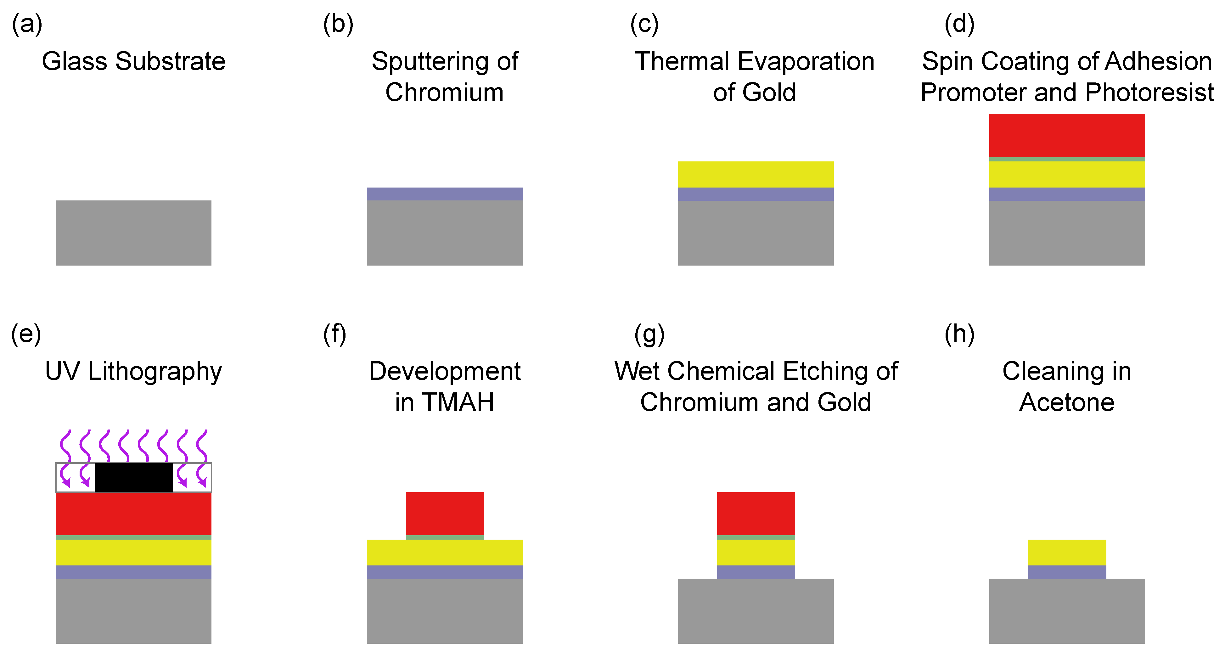
2. Microfabrication Methods

We fabricated the antennas on borosilicate glass substrates (relative permittivity ϵ r = 4.82, substrate thickness s z = 1 mm; Figure 2a). To prepare thin film deposition, we cleaned the substrate in acetone followed by isopropanol using an ultrasonic bath. We removed absorbed water by heating the substrates on a heatplate (120 C, 10 min). We then used either sputtering or thermal evaporation to deposit an adhesion layer (20 nm chromium) (Figure 2b) followed by a 100 nm gold layer (Figure 2c). To fabricate the antenna structure, we used spin coating (6000 rpm, 1 min) followed by baking (120 C, 2 min) to deposit an adhesion promoting sub-monolayer of TI Prime (MicroChemicals, Ulm, Germany). We then spin coated the photoresist AZ1518 (6000 rpm, 1 min, Merck, Darmstadt, Germany) (Figure 2d). After a prebake (100 C, 50 s), we applied contact UV lithography using a laser written binary intensity amplitude chromium photomask (Figure 2e). Lithography parameters were chosen according to resist manufacturer specifications resulting in an area dose of 33.6 mJ cm 2 . We developed the resist mask by stirring the exposed substrates in TMAH (Acros Organics, Fair Lawn, NJ, USA) 2.5% in water (Figure 2f). After rinsing it in monodistilled water, we performed a postbake (120 C, 50 s). To form the antenna structure using wet chemical etching: First, we stirred the substrate in gold etchant (Sigma-Aldrich, St. Louis, MI, USA) followed by rinsing it in chromium etchant (Sigma-Aldrich, Figure 2g). To remove residual photoresist and potential contamination, we stirred the fabricated MW antenna in acetone and isopropanol (Figure 2h). This allowed electrical contacting by gluing SMT ultra-miniature coaxial connectors (U.FL-R-SMT(01), Hirose Electronic, Tokyo, Japan) using electrically conductive epoxy adhesives (EPO-TEK H20E, Epoxy Technology, Billerica, MA, USA).

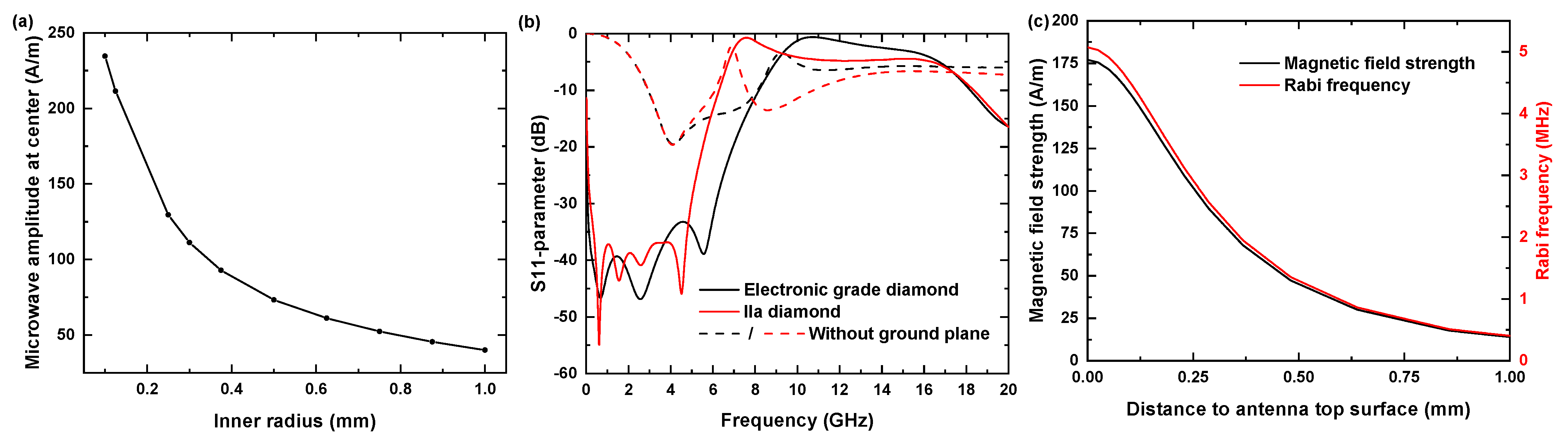
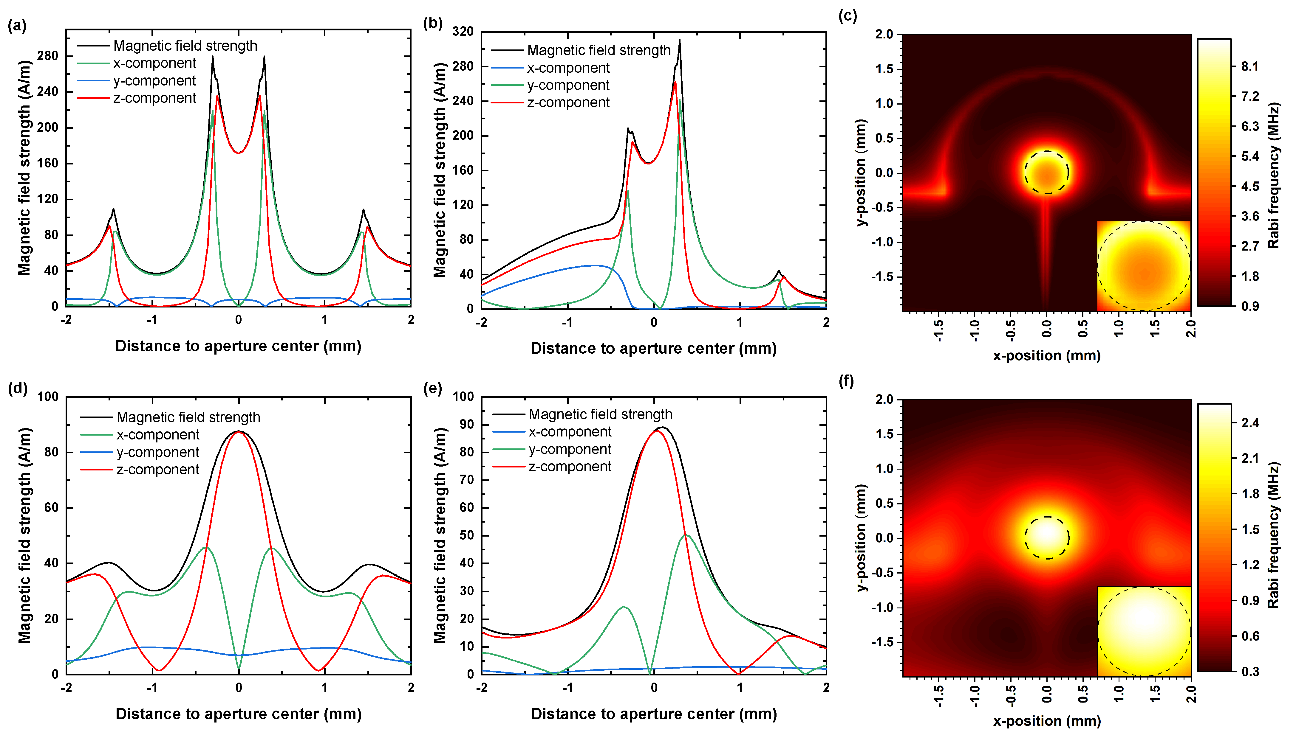
3. Numerical Simulation and Optimization

For the numerical optimization, we used the time domain solver of the commercial software CST Microwave Studio (Dassault Systèmes, Vélizy-Villacoublay, France), which uses the finite integral technique (FIT) to solve the Maxwell equations [58]. We defined waveguide ports at the ends of the microstripline, where waveguide modes could leave or enter the domain of interest. During each simulation, the total MW power delivered at the excited port was 500 mW. We typically ran the simulation in the frequency range between 2 and 4 GHz. To enhance far field calculation accuracy, our simulation included additional space between the structure and the simulated space boundaries ( λ MW 4 26 mm). The boundaries fulfilled the perfectly matched layer (PML) condition, assuring that incident waves were being absorbed with negligible back reflections. The applied mesh exhibited variable mesh cell sizes and was locally refined by introducing additional cells within the space around critical structural features, such as corners, edges and material interfaces. This approach allows for highly precise simulations while keeping computational time reasonable. Due to the varying structure geometries, the simulated space was typically meshed with approximately 180 × 190 × 140 cells, resulting in 4.6 million cells involving a total volume of roughly 68 mm × 63 mm × 54 mm.
The linear and radial parts of the antenna form capacitive and inductive components, respectively. Altogether, they determine the antenna’s resonance. To harness this antenna design for NV-based sensing, we optimized the linear and radial geometry to match antenna resonance and NV spin transition frequency. Consequently, the main parameters to be optimized were the gap width g w and the radial width r w of the Ω -antenna (see Figure 1b). In addition, optimizing the feedline width f w also yielded a slight improvement. We also considered the thickness of the gold layer t Au forming the conductor. Our results indicate a negligible influence on resonance frequency and field distribution for films thinner than 1 μ m. Furthermore, we did not observe significant improvement capabilities by increasing the layer thickness further. All simulated gold layers are thinner than the theoretically expected skin depth for gold of 1.4 μ m at 2.87 GHz, leading to an approximately homogeneous current density throughout the gold layer. We assume the contribution of the chromium adhesion layer to the antenna properties to be negligible. We thus did not vary the thickness of this layer and set it to 20 nm.
To achieve a high MW field within the aperture, the inner radius of the aperture should be minimized, contradicting the aim for a macroscopically large radiated area. For all optimization steps, we evaluated the magnetic field amplitude at the center of the antenna’s aperture at a distance of 10 nm below the diamond sample’s top surface, which corresponds to the approximate depth of shallow NV centers. For the diamond sample, we considered a (100)-oriented diamond (2.5 mm × 1.5 mm × 50 μ m). Typically, for experiments using single NV centers, high purity electronic grade, chemical vapor deposited diamonds (substitutional nitrogen content <5 ppb, manufacturer: Element Six, Didcot, United Kingdom) were used. For testing the antenna, we used less pure diamonds (substitutional nitrogen content <1 ppm, termed IIa diamonds) which were 300 μ m thick and contained dense ensembles of NV centers, which we also considered for better comparison with our experimental results. Note that for the simulations, the dielectric constant used for electronic grade and IIa diamonds was identical, as it was not influenced by the nitrogen content. By varying the inner radius of the aperture, we found a trade-off between the achievable MW amplitude and the radiated area size, as shown in Figure 3a. We chose the inner radius to be 300 μ m, which was smaller than the diamond under consideration, but allows one to investigate reasonably large sample areas. Note that only for an inner radius value of 300 μ m, the design was fully optimized. For all other values, we expected the amplitude could be further enhanced subjecting to the repeated optimization of the remaining parameters. Otherwise, these calculations assumed the same parameter values we determined during the optimization for an inner radius of 300 μ m.
We set the lateral substrate size to 16 mm × 11 mm. This substrate allowed for straightforward mounting to typical piezo-scanner in confocal microscope setups. The simulation also included the sample holder which we assumed to be a 24 mm × 15 mm titanium plate, as compliant with the piezo scanner systems (attocube systems, Haar, Germany) used in our setup.
For the optimization, we applied the software’s internal goal function by defining quantities and frequency ranges in which they were evaluated, type of goal (minimization/maximization) and weight factors. We consider different aspects relevant for the antenna performance. The predominant limitation in maximizing the radiated field amplitude was given by a frequency mismatch leading to significant back reflections of the input MW signal characterized by the high frequency circuitry component’s S 11 -parameter. In accordance with other reported work, we minimized the S 11 -parameter of the antenna and consequently the back reflection of the input signal at 2.87 GHz [45,46,47,51,52,53,54,56]. Optimizing the Ω -antenna for NV sensing involving variable, high magnetic bias fields, and for obtaining complete ODMR spectra, required us to maximize the antenna bandwidth. To account for that, we extended the minimization of S 11 to the frequency range between 2.77 and 2.97 GHz. Overall, we performed two evaluations of S 11 , once individually at 2.87 GHz, and again in the range between 2.77 and 2.97 GHz. Both the evaluations were given equal weight, allowing us to maximize the bandwidth and simultaneously favor a centering of the resonance at 2.87 GHz. Furthermore, our optimization goal function aimed to maximize the magnetic field strength. The weight factor was chosen accordingly to allow for equal contributions between the S 11 -parameter and the target microwave amplitude.
Under these assumptions, we determined the following set of optimized geometry parameters: gap width g w = 7 μ m, radial width r w = 1.151 mm, feedline width f w = 1.851 mm. This antenna structure exhibits multiple resonances at 0.7, 2.6 and 5.5 GHz. For the most relevant resonance at 2.5 GHz, we found a value of −47 dB, as illustrated by the S 11 -parameter curve in Figure 3b. For the optimized case of 50 μ m thick electronic grade diamonds, the bandwidth for this structure amounts to 8.2 GHz, enabling reliable NV spin manipulation involving bias fields up to 190 mT. For 300 μ m thick IIa diamonds, our results indicate a lowering of the bandwidth down to 6.3 GHz, consequently limiting feasible bias fields to 120 mT. Our titanium sample holder acted as a ground plane and significantly decreased back reflections. To estimate the Ω -antenna’s robustness against geometry deviations arising from UV lithography tolerance errors, we repeated the simulation and adjusted either the gap width by ±1 μ m or the radial width by ±10 μ m and compared the respective S 11 -parameter curves. We found slight resonance shifts of approximately −50 MHz/ μ m for increasing gap width and −20 MHz/ μ m for increasing radial width. Together with its wideband resonance property, this design is suited for versatile applications in the field of NV-based sensing [21,23,25,26,27,28,29,30,31,32,33,34,35,36,38,39,40,41].
With increasing distance to the antenna’s top surface we found a decrease in MW field amplitude (see Figure 3c). For NV-Centers very close to antenna’s top surface, the achievable Rabi frequencies at the aperture center reached values of up to 5.1 MHz. For coherent spin manipulation of shallow NV centers, we found in 50 μ m electronic grade diamonds and 300 μ m thick IIa diamonds Rabi frequencies of 4.9 and 2.5 MHz. Due to an approximate radial symmetry of the Ω -antenna, the established MW field distribution shows a radial distance dependence from the aperture center in the x-y plane (see Figure 4a,b). For an electronic grade diamond with 50 μ m thickness, the typically achieved value of the magnetic field amplitude exceeded 170 A m . Towards the aperture circumference, we observed a parabolic increase up to 280 A m . Within an area with a radius of 260 μ m, the total MW field is mainly given by its perpendicular z-component, as shown in Figure 4a,b. Beyond the circumference, there is a further increase in the amplitude due to a strong increase in the lateral field components, in contrast the z-component drops off quickly. In the direction of the gap, the MW field amplitudes do not reach the mentioned peak values and decrease near it instead. From the field distribution, we calculated the expected Rabi frequency Ω R considering detuning due to field components parallel to the NV axis for one subset of NV centers (see Figure 4c). For a square area fitting into the aperture (edge length 420 μ m), we determined an average value for the expected Ω R of 5.9 MHz ± 0.5 MHz. For later comparison with our experimental data, Figure 4d–f shows the simulation data for a IIa diamond of 300 μ m thickness. In that case we determined an average value for the expected Ω R of 2.38 ± 0.06 MHz.

4. Experimental Setup and Methods

To asses the performances of the microfabricated antennas, we applied them to typical methods used in NV-based sensing (see [12,13]). We mounted the antenna on a sample holder using a thin layer of Crystal Bond 509 (Structure Probe Inc, West Chester, PN, USA). As a sample, we used a single crystalline, (100)-oriented IIa, chemical vapor deposited diamond (Element Six, 3 mm × 3 mm × 300 μ m, substitutional nitrogen content <1 ppm). We cleaned the diamond in a tri-acid mixture (H 2 SO 4 96%, HClO 4 70%, HNO 3 65%) at 500 C for 1 h. The sample contained a homogeneous ensemble of native NV centers, as confirmed by multiple photoluminescence confocal scans.
We used a laboratory-built confocal microscope setup (numerical aperture NA = 0.8, excitation wavelength λ L a s e r = 532 nm). Confocal filtering of the NV ensemble’s fluorescence was realized by using a single mode optical fiber. To measure the fluorescence, we used a single photon detector (SPCM-AQRH-14, quantum efficiency ≈ 68%, Excelitas Technologies, Waltham, MA, USA) and a data acquisition card for acquiring and logging the signal (PCIe-6323, National Instruments, Austin, TX, USA).
We connected the Ω -antennas to an MW source (SG 384, Stanford Research Systems, Sunnyvale, CA, USA) with an amplifier (ZASWA-2-50DR+, typ. +30 dB, Mini Circuits, Brooklyn, NY, USA). We applied a static bias field by positioning a neodymium (NdFeB) permanent magnet using a three-axis linear stage. We aligned the bias field with one of the 111 crystal directions within an error of 15 .
We realized Rabi oscillations (see [59]), where we determined the achievable Rabi frequency Ω R in the NV spin system with the MW power deployed by the antenna. The Ω R is the prime measure for antenna performance because it depends linearly on the perpendicular component of the MW’s amplitude relative to the NV axis. These measurements were done for different positions to map the spatial homogeneity of the Rabi frequency. We also acquired continuous wave and pulsed optically detected magnetic resonance (ODMR) measurements (see [60]) and ran dynamical decoupling protocols (see [61]) showing the suitability of the MW antenna design for nanoscale NV-based sensing applications.
To generate the control MW pulses used in dynamical decoupling experiments, we used the in-built digital I/Q mixer of the MW signal generator in combination with external quadrature signal sources (Pulse Streamer 8/2, Swabian Instruments, Stuttgart, Germany). With this approach, we controlled the pulse duration, shape and polarity of the MW signal. For dynamical decoupling experiments, we used a stronger amplifier (ZHL-16W-43-S+, typ. +45 dB, Mini-Circuits) and a 520 nm diode laser (DL nSec, PE 520, Swabian Instruments ).

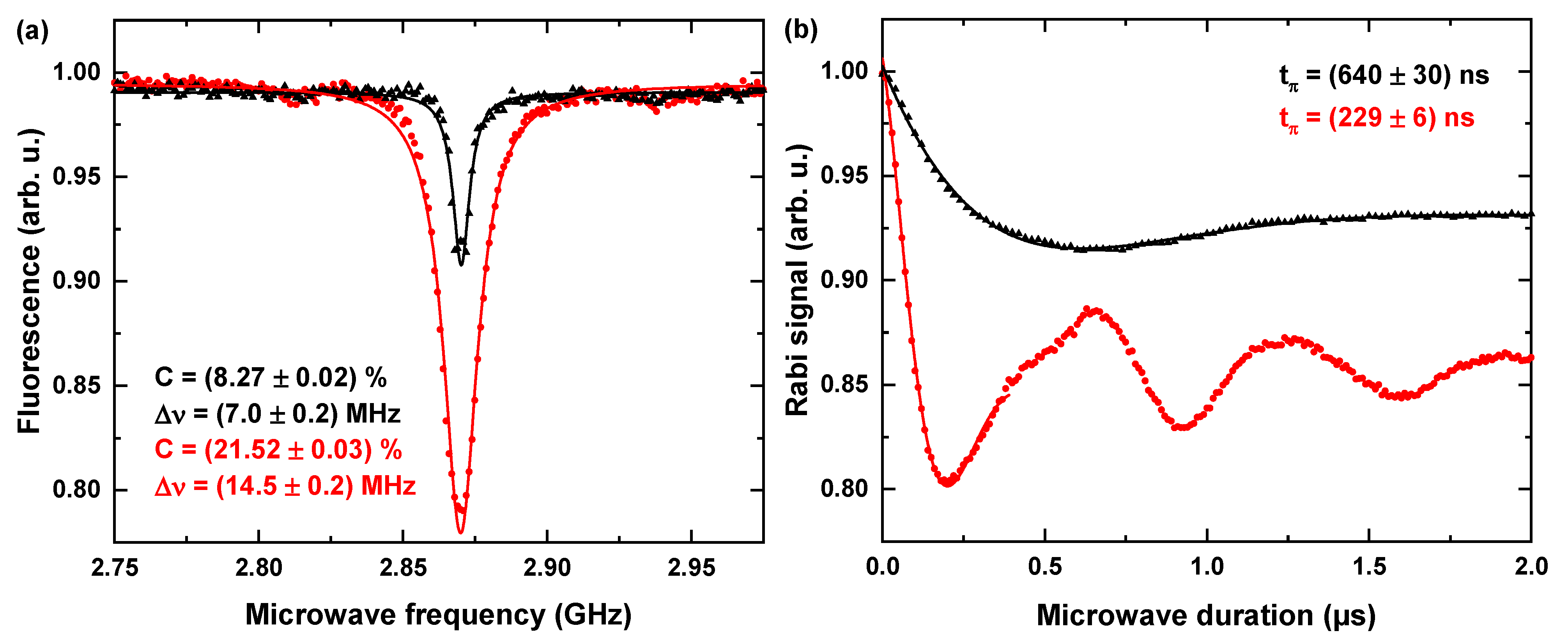
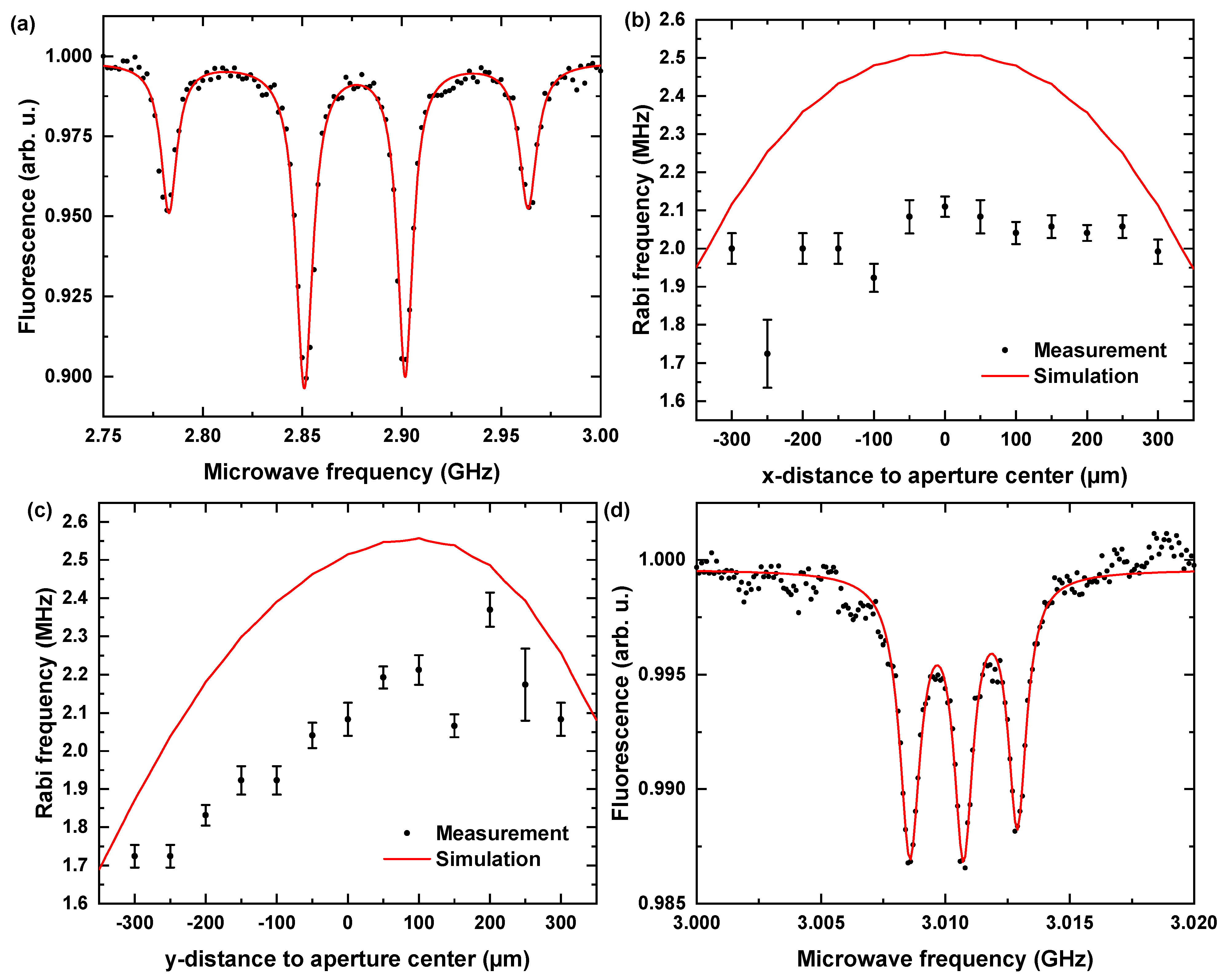
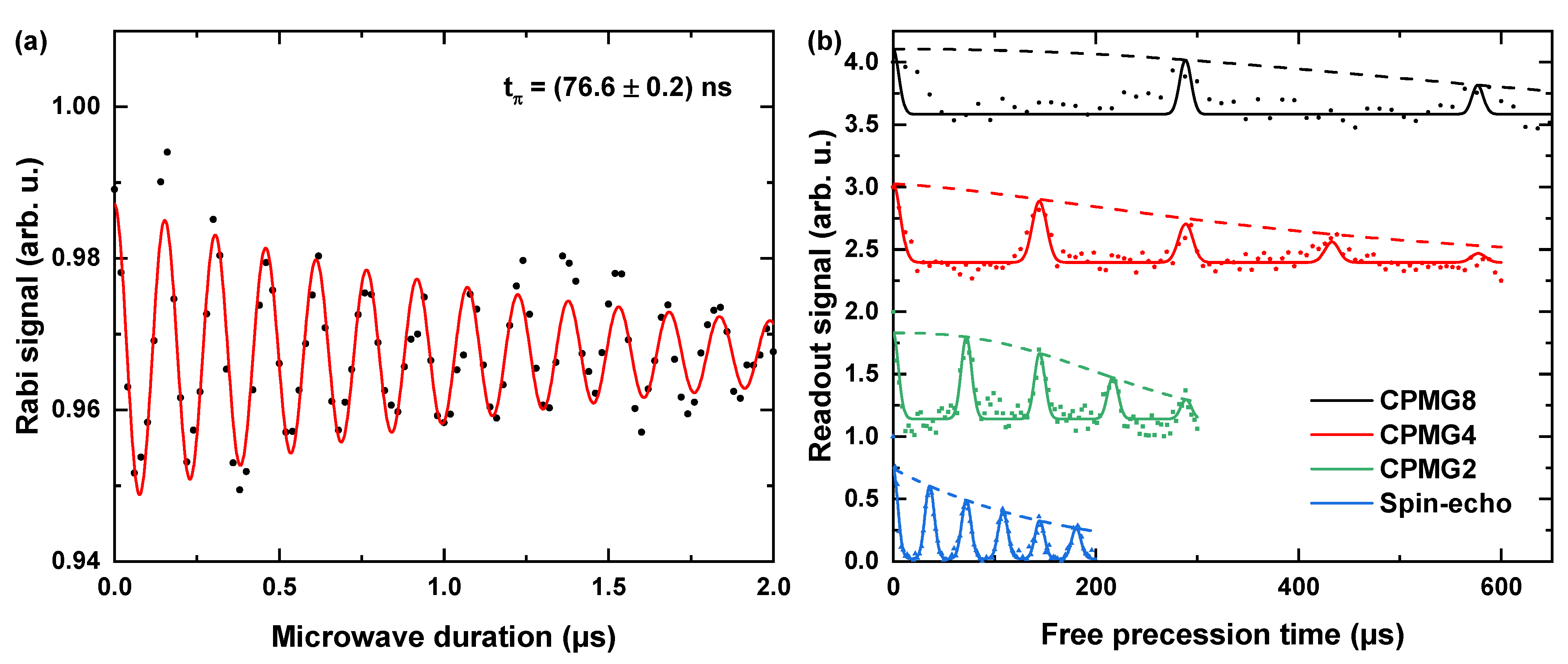
5. Antenna Performance

Comparison—Sputtering and Thermal Evaporation: We investigated the influence of the physical vapor deposition (PVD) method used to deposit the electrically conducting gold layer. For this purpose, we characterized two geometrically identical MW antenna batches, one with a sputtered gold layer the other with a thermally evaporated gold layer. We note that the sputtered gold layer showed superior adhesion compared to the thermally evaporated one.
We performed ODMR and Rabi oscillations without an external magnetic field. The optical excitation power was set to P Opt = 700 μ W and the MW power before amplification (+45 dB) was P MW = −15 dBm. We found that antennas with a thermally evaporated gold layer outperformed antennas with a sputtered layer, as shown in Figure 5a. On average, we determined ODMR contrasts of 10% ± 3% and Ω R of 0.86 ± 0.06 MHz for sputtered antennas; and 21% ± 2% contrast and Ω R of 2.4 MHz ± 0.5 MHz for thermally evaporated ones. The thermally evaporated antennas achieved comparably high contrasts in comparison to highly optimized ODMR experiments (≈30% according to [62,63]). Significant power broadening of the ODMR resonances indicates high MW power driving the NV centers, as displayed in Figure 5b. We attribute this enhancement to a lower power loss within the gold layer due to decreased amounts of impurities and crystal defects created during the sputtering process. Taking into account this finding, we restricted further characterization to thermally evaporated antennas.
Spatial Homogeneity: To evaluate the spatial homogeneity of the radiated MW field, we performed Rabi oscillation measurements ( P Opt = 700 μ W, P MW = −15 dBm) along multiple designated line-cuts in x and y directions (perpendicular/parallel to the gap). For these measurements, we applied an external magnetic field mostly aligned with one of the 111 crystallographic directions, leading to a significant Zeeman splitting for that subset of NV centers [13]. In this situation, ODMR contrast in a non-aligned ensemble intrinsically lowers. For this resonance pair, we observed 4.67% ± 0.06% contrast, which is typical for NV ensembles involving not perfectly aligned bias fields, leading to spin-mixing and charge state instabilities [62,63]. Rabi oscillations were driven typically at a transition frequency of 2.783 GHz, as in Figure 6a corresponding to a bias field strength of B NV = 6.45 mT ± 0.05 mT. Figure 6b,c summarizes the measurements of the spatial homogeneity of the Ω R . Line-cuts perpendicular to the gap reveal constant Ω R within experimental errors. As expected from the simulation results, we observed a slight increase in Ω R with increasing distance from the gap opening. We determined an average value of 2.1 ± 0.1 MHz over all measurement points within 200 μ m distance to the aperture center. Homogeneity and range are in good agreement with our simulation results (compare Figure 4f). We attribute the on average slightly lowered Rabi frequency Ω R to unconsidered losses of our MW circuitry and the potential impedance mismatch of the electrically conducting gluing point for the coaxial connectors. The radiated MW fields’ homogeneity on the scale of the aperture area enables higher coherence times for NV ensembles, leading to enhanced sensitivities. Furthermore, simultaneous MW irradiation of high amplitude within a macroscopic area provides position independent high contrast and therefore an improved signal-to-noise ratio, making this antenna type promising for wide-field [21,22,23,24,25,26,27,28,29,30,31,32,33] and scanning NV-based sensing applications [13,34,35,36,37,38,39,40,41].
Suppression of power broadening-pulsed ODMR: NV-related applications often require one to suppress the power broadening—e.g., when hyperfine transitions of the NV center need to be addressed. Pulsed ODMR schemes instead of continuous driving can suppress power broadening [64]. Here, we show that our antenna also allows for reliable pulsed ODMR measurements. We performed pulsed ODMR using NV centers close to the aperture center. Optical spin initialization and read out at 532 nm were realized with 1 μ s long laser pulses. Resonant spin manipulation involved 2 μ s MW pulses at −30 dBm source MW power amplified by factor of +45 dB. The pulsed ODMR measurement at B NV = 5 mT in Figure 6d reveals the hyperfine interaction of the NV center electronic spin with the 14 N nucleus. We thus confirm the usability of our antennas at low power for efficient, pulsed spin manipulation.
High-Power Applications: High MW powers enable us to realize faster and more complex pulse sequences typically occurring in dynamical decoupling schemes [20]. Dynamically decoupling the NV center from the environmental noise can increase the coherence times, resulting in higher AC magnetic field sensitivities and an increase of the detectable frequency range of AC magnetic fields. Here, we demonstrated dynamical decoupling using spin-echo [14] and Carr Purcell Meiboom Gill (CPMG) pulse sequences [15]. We resonantly drove a transition at 3.01076 GHz corresponding to B NV = 5 mT. Note that we did not observe any significant heating or evident nonlinear effects when applying high-power MW pulses. We observed Ω R in the range of 6 to 10 MHz, depending on the control power amplification (Figure 7a). With the MW power applied in Figure 7a, we realized spin-echo and CPMG pulse sequences with different numbers of π -pulses (1, 2, 4 and 8) (Figure 7b). In comparison to spin-echo, which yielded T 2 = 167.1 μ s, CPMG8 allowed us to increase T 2 up to 638.1 μ s. The antenna is evidently suitable for high-power applications, especially for NV-based AC magnetometry. We infer that our antennas are also usable for advanced spin manipulation techniques based on quantum optimal control theory [65].

6. Conclusions

In this work, we designed and fabricated MW antenna systems for NV-based sensing applications. We optimized a Ω -shaped, microstripline design considering macroscopic spatial homogeneity, wide bandwidth, large amplitudes and ease of implementation with scanning confocal/AFM setups, risk-free sample handling and straightforward fabrication. Our simulations showed that the gap and the radial structure of the antenna govern its resonance properties. A key feature of the design is an aperture with a radius of 300 μ m, defining the homogeneously irradiated area. The design achieves a high bandwidth, along with desirable resonance properties within a macroscopic area with considerably high MW field amplitudes well-suited for NV-based sensing applications. We established a reliable microfabrication process and tested the fabricated MW antennas for typical NV spin manipulation protocols.
We compared sputtering and thermal evaporation for the deposition of the electrically conducting gold layer and found that thermally evaporated layers significantly improve the antenna performance. By mapping the achievable Rabi frequencies within the antenna aperture, we showed the macroscopic homogeneity of the radiated MW field. We tested these antennas in low-power and high-power applications by demonstrating pulsed ODMR measurements and advanced dynamical decoupling protocols. Our antennas can be straightforwardly used in optimized NV sensing approaches, e.g., using optimal control pulses, and in scanning NV magnetometry setups. Consequently, we envisage that our antenna design can add to practical NV sensing.

Author Contributions

E.N. acquired funding. O.R.O., R.N. and E.N. planned the design, fabrication and the process development. O.R.O. and R.N. worked on numerical simulation and optimization. O.R.O. fabricated the antennas. O.R.O. and R.N. performed the characterization experiments. O.R.O. and N.O. performed the application based experiments. R.N. and E.N. supervised the project. O.R.O., N.O. and R.N. wrote the original draft. All the authors contributed during reviewing and editing. All authors have read and agreed to the published version of the manuscript.

Funding

We acknowledge funding via NanoMatFutur grant of the German Ministry of Education and Research (FKZ13N13547). This work has received funding from the European Union’s Horizon 2020 research and innovation program under the Marie Skłodowska-Curie grant agreement N “765267”(QuSCo).

Data Availability Statement

The data presented in this study are available on request from the corresponding author.

Acknowledgments

We would like to acknowledge Uwe Hartmann (Saarland University, Saarbrücken, Germany) for granting access to their cleanroom facilities, especially the sputtering machine; Indujan Sivanesarajah (Saarland University, Saarbrücken, Germany) for his assistance; Günter Marchand (Saarland University, Saarbrücken, Germany) for his help in fabricating the chromium photomask; Robert Strahl (Leibniz Institute for New Materials, Saarbrücken, Germany) for his help with the thermal evaporation; and Dipti Rani for her assistance during prototyping.

Conflicts of Interest

The authors declare no conflict of interest.

References

  1. Jaskula, J.C.; Bauch, E.; Arroyo-Camejo, S.; Lukin, M.D.; Hell, S.W.; Trifonov, A.S.; Walsworth, R.L. Superresolution optical magnetic imaging and spectroscopy using individual electronic spins in diamond. Opt. Express 2017, 25, 11048–11064. [Google Scholar] [CrossRef] [Green Version]
  2. Barson, M.S.; Peddibhotla, P.; Ovartchaiyapong, P.; Ganesan, K.; Taylor, R.L.; Gebert, M.; Mielens, Z.; Koslowski, B.; Simpson, D.A.; McGuinness, L.P.; et al. Nanomechanical sensing using spins in diamond. Nano Lett. 2017, 17, 1496–1503. [Google Scholar] [CrossRef] [Green Version]
  3. Pham, L.M.; DeVience, S.J.; Casola, F.; Lovchinsky, I.; Sushkov, A.O.; Bersin, E.; Lee, J.; Urbach, E.; Cappellaro, P.; Park, H.; et al. NMR technique for determining the depth of shallow nitrogen-vacancy centers in diamond. Phys. Rev. B 2016, 93, 045425. [Google Scholar] [CrossRef] [Green Version]
  4. Arai, K.; Belthangady, C.; Zhang, H.; Bar-Gill, N.; DeVience, S.; Cappellaro, P.; Yacoby, A.; Walsworth, R.L. Fourier magnetic imaging with nanoscale resolution and compressed sensing speed-up using electronic spins in diamond. Nat. Nanotechnol. 2015, 10, 859–864. [Google Scholar] [CrossRef]
  5. Grinolds, M.; Warner, M.; De Greve, K.; Dovzhenko, Y.; Thiel, L.; Walsworth, R.L.; Hong, S.; Maletinsky, P.; Yacoby, A. Subnanometre resolution in three-dimensional magnetic resonance imaging of individual dark spins. Nat. Nanotechnol. 2014, 9, 279–284. [Google Scholar] [CrossRef] [Green Version]
  6. Doherty, M.W.; Struzhkin, V.V.; Simpson, D.A.; McGuinness, L.P.; Meng, Y.; Stacey, A.; Karle, T.J.; Hemley, R.J.; Manson, N.B.; Hollenberg, L.C.; et al. Electronic properties and metrology applications of the diamond NV- center under pressure. Phys. Rev. Lett. 2014, 112, 047601. [Google Scholar] [CrossRef] [PubMed] [Green Version]
  7. Plakhotnik, T.; Doherty, M.W.; Cole, J.H.; Chapman, R.; Manson, N.B. All-optical thermometry and thermal properties of the optically detected spin resonances of the NV–center in nanodiamond. Nano Lett. 2014, 14, 4989–4996. [Google Scholar] [CrossRef] [PubMed] [Green Version]
  8. Kucsko, G.; Maurer, P.C.; Yao, N.Y.; Kubo, M.; Noh, H.J.; Lo, P.K.; Park, H.; Lukin, M.D. Nanometre-scale thermometry in a living cell. Nature 2013, 500, 54–58. [Google Scholar] [CrossRef] [PubMed]
  9. Doherty, M.W.; Manson, N.B.; Delaney, P.; Jelezko, F.; Wrachtrup, J.; Hollenberg, L.C. The nitrogen-vacancy colour centre in diamond. Phys. Rep. 2013, 528, 1–45. [Google Scholar] [CrossRef] [Green Version]
  10. Goldman, M.L.; Doherty, M.; Sipahigil, A.; Yao, N.Y.; Bennett, S.; Manson, N.; Kubanek, A.; Lukin, M.D. State-selective intersystem crossing in nitrogen-vacancy centers. Phys. Rev. B 2015, 91, 165201. [Google Scholar] [CrossRef] [Green Version]
  11. Goldman, M.L.; Sipahigil, A.; Doherty, M.; Yao, N.Y.; Bennett, S.; Markham, M.; Twitchen, D.; Manson, N.; Kubanek, A.; Lukin, M.D. Phonon-induced population dynamics and intersystem crossing in nitrogen-vacancy centers. Phys. Rev. Lett. 2015, 114, 145502. [Google Scholar] [CrossRef] [Green Version]
  12. Barry, J.F.; Schloss, J.M.; Bauch, E.; Turner, M.J.; Hart, C.A.; Pham, L.M.; Walsworth, R.L. Sensitivity optimization for NV-diamond magnetometry. Rev. Mod. Phys. 2020, 92, 015004. [Google Scholar] [CrossRef]
  13. Bernardi, E.; Nelz, R.; Sonusen, S.; Neu, E. Nanoscale sensing using point defects in single-crystal diamond: Recent progress on nitrogen vacancy center-based sensors. Crystals 2017, 7, 124. [Google Scholar] [CrossRef] [Green Version]
  14. Hahn, E.L. Spin echoes. Phys. Rev. 1950, 80, 580. [Google Scholar] [CrossRef]
  15. Carr, H.Y.; Purcell, E.M. Effects of Diffusion on Free Precession in Nuclear Magnetic Resonance Experiments. Phys. Rev. 1954, 94, 630–638. [Google Scholar] [CrossRef]
  16. Gullion, T.; Baker, D.B.; Conradi, M.S. New, compensated carr-purcell sequences. J. Magn. Reson. (1969) 1990, 89, 479–484. [Google Scholar] [CrossRef]
  17. Viola, L.; Lloyd, S. Dynamical suppression of decoherence in two-state quantum systems. Phys. Rev. A 1998, 58, 2733. [Google Scholar] [CrossRef] [Green Version]
  18. Cywiński, Ł.; Lutchyn, R.M.; Nave, C.P.; Sarma, S.D. How to enhance dephasing time in superconducting qubits. Phys. Rev. B 2008, 77, 174509. [Google Scholar] [CrossRef] [Green Version]
  19. Slichter, C.P. Principles of Magnetic Resonance; Springer Science & Business Media: Berlin/Heidelberg, Germany, 2013; Volume 1. [Google Scholar]
  20. Degen, C.L.; Reinhard, F.; Cappellaro, P. Quantum sensing. Rev. Mod. Phys. 2017, 89, 035002. [Google Scholar] [CrossRef] [Green Version]
  21. Turner, M.J.; Langellier, N.; Bainbridge, R.; Walters, D.; Meesala, S.; Babinec, T.M.; Kehayias, P.; Yacoby, A.; Hu, E.; Lončar, M.; et al. Magnetic field fingerprinting of integrated-circuit activity with a quantum diamond microscope. Phys. Rev. Appl. 2020, 14, 014097. [Google Scholar] [CrossRef]
  22. Mizuno, K.; Ishiwata, H.; Masuyama, Y.; Iwasaki, T.; Hatano, M. Simultaneous wide-field imaging of phase and magnitude of AC magnetic signal using diamond quantum magnetometry. Sci. Rep. 2020, 10, 1–10. [Google Scholar] [CrossRef] [PubMed]
  23. Horsley, A.; Appel, P.; Wolters, J.; Achard, J.; Tallaire, A.; Maletinsky, P.; Treutlein, P. Microwave device characterization using a widefield diamond microscope. Phys. Rev. Appl. 2018, 10, 044039. [Google Scholar] [CrossRef] [Green Version]
  24. Glenn, D.R.; Fu, R.R.; Kehayias, P.; Le Sage, D.; Lima, E.A.; Weiss, B.P.; Walsworth, R.L. Micrometer-scale magnetic imaging of geological samples using a quantum diamond microscope. Geochem. Geophys. Geosyst. 2017, 18, 3254–3267. [Google Scholar] [CrossRef]
  25. Simpson, D.A.; Tetienne, J.P.; McCoey, J.M.; Ganesan, K.; Hall, L.T.; Petrou, S.; Scholten, R.E.; Hollenberg, L.C. Magneto-optical imaging of thin magnetic films using spins in diamond. Sci. Rep. 2016, 6, 1–8. [Google Scholar] [CrossRef] [PubMed]
  26. Clevenson, H.; Trusheim, M.E.; Teale, C.; Schröder, T.; Braje, D.; Englund, D. Broadband magnetometry and temperature sensing with a light-trapping diamond waveguide. Nat. Phys. 2015, 11, 393–397. [Google Scholar] [CrossRef] [Green Version]
  27. Nowodzinski, A.; Chipaux, M.; Toraille, L.; Jacques, V.; Roch, J.F.; Debuisschert, T. Nitrogen-vacancy centers in diamond for current imaging at the redistributive layer level of integrated circuits. Microelectron. Reliab. 2015, 55, 1549–1553. [Google Scholar] [CrossRef] [Green Version]
  28. Chipaux, M.; Tallaire, A.; Achard, J.; Pezzagna, S.; Meijer, J.; Jacques, V.; Roch, J.F.; Debuisschert, T. Magnetic imaging with an ensemble of nitrogen-vacancy centers in diamond. Eur. Phys. J. D 2015, 69, 1–10. [Google Scholar] [CrossRef] [Green Version]
  29. Le Sage, D.; Arai, K.; Glenn, D.R.; DeVience, S.J.; Pham, L.M.; Rahn-Lee, L.; Lukin, M.D.; Yacoby, A.; Komeili, A.; Walsworth, R.L. Optical magnetic imaging of living cells. Nature 2013, 496, 486–489. [Google Scholar] [CrossRef] [Green Version]
  30. Steinert, S.; Ziem, F.; Hall, L.; Zappe, A.; Schweikert, M.; Götz, N.; Aird, A.; Balasubramanian, G.; Hollenberg, L.; Wrachtrup, J. Magnetic spin imaging under ambient conditions with sub-cellular resolution. Nat. Commun. 2013, 4, 1–6. [Google Scholar] [CrossRef] [Green Version]
  31. Pham, L.M.; Le Sage, D.; Stanwix, P.L.; Yeung, T.K.; Glenn, D.; Trifonov, A.; Cappellaro, P.; Hemmer, P.R.; Lukin, M.D.; Park, H.; et al. Magnetic field imaging with nitrogen-vacancy ensembles. New J. Phys. 2011, 13, 045021. [Google Scholar] [CrossRef]
  32. Steinert, S.; Dolde, F.; Neumann, P.; Aird, A.; Naydenov, B.; Balasubramanian, G.; Jelezko, F.; Wrachtrup, J. High sensitivity magnetic imaging using an array of spins in diamond. Rev. Sci. Instrum. 2010, 81, 043705. [Google Scholar] [CrossRef] [Green Version]
  33. Maertz, B.; Wijnheijmer, A.; Fuchs, G.; Nowakowski, M.; Awschalom, D. Vector magnetic field microscopy using nitrogen vacancy centers in diamond. Appl. Phys. Lett. 2010, 96, 092504. [Google Scholar] [CrossRef] [Green Version]
  34. Ariyaratne, A.; Bluvstein, D.; Myers, B.A.; Jayich, A.C.B. Nanoscale electrical conductivity imaging using a nitrogen-vacancy center in diamond. Nat. Commun. 2018, 9, 1–7. [Google Scholar] [CrossRef] [Green Version]
  35. Thiel, L.; Rohner, D.; Ganzhorn, M.; Appel, P.; Neu, E.; Müller, B.; Kleiner, R.; Koelle, D.; Maletinsky, P. Quantitative nanoscale vortex imaging using a cryogenic quantum magnetometer. Nat. Nanotechnol. 2016, 11, 677–681. [Google Scholar] [CrossRef] [Green Version]
  36. Pelliccione, M.; Jenkins, A.; Ovartchaiyapong, P.; Reetz, C.; Emmanouilidou, E.; Ni, N.; Jayich, A.C.B. Scanned probe imaging of nanoscale magnetism at cryogenic temperatures with a single-spin quantum sensor. Nat. Nanotechnol. 2016, 11, 700–705. [Google Scholar] [CrossRef]
  37. Appel, P.; Ganzhorn, M.; Neu, E.; Maletinsky, P. Nanoscale microwave imaging with a single electron spin in diamond. New J. Phys. 2015, 17, 112001. [Google Scholar] [CrossRef]
  38. Tetienne, J.P.; Hingant, T.; Kim, J.V.; Diez, L.H.; Adam, J.P.; Garcia, K.; Roch, J.F.; Rohart, S.; Thiaville, A.; Ravelosona, D.; et al. Nanoscale imaging and control of domain-wall hopping with a nitrogen-vacancy center microscope. Science 2014, 344, 1366–1369. [Google Scholar] [CrossRef]
  39. Grinolds, M.S.; Hong, S.; Maletinsky, P.; Luan, L.; Lukin, M.D.; Walsworth, R.L.; Yacoby, A. Nanoscale magnetic imaging of a single electron spin under ambient conditions. Nat. Phys. 2013, 9, 215–219. [Google Scholar] [CrossRef] [Green Version]
  40. Maletinsky, P.; Hong, S.; Grinolds, M.S.; Hausmann, B.; Lukin, M.D.; Walsworth, R.L.; Loncar, M.; Yacoby, A. A robust scanning diamond sensor for nanoscale imaging with single nitrogen-vacancy centres. Nat. Nanotechnol. 2012, 7, 320–324. [Google Scholar] [CrossRef]
  41. Rondin, L.; Tetienne, J.P.; Spinicelli, P.; Dal Savio, C.; Karrai, K.; Dantelle, G.; Thiaville, A.; Rohart, S.; Roch, J.F.; Jacques, V. Nanoscale magnetic field mapping with a single spin scanning probe magnetometer. Appl. Phys. Lett. 2012, 100, 153118. [Google Scholar] [CrossRef] [Green Version]
  42. Yang, L.-L.; Liu, Q.-Q.; Pan, X.-Y.; Chen, D.-M. Design and application of a near field microwave antenna for the spin control of nitrogen-vacancy centers. Chin. Phys. Lett. 2010, 27, 038401. [Google Scholar]
  43. Rudnicki, D.; Mrózek, M.; Młynarczyk, J.; Gawlik, W. Microwave spectroscopy for diagnostics of nitrogen vacancy defects in diamond samples. Photonics Lett. Pol. 2013, 5, 143–145. [Google Scholar] [CrossRef] [Green Version]
  44. Mrózek, M.; Mlynarczyk, J.; Rudnicki, D.S.; Gawlik, W. Circularly polarized microwaves for magnetic resonance study in the GHz range: Application to nitrogen-vacancy in diamonds. Appl. Phys. Lett. 2015, 107, 013505. [Google Scholar] [CrossRef] [Green Version]
  45. Sasaki, K.; Monnai, Y.; Saijo, S.; Fujita, R.; Watanabe, H.; Ishi-Hayase, J.; Itoh, K.M.; Abe, E. Broadband, large-area microwave antenna for optically detected magnetic resonance of nitrogen-vacancy centers in diamond. Rev. Sci. Instrum. 2016, 87, 053904. [Google Scholar] [CrossRef]
  46. Qin, L.; Fu, Y.; Zhang, S.; Zhao, J.; Gao, J.; Yuan, H.; Ma, Z.; Shi, Y.; Liu, J. Near-field microwave radiation function on spin assembly of nitrogen vacancy centers in diamond with copper wire and ring microstrip antennas. Jpn. J. Appl. Phys. 2018, 57, 072201. [Google Scholar] [CrossRef]
  47. Chen, Y.; Guo, H.; Li, W.; Wu, D.; Zhu, Q.; Zhao, B.; Wang, L.; Zhang, Y.; Zhao, R.; Liu, W.; et al. Large-area, tridimensional uniform microwave antenna for quantum sensing based on nitrogen-vacancy centers in diamond. Appl. Phys. Express 2018, 11, 123001. [Google Scholar] [CrossRef]
  48. Dong, M.; Hu, Z.; Liu, Y.; Yang, B.; Wang, Y.; Du, G. A fiber based diamond RF B-field sensor and characterization of a small helical antenna. Appl. Phys. Lett. 2018, 113, 131105. [Google Scholar] [CrossRef] [Green Version]
  49. Soshenko, V.; Rubinas, O.; Vorobyov, V.; Bolshedvorskii, S.; Kapitanova, P.; Sorokin, V.; Akimov, A. Microwave Antenna for Exciting Optically Detected Magnetic Resonance in Diamond NV Centers. Bull. Lebedev Phys. Inst. 2018, 45, 237–240. [Google Scholar] [CrossRef]
  50. Alegre, T.P.M.; Santori, C.; Medeiros-Ribeiro, G.; Beausoleil, R.G. Polarization-selective excitation of nitrogen vacancy centers in diamond. Phys. Rev. B 2007, 76, 165205. [Google Scholar] [CrossRef] [Green Version]
  51. Bayat, K.; Choy, J.; Farrokh Baroughi, M.; Meesala, S.; Loncar, M. Efficient, uniform, and large area microwave magnetic coupling to NV centers in diamond using double split-ring resonators. Nano Lett. 2014, 14, 1208–1213. [Google Scholar] [CrossRef]
  52. Herrmann, J.; Appleton, M.A.; Sasaki, K.; Monnai, Y.; Teraji, T.; Itoh, K.M.; Abe, E. Polarization-and frequency-tunable microwave circuit for selective excitation of nitrogen-vacancy spins in diamond. Appl. Phys. Lett. 2016, 109, 183111. [Google Scholar] [CrossRef]
  53. Zhang, N.; Zhang, C.; Xu, L.; Ding, M.; Quan, W.; Tang, Z.; Yuan, H. Microwave magnetic field coupling with nitrogen-vacancy center ensembles in diamond with high homogeneity. Appl. Magn. Reson. 2016, 47, 589–599. [Google Scholar] [CrossRef]
  54. Yang, X.; Zhang, N.; Yuan, H.; Bian, G.; Fan, P.; Li, M. Microstrip-line resonator with broadband, circularly polarized, uniform microwave field for nitrogen vacancy center ensembles in diamond. AIP Adv. 2019, 9, 075213. [Google Scholar] [CrossRef] [Green Version]
  55. Mariani, G.; Nomoto, S.; Kashiwaya, S.; Nomura, S. System for the remote control and imaging of MW fields for spin manipulation in NV centers in diamond. Sci. Rep. 2020, 10, 1–10. [Google Scholar] [CrossRef]
  56. Yaroshenko, V.; Soshenko, V.; Vorobyov, V.; Bolshedvorskii, S.; Nenasheva, E.; Kotel’nikov, I.; Akimov, A.; Kapitanova, P. Circularly polarized microwave antenna for nitrogen vacancy centers in diamond. Rev. Sci. Instrum. 2020, 91, 035003. [Google Scholar] [CrossRef]
  57. Horowitz, V.R.; Alemán, B.J.; Christle, D.J.; Cleland, A.N.; Awschalom, D.D. Electron spin resonance of nitrogen-vacancy centers in optically trapped nanodiamonds. Proc. Natl. Acad. Sci. USA 2012, 109, 13493–13497. [Google Scholar] [CrossRef] [Green Version]
  58. Weiland, T. A discretization model for the solution of Maxwell’s equations for six-component fields. Arch. Elektron. Uebertrag. 1977, 31, 116–120. [Google Scholar]
  59. Jelezko, F.; Gaebel, T.; Popa, I.; Gruber, A.; Wrachtrup, J. Observation of Coherent Oscillations in a Single Electron Spin. Phys. Rev. Lett. 2004, 92, 076401. [Google Scholar] [CrossRef]
  60. Gruber, A.; Dräbenstedt, A.; Tietz, C.; Fleury, L.; Wrachtrup, J.; Borczyskowski, C.V. Scanning Confocal Optical Microscopy and Magnetic Resonance on Single Defect Centers. Science 1997, 276, 2012–2014. [Google Scholar] [CrossRef] [Green Version]
  61. MacQuarrie, E.R.; Gosavi, T.A.; Bhave, S.A.; Fuchs, G.D. Continuous dynamical decoupling of a single diamond nitrogen-vacancy center spin with a mechanical resonator. Phys. Rev. B 2015, 92, 224419. [Google Scholar] [CrossRef] [Green Version]
  62. Mizuno, K.; Nakajima, M.; Ishiwata, H.; Hatano, M.; Iwasaki, T. Electron spin contrast of high-density and perfectly aligned nitrogen-vacancy centers synthesized by chemical vapor deposition. Appl. Phys. Express 2021, 14, 032001. [Google Scholar] [CrossRef]
  63. Osterkamp, C.; Mangold, M.; Lang, J.; Balasubramanian, P.; Teraji, T.; Naydenov, B.; Jelezko, F. Engineering preferentially-aligned nitrogen-vacancy centre ensembles in CVD grown diamond. Sci. Rep. 2019, 9, 1–7. [Google Scholar] [CrossRef] [PubMed]
  64. Dréau, A.; Lesik, M.; Rondin, L.; Spinicelli, P.; Arcizet, O.; Roch, J.F.; Jacques, V. Avoiding power broadening in optically detected magnetic resonance of single NV defects for enhanced dc magnetic field sensitivity. Phys. Rev. B 2011, 84, 195204. [Google Scholar] [CrossRef] [Green Version]
  65. Rembold, P.; Oshnik, N.; Müller, M.M.; Montangero, S.; Calarco, T.; Neu, E. Introduction to quantum optimal control for quantum sensing with nitrogen-vacancy centers in diamond. AVS Quantum Sci. 2020, 2, 024701. [Google Scholar] [CrossRef]
Figure 1. (a) A schematic representation of the Ω -shaped antenna and its implementation in a confocal microscope utilizing a piezo scanner (coaxial connector design by avitek, coaxial cable design by Steven Minichiello and objective design by thorfynn; source: https://grabcad.com accessed on 7 June 2021). (b) A schematic representation of the geometry of the Ω -shaped antenna design (note that the scale bar is approximate and the sketch does not give the exact geometry of the simulated antenna but illustrates the design in general). Microwave (MW) modes enter and leave the calculation domain via the waveguide ports indicated in red. Inset: Simulated MW radiation pattern. Here, strong directivity towards the sample is visible.
Nanomaterials 11 02108 g001
Figure 2. Process flow for Omega antennas. The color key: grey—glass substrate; blue—chromium; yellow—gold; green—adhesion promoter; red—photoresist; black—photomask; violet—UV-illumination.
Nanomaterials 11 02108 g002
Figure 3. (a) Achievable MW amplitude for different inner radius values r w . Points from different simulation runs. (b) Calculation of the frequency-dependent S 11 parameter (back reflection coefficient) with a ground plane for the 50 μ m thick diamond (solid black) and the 300 μ m thick diamond (solid red) and without the ground plane (dashed lines). (c) MW amplitude and Rabi frequency dependence on the distance to the antenna top surface. Rabi frequencies Ω R were determined for a resonantly driven transition of the subset of nitrogen vacancy (NV) centers aligned in 111 crystallographic direction. Input MW power equals 1 W.
Nanomaterials 11 02108 g003
Figure 4. Field simulation results for a 50 μ m thick electronic grade diamond (ac) and for a 300 μ m thick IIa diamond (df). All field data were taken 10 nm below the diamond sample’s top surface and correspond to a MW input power of 1 W. (a,b,d,e) Field distribution of the MW in x and y directions. (c,f) 2D maps of theoretically expected Rabi frequencies Ω R for a resonantly driven transition of the subset of nitrogen vacancy (NV) centers aligned in 111 crystallographic direction. The dashed circle marks the circumference of the aperture. Insets: detailed views of the aperture areas.
Nanomaterials 11 02108 g004
Figure 5. Comparison between sputtered and evaporated layers. The evaporated antennas show better performance in terms of radiated MW amplitude, as shown by the increased optically detected magnetic resonance (ODMR) contrast C ((a), 8% vs. 22%), and Rabi frequency Ω R ((b), 800 kHz vs. 2.2 MHz, t π = π -pulse duration). Note that the ODMR resonance of the evaporated antenna is strongly power broadened ( Δ ν = FWHM). Points indicate the experimentally obtained data and solid curve denotes fits used to obtain the mentioned parameters.
Nanomaterials 11 02108 g005
Figure 6. (a) Continuous ODMR measurements of an NV ensemble with an externally applied magnetic field. For the outermost resonance pair, a splitting of 181 MHz ± 1 MHz with high contrast (4.67% ± 0.06% at −15 dBm source MW power) was obtained. For the corresponding subset of NV centers, we determined a projection of the magnetic field on the NV axis of 6.45 mT ± 0.05 mT. (b,c) Characterization of the homogeneity of the radiated MW field amplitude perpendicular and parallel to the gap. While the amplitude parallel to the gap slightly depended on the distance to the gap, as expected, the amplitude perpendicular to the gap remained unaffected, showing that the full area of the aperture is reliably usable for spin manipulation protocols. (d) Pulsed ODMR of one of the resonances showing the hyperfine transitions due to 14 N nuclear spin coupling. The black points indicate the experimentally obtained data, solid black lines indicate the error bars and the solid red lines indicate either fits or simulated data.
Nanomaterials 11 02108 g006
Figure 7. (a) Typical Rabi oscillation measurements, which are primarily used to obtain relevant pulse parameter to be used in multi-pulse sensing schemes. The measurement performed at Ω R 6.5 MHz. (b) Spin-echo and Carr Purcell Meiboom Gill (CPMG)-n measurements with the NV ensemble performed with the pulse parameters obtained from (a). The plots have been fit and scaled along the y-axis for comparison. The points show the experimentally obtained data, solid curves denote the fit and the dashed lines indicate the fit envelopes. The spin-echo measurements reveal T 2 167 μ s. Applying CPMG-8 pulse sequences leads to almost a fourfold improvement in the decoherence time of the spin state. From the fit, the calculated enhanced decoherence times for the CPMG-2/4/8 protocols were ≈245 μ s/≈425 μ s/≈638 μ s, respectively.
Nanomaterials 11 02108 g007
Publisher’s Note: MDPI stays neutral with regard to jurisdictional claims in published maps and institutional affiliations.

