
A Brief Overview of Electrochromic Materials and Related Devices: A Nanostructured Materials Perspective


 ,
,
Abstract
:1. Introduction
- -
- “Smart Windows”;
- -
- Displays;
- -
- Reflective blinds;
- -
- Variable reflection mirrors;
- -
- Sensors.
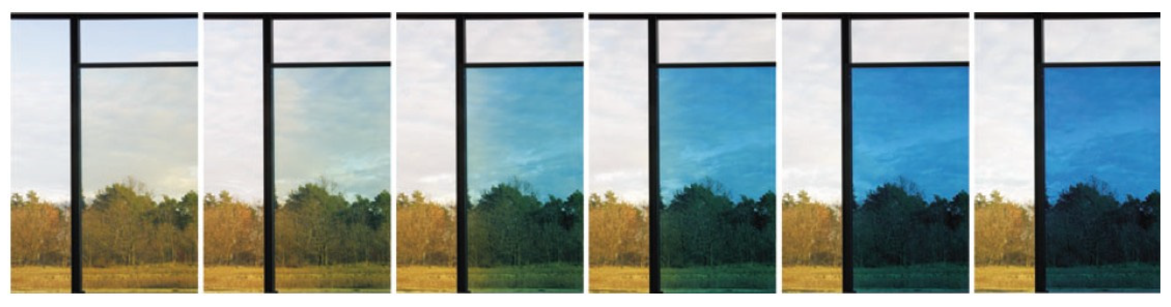
2. “Smart Windows”
- -
- electric energy is required only during mode switching;
- -
- low activation voltage (1–5 V);
- -
- a wide variety of “Smart Window” tints (blue, grey, brown, etc.);
- -
- in the bleached state, electrochromic devices have a transparency level of 50–70%, in the colored state—10–25%.
3. Electrochromism and Electrochromic Materials: Classification and Applications
- -
- Control of energy transfer in different environments, for example, filtering solar radiation using “Smart Window” devices [25,26,27]. Fast mode switching (colored/bleached) is not required, but the device should be capable of filtering both visible and near-infrared radiation. Moreover, the transparency of the window packages must be at least 70%.
- -
- -
- Mirror light modulators [7], for example, antiglare mirrors for cars. Fast mode switching and high transparency are not required.
3.1. Classification of Electrochromic Materials
- (1)
- Type I EC materials, such as viologen, heptyl, etc., are soluble in both their reduced and oxidized states.
- (2)
- Type II EC materials are soluble in their colorless redox state but form a solid film on the electrode surface.
- (3)
- Type III EC materials are solids in both redox states, and they form an insoluble film on the electrode surface. Type III materials include groups IV, V transition metal oxides (TMO), conductive polymers, Prussian blue and metal polymers. Three types of mechanism for changing color/transparency (according to I. F. Chang) are presented in Figure 5.
3.2. Organic EC
3.3. Transition Metal Oxides
3.4. WO3 Electrochromic Films

4. ECD (Electrochromic Device) Structure
4.1. Substrate
4.2. Transparent Conductive Electrode
4.3. Electrochromic Layer
4.4. Electrolyte (Ion Conductor)
- -
- compatibility with anodic and cathodic materials;
- -
- high ionic conductivity;
- -
- no electron transfer between electrochromic layers;
- -
- high transparency without scattering effect.
4.5. Counter Electrode
5. WO3 Film Fabrication
5.1. Electrochemical Deposition
5.2. Sol–Gel
- (1)
- hydrolysis with the formation of reactive M–OH groups:
- (2)
- condensation resulting in bridge oxygen formation:
5.3. Spray Pyrolysis
5.4. Magnetron Sputtering
6. Nanomaterials for Electrochromic Devices
7. Conclusions
- (1)
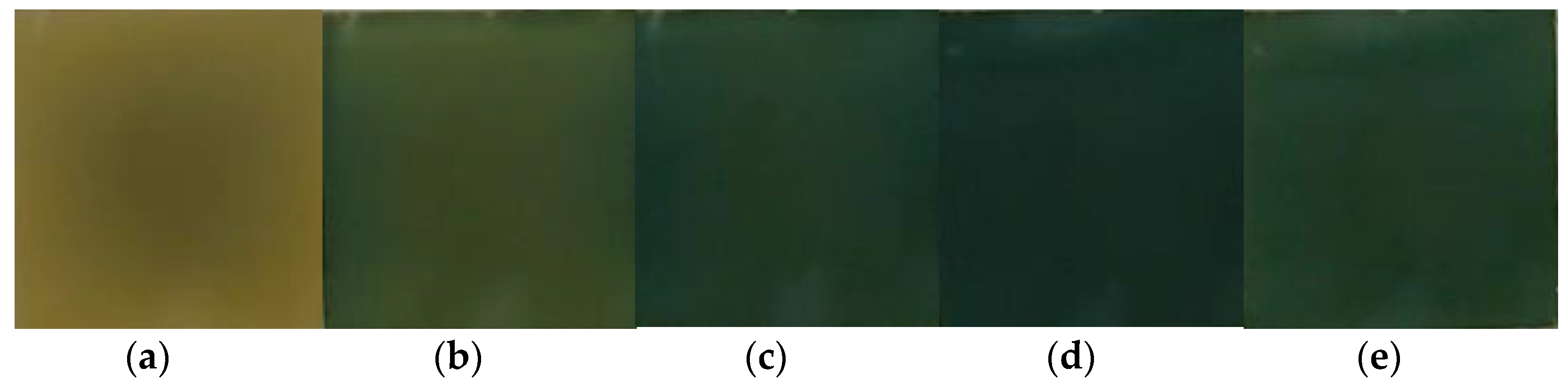
- There are several hypotheses concerning the mechanism of electrochromism in WO3. Generally, the electrochromic effect in WO3 films can be described as an electrochemical cathodic polarization during which H+ ions are transferred from the electrolyte and an electron is transferred from the ITO electrode. As a result, WO3 film switches from a bleached to a colored state; its color varies from pale blue to dark blue and black. The conductivity of WO3 films is determined by the presence of cations (H+, Li+, etc.) and electrons. As already mentioned, the coloration mechanism in WO3 films has still been insufficiently investigated.
- (2)
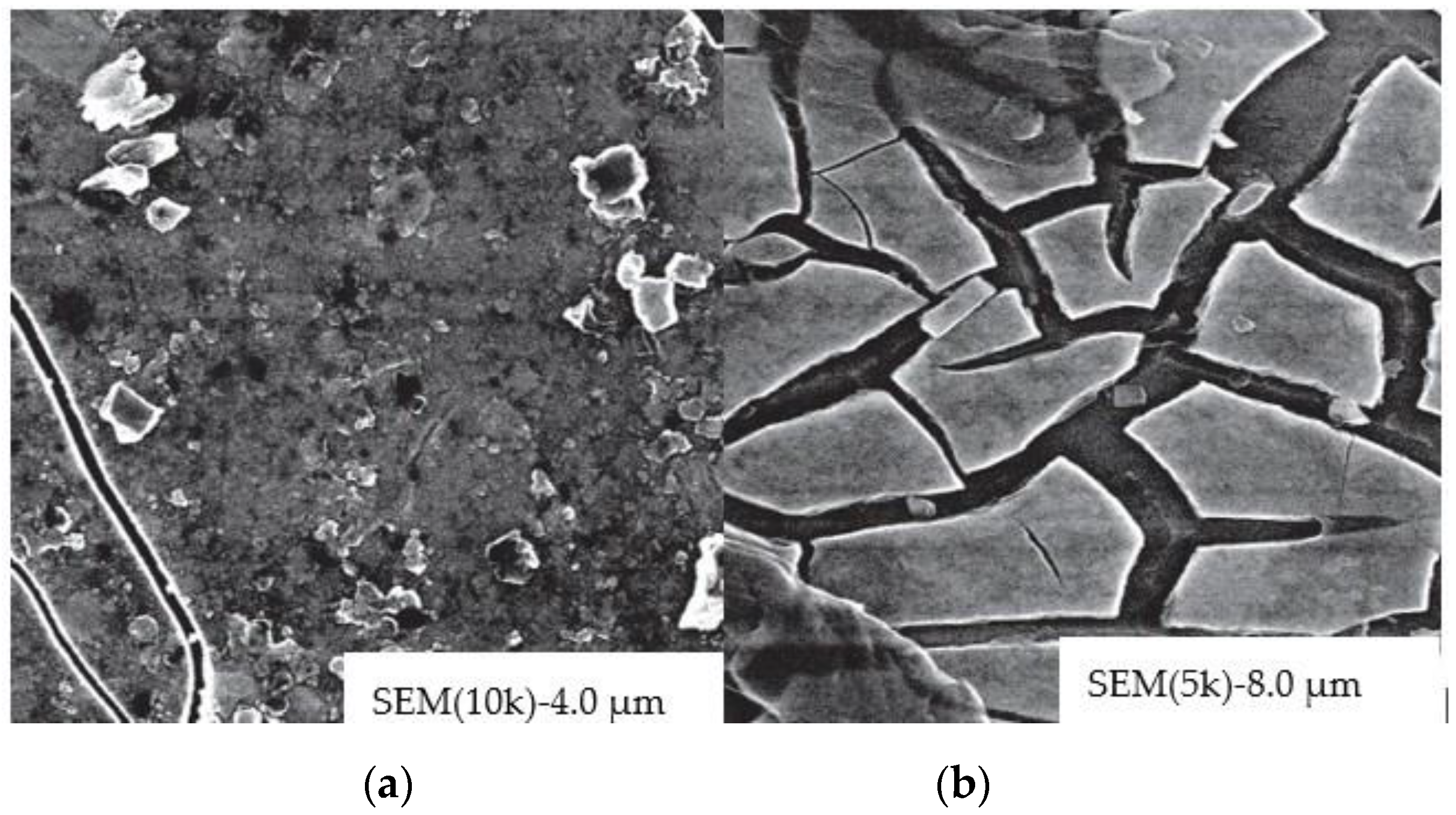
- Despite a large number of works devoted to the study of electrochromic WO3 films, the influence of the structural state on optical properties during the electrochemical reaction has not been fully investigated. Different film deposition techniques have been proposed. Film morphology is dependent on deposition technique and can be amorphous, crystalline, nanocrystalline or hybrid. Additionally, there is still a constant need for new technologies to produce WO3 films, and nanostructured WO3 films in particular. Therefore, there is a necessity to study the fabrication of amorphous, crystalline and nanocrystalline WO3 films, including their GO/rGO modification. Analysis of literary sources makes it possible to identify prospects for the development of WO3/rGO fabrication technologies. The obtained data will be useful in the development of WO3 fabrication technologies.
Author Contributions
Funding
Institutional Review Board Statement
Informed Consent Statement
Data Availability Statement
Conflicts of Interest
Abbreviations
| EC | electrochromic materials; |
| PhC | photochromic materials; |
| ThC | thermochromic materials; |
| GhC | gasochromic materials; |
| PDLC | polymer-dispersed liquid crystals; |
| LDC | liquid crystal dispersions; |
| ECD | electrochromic devices; |
| ECW | electrochromic windows; |
| TMO | transition metal oxides; |
| GO | graphene oxide; |
| rGO | reduced graphene oxide; |
| SPD | suspended particles; |
| EMR | electromagnetic radiation. |
References
- Addington, D.M.; Schodek, D.L. Smart Materials and New Technologies for the Architecture and Design Professions; Elsevier Science: Oxford, UK, 2005; p. 241. [Google Scholar]
- Granqvist, C.G.; Green, S.; Niklasson, G.A.; Mlyuka, N.R.; Kraemer, S.; Georén, P. Advance in chromogenic materials and devices. Thin Solid Film. 2010, 518, 3046–3053. [Google Scholar] [CrossRef]
- Bamfield, P. Chromic Phenomena the Technological Applications of Colour Chemistry; Royal society of Chemistry (RSC): Cambridge, UK, 2001; p. 374. [Google Scholar]
- Baetens, R.; Jelle, B.P.; Gustavsen, A. Properties, requirements and possibilities of smart windows for dynamic daylight and solar energy control in buildings: A state-of-the art review. Sol. Energy Mater. Sol. Cells 2010, 94, 87–105. [Google Scholar] [CrossRef] [Green Version]
- Aoul, K.T.; Attoye, D.; Al Ghatrif, L. Perfomance of electrochromic glazing: State of the art review. In 4th International Conference on Civil Engineering and Materials Science (ICCEMS 2019), Proceedings of the IOP Conference Series Materials Science and Engineering, Bangkok, Thailand, 17–19 May 2019; IOP Publishing: Bristol, UK, 2019; Volume 603, p. 22085. [Google Scholar] [CrossRef] [Green Version]
- Pacheco-Torgal, F.; Rasmussen, E.; Granqvist, C.-G.; Ivanov, V.; Kaklauskas, A.; Makonin, S. Start-Up Creation: The Smart Eco-Efficient Built Environment; Woodhead Publishing: Sawston, UK, 2016; p. 510. [Google Scholar] [CrossRef]
- Somani, P.R.; Radhakrishman, S. Electrochromic materials and devices: Present and future. Mater. Chem. Phys. 2002, 77, 117–133. [Google Scholar] [CrossRef]
- Aburas, M.; Soebarto, V.; Williamson, T.; Liang, R.; Ebendorff-Heidepriem, H.; Wu, Y. Thermochromic smart window technologies for building application: A review. Appl. Energy 2019, 255, 113522. [Google Scholar] [CrossRef]
- Wittwer, V.; Datz, M.; Ell, J.; Georg, A.; Graf, W.; Walze, G. Gasochromic windows. Sol. Energy Mater. Sol. Cells 2004, 84, 305–314. [Google Scholar] [CrossRef]
- Zhao, Y.; Ikeda, T. Smart Light-Responsive Materials: Azobenze-Containing Polymers and Liquid Crystals; John Wiley & Sons: Hoboken, NJ, USA, 2009; p. 514. [Google Scholar] [CrossRef]
- Lampert, C.M. Chromogenic smart materials. Mater. Today 2004, 7, 28–35. [Google Scholar] [CrossRef]
- Granqvist, C.G.; Lansaker, P.C.; Mlyuka, N.R.; Niklasson, G.A.; Avendano, E. Progress in chromogenics: New results for electrochromic and thermochromic materials and devices. Sol. Energy Mater. Sol. Cells 2009, 93, 2032–2039. [Google Scholar] [CrossRef]
- Rauh, R.D.; Wang, F.; Reynolds, J.R.; Mecker, D.L. High coloration efficiency electrochromics and their application to multi-color devices. Electrochim. Acta 2001, 46, 2023–2029. [Google Scholar] [CrossRef]
- Svensson, J.S.E.M.; Granqvist, C.G. Electrochromic coatings for “Smart Windows”. Sol. Energy Mater. 1985, 12, 391–402. [Google Scholar] [CrossRef]
- Clayton, R.P. Introduction to Electromagnetic Compatibility; John Wiley & Sons: Hoboken, NJ, USA, 2006; p. 1013. [Google Scholar]
- Lampert, C.M. Large-area smart glass and integrated photovoltaics. Sol. Energy Mater. Sol. Cells 2003, 76, 489–499. [Google Scholar] [CrossRef]
- Deb, S.K. A novel electrophotographic system. Appl. Opt. 1969, 8, 192–195. [Google Scholar] [CrossRef]
- Deb, S.K. Optical and photoelectric properties and colour centres in thin films of tungsten oxide. Philos. Mag. 1973, 27, 801–822. [Google Scholar] [CrossRef]
- Gao, W.; Lee, S.H.; Bullock, J.; Xu, Y.; Benson, D.K.; Morrison, S.; Branz, H.M. Photovoltaic-powered monolithic tandem electrochromic smart window device. Sol. Energy Mater. Sol. Cells. 1999, 59, 243–254. [Google Scholar] [CrossRef]
- Niklasson, G.A.; Berggren, L.; Jonsson, A.K.; Ahuja, R.; Skorodumova, N.V.; Backholm, J.; Stromme, M. Electrochemical studies of the electron states of disordered electrochromic oxides. Sol. Energy Mater. Sol. Cells 2006, 90, 385–394. [Google Scholar] [CrossRef]
- Beaujuge, P.M.; Reynolds, J.R. Color control in π-conjugated organic polymers for use in electrochromic devices. Chem. Rev. 2010, 110, 268–320. [Google Scholar] [CrossRef]
- Ferara, M.; Bengisu, M. Materials that Change Color—Smart Materials Intelligent Design; Springer: Berlin/Heidelberg, Germany, 2014; p. 145. [Google Scholar] [CrossRef]
- Kraft, A. Electrochromism: A fascinating branch of electrochemistry. ChemText 2019, 5, 1–18. [Google Scholar] [CrossRef]
- Pettersson, H.; Gruszecki, T.; Johansson, L.-H.; Edwards, M.O.M.; Hagfeldt, A.; Matuszczyk, T. Direct-driven electrochromic displays based on nanocrystalline electrodes. Displays 2004, 25, 223–230. [Google Scholar] [CrossRef]
- Murphy, M.; Gustavsen, A.; Jelle, B.P.; Haase, M. Energy savings potential with electrochromic switchable glazing. In Proceedings of the 9th Nordic Symposium on Building Physics, Tampere, Finland, 29 May–2 June 2011; Volume 3, pp. 1281–1288. [Google Scholar]
- Lampert, C.M. Electrochromic materials and devices for energy efficient windows. Sol. Energy Mater. 1984, 11, 1–27. [Google Scholar] [CrossRef] [Green Version]
- Rauh, R.D. Electrochromic windows: An overview. Electrochim. Acta 1999, 44, 3165–3176. [Google Scholar] [CrossRef]
- Mortimer, R.J. Organic electrochromic materials. Electrochim. Acta 1999, 44, 2971–2981. [Google Scholar] [CrossRef]
- Mortimer, R.J. Electrochromic materials. Annu. Rev. Mater. Res. 2011, 41, 241–268. [Google Scholar] [CrossRef]
- Rowley, N.M.; Mortimer, R.J. New electrochromic materials. Sci. Prog. 2002, 85, 243–262. [Google Scholar] [CrossRef]
- Granqvist, C.G.; Pehlivan, I.B.; Green, S.V.; Lansaker, P.C.; Niklasson, G.A. Oxide-based electrochromics: Advances in materials and devices. Mater Res. Soc. Symp. Proc. 2011, 1328, 11–22. [Google Scholar] [CrossRef]
- Granqvist, C.G. Handbook of Inorganic Electrochromic Materials; Elsevier Science: Amsterdam, The Netherlands, 1995; p. 650. [Google Scholar]
- Argum, A.A.; Aubert, P.-H.; Thompson, B.C.; Scwebdeman, I.; Gaupp, C.L.; Hwang, J.; Pinto, H.J.; Tanner, D.B.; MacDiarmid, A.G.; Reynolds, J.R. Multicolored electrochromism in polymers structures and devices. Chem. Mater. 2004, 16, 4401–4412. [Google Scholar] [CrossRef] [Green Version]
- Jelle, B.P.; Hagen, G.; ØdegÅrd, R. Transmission spectra of an electrochromic window based on Polyaniline, Tungsten Oxide and a solid polymer electrolyte. Electrochim. Acta 1992, 37, 1377–1380. [Google Scholar] [CrossRef]
- Chang, I.F. Electrochromic and electrochemichromic materials and phenomena. In Nonemissive Electooptic Displays; Springer: New York, NY, USA, 1976; pp. 155–196. [Google Scholar] [CrossRef]
- Chang, I.F.; Gilbert, B.L.; Sun, T.I. Electrochemichromic systems for display applications. J. Electrochem. Soc. 1975, 122, 955–962. [Google Scholar] [CrossRef]
- Zou, Y.S.; Zhang, Y.C.; Lou, D.; Wang, H.P.; Gu, L.; Dong, Y.H.; Dou, K.; Song, X.F.; Zeng, H.B. Structural and optical properties of WO3 films deposited by pulsed laser deposition. J. Alloy. Compd. 2014, 583, 465–470. [Google Scholar] [CrossRef]
- Zhang, G.; Lu, K.; Zhang, X.; Yuan, W.; Shi, M.; Ning, H.; Tao, R.; Liu, X.; Yao, R.; Peng, J. Effects of annealing temperature on optical band gap of sol-gel tungsten trioxide films. Micromachines 2018, 9, 377. [Google Scholar] [CrossRef] [Green Version]
- Bohnke, O.; Bohnke, C.; Robert, G. Electrochromism in WO3 thin films. I. LiClO4-Propylene Carbonate—Water electrolyres. Solid State Ion. 1982; 6, 121–128. [Google Scholar] [CrossRef]
- Wei, C.; He, J.; Dettelbach, K.E.; Johnson, N.J.J.; Sherbo, R.S.; Berlinguette, C.P. Photodeposited amorphous oxide films for electrochromic windows. Chem 2018, 4, 821–832. [Google Scholar] [CrossRef] [Green Version]
- Saxena, A.P.; Deepa, M.; Joshi, A.G.; Bhandari, S.; Srivastava, A.K. Poly(3,4-ethylenedioxythiophene)-Ionic Liquid Functionalized Graphene/Reduced Graphene Oxide Nanostructures: Improved Conduction and Electrochromism. ACS Appl. Mater. Interfaces 2011, 3, 1115–1126. [Google Scholar] [CrossRef] [PubMed]
- Bange, K. Colouration of tungsten oxide films: A model for optically active coatings. Sol. Energy Mater. Sol. Cells 1999, 58, 1–131. [Google Scholar] [CrossRef]
- Granqvist, C.G. Electrochromic tungsten oxide films: Review of progress. Sol. Energy Mater. Sol. Cells 2000, 60, 201–262. [Google Scholar] [CrossRef]
- Callister, W.D.; Rethwisch, D.G. Materials Science and Engineering—An Introduction; John Wiley & Sons Inc.: Hoboken, NJ, USA, 2019; p. 1000. [Google Scholar]
- Monk, P.M.S. The Viologens: Physicochemical Properties, Synthesis and Applications of the Salts of 4,4′-Bipyrindine; Wiley: Chichester, UK, 1998; p. 332. [Google Scholar]
- Grant, B.; Clecak, N.J.; Oxsen, M.; Jaffe, A.; Keller, G.S. Study of the electrochromism of methoxyflurene compounds. J. Org. Chem. 1980, 45, 702–705. [Google Scholar] [CrossRef]
- Rosseinsky, D.R.; Monk, P.M.S.; Hann, R.A. Anion-dependent aqueous electrodeposition of electrochromic 1,1′-bis-cyanophenyl-4,4′-bipyridilium (cyanophenylparaquat) radical cation by cyclic voltammetry amd spectrochemical studies. Electrochim. Acta 1990, 35, 1113–1123. [Google Scholar] [CrossRef]
- Rosseinsky, D.R.; Monk, P.M.S. Electrochromic cyanophenylparaquat (CPQ: 1,1′-bis-cayanophenyl-4,4′-bipyridilium) studied voltammetrically, spectroelectrochemically and by ESR. Sol. Energy Mater. Sol. Cells 1992, 25, 201–210. [Google Scholar] [CrossRef]
- Kanagarj, M.; Velayutham, D.; Suryanarayanan, V.; Kathiresan, M.; Ho, K.-C. Viologen based electrochromic materials and devices. J. Mater. Chem. C 2019, 7, 4622–4637. [Google Scholar] [CrossRef]
- Gadgil, B.; Damlin, P.; Heinonen, M.; Kvarnström, C. A facile one step electrostatically driven electrodeposition of polyviologen-reduced grapheme oxide nanocomposite films for enhanced electrochromic performance. Carbon 2015, 89, 53–62. [Google Scholar] [CrossRef]
- Chudov, K.A.; Levchenko, K.S.; Poroshin, N.O.; Shmelin, P.S.; Grebennikov, E.P.; Shchegol’kov, A.V. Synthesis and properties of new Electrochromic derivatives of 3-aryl-4,5-bis(pyridine-4-yl) oxazole. Russ. Chem. Bull. 2019, 68, 1565–1569. [Google Scholar] [CrossRef]
- Grimsdale, A.C.; Chan, K.L.; Martin, R.E.; Jokisz, P.G.; Holmes, A.B. Synthesis of Light-Emitting Conjugated Polymers for Applications in Electroluminescent Devices. Chem. Rev. 2009, 109, 897–1091. [Google Scholar] [CrossRef] [PubMed]
- Brabec, C.; Dyakanov, V.; Scherf, U. Organic photovoltaics. Energy Environ. Sci. 2009, 2, 251–261. [Google Scholar] [CrossRef]
- Sapp, S.; Sotzing, G.A.; Reynolds, J.R. High contrast ratio and fast –switching dual polymer electrochromic devices. Chem. Mater. 1998, 10, 2101–2108. [Google Scholar] [CrossRef]
- Jenekhe, S.A.; Kiserow, D.J. Chromogenic effects in polymers: An overview of the driverse ways of tuning optical properties in real time. In 230th ACS National Meeting, Proceedings of the American Chemical Society Symposium Series, Washington, DC, USA, 28 August–1 September 2005; American Chemical Society: Washington, DC, USA, 2005; Volume 888, p. 2. [Google Scholar] [CrossRef] [Green Version]
- Beaujuge, P.M.; Ellinger, S.; Reynolds, J.R. Spray processable green to highly transmissive electrochromics via chemically polymerizable donor-acceptor heterocyclic pentamers. Adv. Mater. 2008, 20, 2772–2776. [Google Scholar] [CrossRef]
- Dyer, A.L.; Thompson, E.J.; Reynolds, J.R. Completing the Color Palette with Spray-Processable Polymer Electrochromics. ACS Appl. Mater. Interface 2011, 3, 1787–1795. [Google Scholar] [CrossRef]
- Thakur, V.K.; Ding, G.; Ma, J.; Lee, P.S.; Lu, X. Hybrid materials and polymer electrolytes for electrochromic device applications. Adv. Mater. 2012, 24, 4071–4096. [Google Scholar] [CrossRef] [PubMed]
- Monk, P.M.S.; Mortimer, R.J.; Rosseinsky, D.R. Electrochromism: Fundamentals and Applications; VCH: Weinheim, Germany, 1995; p. 243. [Google Scholar] [CrossRef]
- Wen, R.; Niklasson, G.; Granqvist, C. Electrochromic Iridium oxide films: Compatibility with propionic acid, potassium hydroxide, and lithium perchlorate in propylene carbonate. Sol. Energy Mater. Sol. Cells 2013, 120 Pt A, 151–156. [Google Scholar] [CrossRef] [Green Version]
- Lin, S.-Y.; Wang, C.-M.; Kao, K.-S.; Chen, Y.-C.; Liu, C.-C. Electrochromic properties of MoO3 thin films derived by a sol-gel process. J. Sol-Gel Sci. Technol. 2010; 53, 51–58. [Google Scholar] [CrossRef]
- Korošec, R.C.; Bukovec, P. Sol-Gel Prepared NiO Thin Films for Electrochromic Applications. Acta Chim. Slov. 2006, 53, 136–147. [Google Scholar]
- Zelazowska, E.; Rysiakiewicz-Pasek, E. Thin TiO2 films for an electrochromic system. Opt. Mater. 2009, 31, 1802–1804. [Google Scholar] [CrossRef]
- Wei, Y.; Zhou, J.; Zheng, J.; Xu, C. Improved stability of electrochromic devices using Ti-doped V2O5 film. Electrochica Acta 2015, 166, 277–284. [Google Scholar] [CrossRef]
- Westphal, T.M.; Cholant, C.M.; Azevedo, C.F.; Moura, E.A.; Silva, D.L.; Lemos, R.M.J.; Pawlicka, A.; Gundel, A.; Flores, W.H.; Avellaneda, C.O. Influence of the Nb2O5 doping on the electrochemical properties of V2O5 thin films. J. Electroanal. Chem. 2017, 790, 50–56. [Google Scholar] [CrossRef]
- Mansouri, M.; Mahmoodi, T. Ab Initio Investigation on the Effect of Transition Metals Doping and Vacancies in WO3. Acta Phys. Pol. 2016, 129, 8–13. [Google Scholar] [CrossRef]
- Ashrit, P. Transition Metal Oxide Thin Film-Based Chromogenics and Devices; Elsevier: Amsterdam, The Netherlands, 2017; p. 376. [Google Scholar]
- Zhang, J.-G.; Benson, D.K.; Tracy, C.E.; Deb, S.K.; Czanderna, A.W.; Bechinger, C. Chromic Mechanism in Amorphous WO3 Films. In Proceedings of the 190th Electrochemical Society Meeting, San Antonio, TX, USA, 11–13 February 1996; pp. 1–19. [Google Scholar]
- Wang, Z.; Chen, G.; Zhang, H.; Liang, L.; Gao, J.; Cao, H. In situ TEM investigation of hexagonal WO3 irreversible transformation to Li2WOScr. Material 2021, 203, 114090. [Google Scholar] [CrossRef]
- Baloukas, B.; Martinu, L. WO3/SiO2 composite optical films for the fabrication of electrochromic interference filters. Appl. Opt. 2012, 51, 3346–3356. [Google Scholar] [CrossRef] [PubMed]
- Mukherjee, R.; Sahay, P.P. Effect of precursors on the microstructural, optical, electrical and electrochromic properties of WO3 nanocrystalline thin films. J. Mater. Sci. Mater. Electron. 2015, 26, 6293–6305. [Google Scholar] [CrossRef]
- Lusis, A.; Kleperis, J.; Pentjuss, E. Model of electrochromic and related phenomena in tungsten oxide thin films. J. Solid State Electrochem. 2003, 7, 106–112. [Google Scholar] [CrossRef]
- Khyzhun, O.Y.; Solonin, Y.M. Electronic structure of nanoparticles of substoichometric hexagonal tungsten oxides. In Proceedings of the International Conference on Nanoscience and Technology, Basel, Switzerland, 30 July–4 August 2007; Volume 61, pp. 534–539. [Google Scholar] [CrossRef]
- Gabrusenoks, J.V.; Cikmach, P.D.; Lusis, A.R.; Kleperis, J.J.; Ramans, G.M. Electrochromic colour centres in amorphous tungsten trioxide then films. Solid State Ion. 1984, 14, 25–30. [Google Scholar] [CrossRef]
- Temmink, A.; Anderson, O.; Bange, K.; Hantsche, H.; Yu, X. Optical absorption of amorphous WO3 and binding state of tungsten. Thin Solid Film. 1990, 192, 211–218. [Google Scholar] [CrossRef]
- Niklasson, G.A.; Granqvist, C.G. Electrochromic for smart window: Thin films of tungsten oxide and nickel oxide, and devices based on these. J. Mater. Chem. 2007, 17, 127–156. [Google Scholar] [CrossRef] [Green Version]
- Shchegolkov, A.V.; Shchegolkov, A.V. Electrochromic nanostructure WO3 films prepared by electrochemical deposition: Receipt and properties. Perspekt. Mater. 2020, 1, 54–63. [Google Scholar] [CrossRef]
- Pehlivan, I.B. Functionalization of Polymer Electrolytes for Electrochromic Windows; Acta Univ. Upsliensis: Uppsala, Sweden, 2013; p. 174. [Google Scholar]
- Rojas-Gonzalez, E.A.; Niklasson, G.A. Coloration of tungsten oxide electrochromic thin films at high bias potentials and low intercalation levels. Mater. Lett. X 2020, 7, 100048. [Google Scholar] [CrossRef]
- Vijayakumar, E.; Yun, Y.-H.; Quy, V.H.V.; Lee, Y.-H.; Kang, S.-H.; Ahn, K.-S.; Lee, S.W. Development of tungsten trioxide using pulse and continuous electrodeposition and its properties in electrochromic devices. J. Electrochem. Soc. 2019, 166, 86–92. [Google Scholar] [CrossRef]
- Kotok, V.; Kovalenko, V.; Solovov, V.; Zima, O.; Nikolenko, M. Some aspects of the WO3 films electrodeposition for application in electrochromic devices. In Proceedings of the 11th International Students Scientific Conference, “Trans-Mech-Art-Chem” Radom, Poland, 17–20 October 2017. [Google Scholar]
- Yoo, S.J.; Lim, J.W.; Sung, Y.-E.; Jung, Y.H.; Choi, H.G.; Kim, D.K. Fast switchable electrochromic properties of tungsten oxide nanowire bundles. Appl. Phys. Lett. 2007, 90, 173126. [Google Scholar] [CrossRef]
- Kondalkar, V.V.; Mali, S.S.; Kharade, R.R.; Khot, K.V.; Patil, P.B.; Mane, R.M.; Choudhury, S.; Patilm, P.S.; Hong, C.K.; Kim, J.H.; et al. High perfoming smart electrochromic device based on honeycomb nanostructured h-WO3 thin films: Hydrothermal assisted synthesis. Dalton Trans. 2015, 44, 2788–2800. [Google Scholar] [CrossRef] [PubMed]
- Kwong, W.L.; Savvides, N.; Sorrell, C.C. Electrodeposited nanostructured WO3 thin films for photoelectrochemical applications. Electrochim. Acta 2012, 75, 371–380. [Google Scholar] [CrossRef]
- Zhu, T.; Chong, M.N.; Chang, E.S. Nanostructured Tungsten Trioxide Thin Films Synthesized for Photoelectrocatalytic Water Oxidation: A review. ChemSusChem Rev. 2014, 7, 2974–2997. [Google Scholar] [CrossRef] [PubMed]
- More, A.J.; Patil, R.S.; Dalavi, D.S.; Mali, S.S.; Hong, C.K.; Gang, M.G.; Kim, J.H.; Patil, P.S. Electrodeposition of nano-granular tungsten oxide thin films for smart window application. Mater. Lett. 2014, 134, 298–301. [Google Scholar] [CrossRef]
- Wang, K.; Zhang, H.; Chen, G.; Tian, T.; Tao, K.; Liang, L. Long-term-stable WO3-PB complementary electrochromic devices. J. Alloy. Compd. 2021, 861, 158534. [Google Scholar] [CrossRef]
- Zheng, R.; Wang, Y.; Pan, J.; Malik, H.A.; Zhang, H.; Jia, C.; Weng, X.; Xie, J.; Deng, L. Towards Easy-to-assemble, Large Area Smart Windows: All-in-one Cross-Linked Electrochromic Material and Device. ACS Appl. Mater. Interfaces 2020, 12, 27526–27536. [Google Scholar] [CrossRef]
- Cai, G.; Wang, J.; Lee, P.S. Next-generation multifunctional electrochromic devices. Acc. Chem. Res. 2016, 49, 1469–1476. [Google Scholar] [CrossRef]
- Granqvist, C.G. Transparent conductors as solar energy materials: A panoramic review. Sol. Energy Material. Sol. Cells. 2007, 91, 1529–1598. [Google Scholar] [CrossRef]
- Mecerreyes, D.; Marcilla, R.; Ochoteco, E.; Grande, H.; Pomposo, J.A.; Vergaz, R.; Pena, J.M.S. A simplified all-polymer flexible electrochromic device. Electrochim. Acta 2004, 49, 3555–3559. [Google Scholar] [CrossRef]
- Gillaspie, D.-T.; Tenent, R.C.; Dillon, A.C. Metal-oxide films for electrochromic applications: Present technology and future directions. J. Mater. Chem. 2010, 20, 9585–9592. [Google Scholar] [CrossRef]
- Edwards, P.P.; Porch, A.; Jones, M.O.; Morgan, D.V.; Perks, R.M. Basic materials physics of transparent conducting oxides. Dalton Trans 2004, 19, 2995–3002. [Google Scholar] [CrossRef]
- Voronin, A.S.; Ivanchenko, F.S.; Simunin, M.M.; Shiverskiy, A.V.; Aleksandrovsky, A.S.; Nemtsev, I.V.; Fadeev, Y.V.; Karpova, D.V.; Khartov, S.V. High performance hybrid rGO/Ag quasi-periodic mesh transparent electrodes for flexible electrochromic devices. Appl. Surf. Sci. 2015, 364, 931–937. [Google Scholar] [CrossRef]
- Li, H.; Elezzabi, A.Y. Simultaneously enabling dynamic transparency control and electrical energy storage via electrochromism. Nanoscale Horiz. 2020, 5, 691–695. [Google Scholar] [CrossRef]
- Lv, H.; Yang, S.; Li, C.; Han, C.; Tang, Y.; Li, X.; Wang, W.; Li, H.; Zhi, C. Suppressing passivation layer of Al anode aqueous electrolytes by complexation of H2PO4- to Al3+ and an electrochromic Al ion battery. Energy Stor. Mater. 2021, 39, 412–418. [Google Scholar] [CrossRef]
- Barbosa, P.C.; Silva, M.M.; Smith, M.J.; Goncalves, A.; Fortunato, E. Studies of solid-state electrochromic devices based on PEO/siliceous hybrids doped with lithium perchlorate. Electrochim. Acta. 2007, 52, 2938–2943. [Google Scholar] [CrossRef] [Green Version]
- Park, S.-I.; Quan, Y.-J.; Kim, S.-H.; Kim, H.; Kim, S.; Chun, D.-M.; Lee, C.S.; Taya, M.; Chu, W.-S.; Ahn, S.-H. A Review on Fabrication Processes for Electrochromic Devices. Int. J. Precis. Eng. Manuf.-Green Technol. 2016; 3, 397–421. [Google Scholar] [CrossRef]
- Jain, N.K.; Sawant, M.S.; Nikam, S.H.; Jhavar, S. Metal deposition: Plasma-based processes. In Encyclopedia of Plasma Technology, 1st ed.; Taylor and Francis: New York, NY, USA, 2016; pp. 722–740. [Google Scholar] [CrossRef]
- Subrahmanyam, A.; Karuppasamy, A. Optical and electrochromic properties of oxygen sputtered tungsten oxide (WO3) thin films. Sol. Energy Mater. Sol. Cells 2007, 91, 266–274. [Google Scholar] [CrossRef]
- Hepel, M.; Redmond, H. Large cation model of dissociative reduction of electrochromic WO3−x films. Cent. Eur. J. Chem. 2009, 7, 234–245. [Google Scholar] [CrossRef]
- Zhou, K.; Wang, H.; Liu, J. Coloration and Ion Insertion Kinetics Study in Electrochromic WO3 Films by Chronoamperometry. Int. J. Electrochem. Sci. 2020, 15, 7821–7832. [Google Scholar] [CrossRef]
- Kwong, W.K.; Qiu, H.; Nakaruk, A.; Koshy, P.; Sorrel, C.C. Photoelectrochemical Properties of WO3 Thin Films Prepared by Electrodeposition. Energy Procedia 2013, 34, 617. [Google Scholar] [CrossRef] [Green Version]
- Velevska, J.; Stojanov, N.; Pecovska-Gjorgevich, M.; Najdoski, M. Electrochromism in tungsten oxide thin films prepared by chemical bath deposition. J. Electrochem. Sci. Eng. 2017, 7, 27. [Google Scholar] [CrossRef]
- Pauporte, T. A simplified Method for WO3 Electrodeposition. J. Electrochem. Soc. 2002, 149, 539–545. [Google Scholar] [CrossRef]
- Arakaki, J.; Reyes, R.; Horn, M.; Estrada, W. Electrochromism in NiOx and WOx obtained by spray pyrolysis. Sol. Energy Mater. Sol. Cells 1995, 37, 33–41. [Google Scholar] [CrossRef]
- Deepa, M.; Srivastava, A.K.; Kar, M.; Agnihotry, S.A. A case study of optical properties and structure of sol-gel derived nanocrystalline electrochromic WO3 films. J. Phys. D Appl. Phys. 2006, 39, 1885–1893. [Google Scholar] [CrossRef]
- Solarska, R.; Alexander, B.D.; Augustynski, J. Electrochromic and structural characteristics of mesoporous WO3 films prepared by a sol-gel method. J. Solid State Electrochem. 2004, 8, 748–756. [Google Scholar] [CrossRef]
- Valyukh, I.; Green, S.; Arwin, H.; Niklasson, G.A.; Wackelgard, E.; Granqvist, C.G. Spectroscopic ellipsometry characterization of electrochromic tungsten oxide and nickel oxide thin films made by sputter deposition. Sol. Energy Mater. Sol. Cells 2010, 94, 724–732. [Google Scholar] [CrossRef] [Green Version]
- Yamada, Y.; Tabata, K.; Yashima, T. The character of WO3 film prepared with RF sputtering. Sol. Energy Mater. Sol. Cells 2007, 91, 29–37. [Google Scholar] [CrossRef]
- Atak, G.; Pehlivan, I.B.; Montero, J.; Granqvist, C.G.; Niklasson, G.A. Electrochromic tungsten oxide films prepared by sputtering: Optimizing cycling durability by judicious choice of deposition parameters. Electrochim. Acta 2021, 367, 137233. [Google Scholar] [CrossRef]
- Qiu, D.; Ji, H.; Zhang, X.; Zhang, H.; Cao, H.; Chen, G.; Tian, T.; Chen, C.; Guo, X.; Liang, L.; et al. Electrochromism of nanocrystal-in-glass tungsten oxide thin films under various conduction cations. Inorg. Chem. 2019, 58, 2089–2098. [Google Scholar] [CrossRef]
- Evecan, D.; Zayim, E. Highly uniform electrochromic tungsten oxide thin films deposite be e-beam evaporation for energy saving systems. Curr. Appl. Phys. 2019, 19, 198–203. [Google Scholar] [CrossRef]
- Vernardou, D.; Psifis, K.; Louloudakis, D.; Papadimitropoulos, G.; Davazoglou, D.; Katsarakis, N.; Koudoumas, E. Low Pressure CVD of Electrochromic WO3 at 400 °C. J. Electrochem. Soc. 2015, 162, 579–582. [Google Scholar] [CrossRef]
- Kraft, A.; Rottman, M. Properties, performance and current status of the laminated electrochromic glass of gesimat. Sol. Energy Mater. Sol. Cells 2009, 93, 2088–2092. [Google Scholar] [CrossRef]
- Brinker, C.; Scherer, G. Sol-Gel Science: The Physics and Chemistry of Sol-Gel Processing; Academic Press, Inc.: Cambridge, MA, USA, 1990; p. 908. [Google Scholar]
- Lenormand, P.; Rieu, M.; Julbe, M.; Castilio, A.; Ansart, S.; Ansart, F. Potentialities of the sol-gel route to develop cathode and electrolyte thick: Application to SOFC systems. Surf. Coat. Technol. 2008, 203, 901–904. [Google Scholar] [CrossRef] [Green Version]
- Agrawal, A.; Cronin, J.P.; Zhang, R. Review of solid-state electrochromic coatings produced using sol-gel techniques. Sol. Energy Mater. Sol. Cells 1993, 31, 9–21. [Google Scholar] [CrossRef]
- Cronin, J.P.; Tarico, D.J.; Tonazzi, J.C.L.; Agrawal, A.; Kennedy, S.R. Microstructure and properties of sol-gel deposited WO3 coatings for large-area electrochromic windows. Sol. Energy Mater. Sol. Cells 1993, 28, 371–386. [Google Scholar] [CrossRef]
- Mujawar, S.; Inamdar, A.; Korosec, C.; Patil, R.C.; Patil, P. Electrochromism in Composite WO3-Nb2O5 Thin Films Synthesized by Spray Pyrolysis Technique. J. Appl. Electrochem. 2011, 41, 397–421. [Google Scholar] [CrossRef]
- Bertus, L.; Enesca, A.; Duta, A. Influence of spray pyrolysis deposition parameters on the optoelectronic properties of WO3 thin films. Thin Solid Film. 2012, 520, 4282–4290. [Google Scholar] [CrossRef]
- Patil, C.; Tarwal, N.; Jadhav, P.; Shinde, P.; Deshmukh, H. Electrochromic Performance of the Mixed V2O5-WO3 Thin Films Synthezed by Pulsed Spray Pyrolysis Technique. Curr. Appl. Phys. 2014, 14, 389–395. [Google Scholar] [CrossRef]
- Bathe, S.R.; Patil, P.S. Electrochromic characteristics of pulsed spray pyrolyzed polycrystalline WO3 thin films. Smart Mater. Struct. 2009, 18, 1–7. [Google Scholar] [CrossRef]
- Kelly, P.; Bradley, J. Pulsed magnetron sputtering-process overview and applications. J. Optoelectron. Adv. Mater. 2009, 11, 1101–1107. [Google Scholar]
- Chen, H.-C.; Jan, D.-J.; Chen, C.-H. Investigation of optical and electrochromic properties of tungsten oxide deposited with horizontal DC and DC pulse magnetron sputtering. Jpn. J. Appl. Phys. 2012, 51, 45503. [Google Scholar] [CrossRef]
- Chen, H.-C.; Chen, D.-J.; Huang, K.-T. Bond and Electrochromic Properties of WO3 Films Deposited with Horizontal DC, Pulsed DC, and RF Sputtering. Electrochim. Acta 2013, 93, 307–313. [Google Scholar] [CrossRef]
- Zhi, M.; Shi, Q.; Wang, M.; Wang, Q. Sol-gel fabrication WO3/rGO nanocomposite film with enhanced electrochromic performance. RSC Adv. 2016, 6, 67488–67494. [Google Scholar] [CrossRef]
- Wang, J.M.; Khoo, E.; Lee, P.S.; Ma, J. Controlled synthesis of WO3 nanorod and their electrochromic properties in H2SO4 electrolyte. J. Phys. Chem. C 2009, 113, 9655–9658. [Google Scholar] [CrossRef]
- Lee, S.-H.; Deshpande, R.; Parilla, P.A.; Jones, K.M.; To, B.; Mahan, A.H.; Dillon, A.C. Crystalline WO3 nanoparticles for highly improved electrochromic applications. Adv. Mater. 2006, 18, 763–766. [Google Scholar] [CrossRef]
- Dinh, N.N.; Hinh, D.H.; Thao, T.T.; Vo-Van, T. Mixed Nanostructured Ti-W Oxides Filsms for Efficient Electrochromic Windows. J. Nanomater. 2012, 2012, 1–7. [Google Scholar] [CrossRef]
- Niu, J.; Wang, Y.; Zou, X.; Tan, Y.; Jia, C.; Weng, X.; Deng, L. Infrared electrochromic materials, devices and applications. Appl. Mater. Today, 2021; 24, 1–27. [Google Scholar] [CrossRef]
- Costa, C.; Pinheiro, C.; Henriques, I.; Laia, C.A.T. Inkjet Printing of Sol-Gel Synthesized Hydrated Tungsten Oxide Nanoparticles for Flexible Electrochromic Devices. Appl. Mater. Interfaces 2012, 4, 1330–1340. [Google Scholar] [CrossRef] [PubMed]
- Luo, J.; Zeng, Q.; Long, Y.; Wang, Y. Preparation of Nano-Polycrystalline WO3 Thin Films and Their Solid-State Electrochromic Display Devices. J. Nanosci. Nanotechnol. 2013, 13, 1372–1376. [Google Scholar] [CrossRef]
- Llordés, A.; Garcia, G.; Gazquez, J.; Milliron, D.J. Tunnable near-infrared and visible-light transmittance in nanocrystal-in-glass composites. Nature 2013, 500, 323–326. [Google Scholar] [CrossRef]
- Shchegolkov, A.V.; Knyazeva, L.G.; Shchegolkov, A.V.; Komarov, F.F.; Parfimovich, I.D. The study of electrochromic films WO3(GO) obtained by electrochemical deposition: Optical and electromagnetic properties. Mendeleev J. Russ. Chem. Soc. 2020, LXIV, 55–62. [Google Scholar]
- Zhao, Q.; Yasi, F.; Qiao, K.; Wei, W.; Yao, Y.; Gao, Y. Printing of WO3/ITO nanocomposite electrochromic smart windows. Sol. Energy Mater Sol. Cells 2019, 194, 95–102. [Google Scholar] [CrossRef]
- Yao, Y.; Zhao, Q.; Wei, W.; Chen, Z.; Zhu, Y.; Zhang, P.; Zhang, Z.; Gao, Y. WO3 quantum-dots electrochromism. Nano Energy 2020, 68, 104350. [Google Scholar] [CrossRef]
- Xiong, S.; Yin, S.; Wang, Y.; Kong, Z.; Lan, J.; Zhang, R.; Gong, M.; Wu, B.; Chu, J.; Wang, X. Organic/inorganic electrochromic nanocomposites with various interfacial interactions: A review. Mater. Sci. Eng. B 2017, 221, 41–53. [Google Scholar] [CrossRef]


| Technology | Energy Efficiency, W/m2 | Energy Saving, W/m2 (Energy Saving in Building) | Transparency, % | Modulation Time, s | Cost, (c.u./m2) |
|---|---|---|---|---|---|
| ECW | + | + | + | – | – |
| SPD | – | – | + | + | + |
| PDLC | – | – | + | + | + |
| LCD | – | – | + | + | + |
| EC Class | Chemical Name | Application | Ref. |
|---|---|---|---|
| Organic | |||
| Conductive polymers | PEDOT (where EDOT = C6H6O2S), PPy (where Py = Pyrrole = C4H5N), PT (where T = thiophene = C4H4S), PANI (where ANI = aniline = C6H4S) | “Smart Windows”, displays | [13,33] |
| Viologens | 3-aryl-4,5-bis (pyridine-4-yl) isoxazole derivatives | Antiglare mirrors and displays | [21,28] |
| Transition metals and lanthanoids | poly [RuII(vbpy)2(py)2]Cl2 (being py = pyridine = C5H5N) | Smart mirrors | [26,30] |
| Metal phthalocyanines (Pc) | [Lu(Pc)2] being Pc = C32H18N8 et al. | Displays | [7,30] |
| Inorganic | |||
| Transition metal oxides (TMOs) | WO3, MoO3, V2O5, TiO2 Nb2O5, Ir(OH)3, NiO et al. | “Smart Windows”, antiglare mirrors | [32,34] |
| Prussian blue (PB) | Prussian blue (C18Fe7N18), Prussian brown (C6Fe2N6), Prussian green (C3FeN3), Prussian white (C6Fe3N6) | “Smart Windows”, displays | [7,29] |
| EC Type | EC Material | Electrochromic Reaction Mechanism | Application | Ref. |
|---|---|---|---|---|
| I (solution) |
| MV2+ + e−(bleached)↔MV+●(colored) | Night vision systems, mirrors | [37,38] |
| II (hybrid) |
| CPQ2+ + e− + X−↔[CPQ+●X−] | Electrochromic paper, “Smart Window” | [39,40,41] |
| III (battery-powered) |
| MOy + x(H+ + e−)↔HxMOy(colored) | “Smart Window” (Boeing 757), Electro-chromic paper | [32,42,43] |
| Organic EC | ||||||
|---|---|---|---|---|---|---|
| State | PANI | P3MPy | MEPA | P3MT | PPY | PT |
| Neutral |  |  |  |  |  |  |
| Oxidized |  |  |  |  |  |  |
| Inorganic EC | ||||||||||||
|---|---|---|---|---|---|---|---|---|---|---|---|---|
| State | WO3 | NiO | NiO/WO3 | |||||||||
| Oxidized |  |  |  |  |  |  |  |  |  |  |  |  |
| Reduction |  |  |  |  |  |  |  |  |  |  |  |  |
| Metal Oxide | Electrochemical Reaction | Color Change | Reaction Type |
|---|---|---|---|
| Manganese oxide (II) | Yellow ↔ brown | A | |
| Cobalt oxide (II) | Green ↔ light blue | A | |
| Nickel oxide (II) | Colorless ↔ brown | A | |
| Molybdenum oxide (VI) | Colorless ↔ blue | C | |
| Vanadium oxide (V) | (A) (C) | Blue ↔ brown (A) Yellow ↔ light blue (C) | C/A |
| Cerium oxide (IV) | Yellow ↔ transparent | C | |
| Niobium oxide (V) | Colorless ↔ light blue | C | |
| Ruthenium oxide (IV) | Blue ↔ brown/yellow | C | |
| Indium oxide (ITO) | Colorless ↔ light blue | C | |
| Iridium oxide (III) | Colorless ↔ blue/grey | C | |
| Tungsten oxide (VI) | Colorless ↔ blue/black | C |
| Technology Types | Scalability | Equipment Cost | Process Costs | Coating Uniformity |
|---|---|---|---|---|
| Electrochemical | +/− | + | + | +/− |
| Chemical | +/− | + | + | − |
| Physical | + | − | − | + |
Publisher’s Note: MDPI stays neutral with regard to jurisdictional claims in published maps and institutional affiliations. |
© 2021 by the authors. Licensee MDPI, Basel, Switzerland. This article is an open access article distributed under the terms and conditions of the Creative Commons Attribution (CC BY) license (https://creativecommons.org/licenses/by/4.0/).
Share and Cite
Shchegolkov, A.V.; Jang, S.-H.; Shchegolkov, A.V.; Rodionov, Y.V.; Sukhova, A.O.; Lipkin, M.S. A Brief Overview of Electrochromic Materials and Related Devices: A Nanostructured Materials Perspective. Nanomaterials 2021, 11, 2376. https://doi.org/10.3390/nano11092376
Shchegolkov AV, Jang S-H, Shchegolkov AV, Rodionov YV, Sukhova AO, Lipkin MS. A Brief Overview of Electrochromic Materials and Related Devices: A Nanostructured Materials Perspective. Nanomaterials. 2021; 11(9):2376. https://doi.org/10.3390/nano11092376
Chicago/Turabian StyleShchegolkov, Aleksei Viktorovich, Sung-Hwan Jang, Alexandr Viktorovich Shchegolkov, Yuri Viktorovich Rodionov, Anna Olegovna Sukhova, and Mikhail Semenovich Lipkin. 2021. "A Brief Overview of Electrochromic Materials and Related Devices: A Nanostructured Materials Perspective" Nanomaterials 11, no. 9: 2376. https://doi.org/10.3390/nano11092376
APA StyleShchegolkov, A. V., Jang, S.-H., Shchegolkov, A. V., Rodionov, Y. V., Sukhova, A. O., & Lipkin, M. S. (2021). A Brief Overview of Electrochromic Materials and Related Devices: A Nanostructured Materials Perspective. Nanomaterials, 11(9), 2376. https://doi.org/10.3390/nano11092376