Abstract
Constant advance in improving the luminous efficacy (ηL) of nitride-based light-emitting diodes (LEDs) plays a critical role for saving measurable amounts of energy. Further development is motivated to approach the efficiency limit for this material system while reducing the costs. In this work, strategies of using thin AlN prebuffer and transitional-refraction-index patterned sapphire substrate (TPSS) were proposed, which pushed up the efficiency of white LEDs (WLEDs). The AlN prebuffer was obtained through physical vapor deposition (PVD) method and TPSS was fabricated by dry-etched periodic silica arrays covered on sapphire. Devices in mass production confirmed that PVD AlN prebuffer was able to improve the light output power (φe) of blue LEDs (BLEDs) by 2.53% while increasing the productivity by ~8% through shortening the growth time. Additionally, BLEDs on TPSS exhibited an enhanced top ηext of 5.65% in contrast to BLEDs on the conventional PSS through Monte Carlo ray-tracing simulation. Consequently, φe of BLEDs was experimentally enhanced by 10% at an injected current density (Jin) of 40 A/cm2. A peak ηL of 295.2 lm/W at a Jin of 0.9 A/cm2 and the representative ηL of 282.4 lm/W at a Jin of 5.6 A/cm2 for phosphor-converted WLEDs were achieved at a correlated color temperature of 4592 K.
1. Introduction
A fundamental transformation of lighting technology was triggered in the early 1990s with the emerging InGaN-based light-emitting diodes (LEDs). Nowadays LEDs are widely used in the fields of indoor and outdoor lighting [1,2,3], full-color displays [4,5,6], and applications beyond lighting [7,8,9,10] because of the inherent advantages of nitride LEDs, including high efficiency, robustness, low heat output, nontoxicity, and long life span [11,12,13]. Assuming that solid-state lighting sources could replace conventional light sources worldwide, energy consumption would be remarkably reduced. This is equivalent to approximately 230 typical 500-MW coal plants or 200 million tons of greenhouse gas emissions [12]. White LEDs (WLEDs) are usually realized by two strategies: one is phosphor-converted LEDs (PC-LEDs), which are achieved by mixing emission from blue LEDs (BLEDs) with the excited light from yellow phosphor [14,15]. Another one is multicolor LEDs, where several monochromatic LEDs are mixed to produce white light [16]. However, due to the lack of high-efficiency InGaN-based long-wavelength LEDs, this strategy remains difficult to implement. At present, PC-LEDs are the most mainstream technology for various applications.
As predicted, the theoretical luminous efficacy (ηL) limit of PC-WLEDs is ~350 lm/W [17]. Additionally, its practical limit is forecasted to be 255 lm/W [18]. In this regard, Cree Inc. first reported that the ηL of WLEDs on SiC (probably) exceeded 300 lm/W, details of which were not revealed [19]. For many decades, many efforts have been taken to improve the internal quantum efficiency (ηint), light extraction efficiency (ηext), and conversion efficiency of phosphor (ηphos), which improves the overall ηL of PC-LEDs. For ηint and ηext, the typical techniques focus on (a) improving the crystalline quality of epilayers by using low-temperature (LT) buffer layers [20], epitaxial lateral overgrowth [21,22], and patterned sapphire substrate (PSS) [23,24]; (b) optimization of the device structures including multiple quantum wells (MQWs) with stronger radiative recombination [25,26], electron blocking layer (EBL) suppressing current leakage [27,28], and p-type layer with high hole concentration [29]; and (c) high ηext design, involving PSS [23,24], microstructured air cavities [30], and mirror reflectors [31,32]. In terms of ηphos, multiple types of phosphors have been introduced to improve color rendering index while manifesting high efficiency [33,34]. Nevertheless, there is still great room for efficiency improvement that can yield additional substantial energy savings.
In this work, we fabricated high-efficiency WLEDs by employing physical vapor deposition (PVD) AlN prebuffer and transitional-refraction-index patterned sapphire substrate (TPSS) technologies. Mass production device results demonstrated an increase of productivity by ~8%, with an enhancement in the light output power (φe) of BLEDs from 158 to 162 mW at an injected current of 120 mA. Simulation results showed that the BLEDs grown on TPSS enabled a top ηext improvement of 5.65%. Simultaneously, φe is experimentally enhanced by 10% at an injected current density (Jin) of 40 A/cm2. Consequently, the PC-WLEDs exhibited a peak ηL of 295.2 lm/W at a Jin of 0.9 A/cm2, which provided effective strategies for achieving super high-efficiency solid-state lighting.
2. Materials and Methods
The GaN-based epitaxial layers were grown on two types of substrates: (a) 4-inch PSS and (b) 4-inch TPSS. Both pattern arrays were achieved by standard photo-lithography and dry etching. All epilayers of the BLED structure were synthesized by metal-organic chemical vapor deposition (MOCVD, Veeco, k700). During the MOCVD process, Trimethylgallium (TMGa) or triethygallium (TEGa), trimethylaluminum (TMAl), trimethylindium (TMIn), NH3, silane (SiH4), and magnesocene (Cp2Mg) were adopted as Ga, Al, In, N precursors, n-doped and p-doped sources, respectively. The buffer layer growth process will be discussed in detail in subsequent sections. As shown in Figure 1a, the MOCVD process consists of a 3.5 μm undoped GaN (u-GaN) layer, a 1.5 μm n-doped GaN (n-GaN) layer with Si-doped concentration of ~2.5 × 1019 cm−3, two types of InGaN/GaN pre-superlattices (pre-SLs) defined as pre-SLs-I and pre-SLs-II, MQWs, a p-doped AlGaN electronic barrier layer (EBL), a p-doped GaN (p-GaN) layer with Mg-doped concentration of ~3.6 × 1019 cm−3, and a p-GaN contact layer (CL). The detailed growth conditions of the above processes are summarized in Table 1. Finally, the p-GaN layer and p-GaN CL were annealed in-situ at 720 °C to form good ohmic contacts. The design of pre-SL layers aims to both relax the stress in MQWs and improve the horizontal distribution of injected electrons, and then enhances the ηL [35]. Al-composition-graded p-AlGaN EBL contributes to blocking electrons escaping from the active region [36].

Figure 1.
(a) Schematic diagram of the LED structure from a cross-sectional view including epilayers and technical processes; (b) Optical photo of the as-fabricated lateral LED chip.

Table 1.
The growth conditions of the epitaxial structure in the MOCVD process.
A layer of indium tin oxide film was deposited on p-GaN CL with a thickness of 50 nm as the current spreading layer, and then annealed at 550 °C for 30 min in N2 atmosphere. The mesa was achieved by standard photolithography and the inductively coupled plasma etching process. Cr/Al/Ti/Au (50/1700/40/200 nm) layers were deposited through electron beam evaporation to act as p- and n- contact electrodes, and then annealed at 250 °C for 15 min. The devices were passivated by a layer of SiO2 (225 nm) through plasma-enhanced chemical vapor deposition. Afterwards, 40 pairs of Ti2O5/SiO2 (46.4/76.8 nm) distributed Bragg reflectors (DBRs) were coated on the backside of the wafer after grinding and polishing processes. The BLED chips were separated by wafer laser dicing. The devices were mounted on the alumina substrates and wire-bonded followed by covering yellow phosphors. Figure 1a illustrates a cross-sectional schematic diagram of an LED chip. An optical photo of a chip (22 × 40 mil2) is presented in Figure 1b. The optical and electronic performance of these two types of BLEDs were tested by the integrating sphere (Everfine).
To precisely evaluate the influence of PVD AlN prebuffer on the device performance, a mass production test was run over twenty different MOCVD chambers for half a month. Ten wafers were grown in each MOCVD on a daily basis, using conventional LT GaN buffer layer (defined as W/O AlN, 540 °C LT buffer layer for five wafers) and PVD AlN prebuffer (800 °C HT buffer layer for five wafers). The lateral LEDs were processed for all the wafers to fabricate BLED chips with dimensions of 9 × 28 mil2. The φe at a current of 120 mA was obtained through chip on tape (COT) measurement.
A simulation using the Monte Carlo ray-tracing method was performed to evaluate the optical characteristics of BLEDs on flat sapphire substrate technology (BLED-FSS), PSS (BLED-PSS), and TPSS (BLED-TPSS) [37]. The size of the chip was set to 60 µm2. A Lambertian light emission from the active area with a wavelength of 450 nm and φe of 1 W (Ptotal = 1 W) was adopted. The ray incidence on the upper hemisphere surface is collected. A perfect absorber with a radius of 1 mm was designed to count the output φe for the three models (see Figure S1a–c). The top ηext is defined as the ratio of φe that escapes into the hemisphere surface (Pout) to the source power (Ptotal).
The morphology of the substrate and epilayers was characterized by scanning electron microscopy (SEM, Hitachi, Tokyo, Japan; operated at 4.4 kV). Dislocations were analyzed through high-resolution transmission electron microscopy (HRTEM, JEM-F200), and X-ray diffraction spectroscopy (XRD, Bede D1, Durham, UK; operated at 40 kV, 35 mA). The reflectance of the epilayers was measured through a spectrophotometer (Hitachi, UH4150, Tokyo, Japan), with the incident light wavelengths ranging from ultraviolet to near-infrared.
3. Results and Discussion
3.1. PVD AlN Prebuffer Layer
In this part, PVD AlN prebuffer layer, in contrast to W/O AlN for BLED epitaxial structure, was demonstrated in terms of the growth time, material quality, and φe in the mass production. Because of the large lattice mismatch (~16%) and thermal mismatch between GaN film and (0001) sapphire substrate [38], improving the material quality is crucial for fabrication of high efficiency nitride-based devices. Disruptive breakthroughs of high-quality GaN films originated from the development of LT GaN or AlN buffer layers [20,39]. The LED epitaxial structure was grown on 4-inch PSS, yielding periodically arrayed cone-shaped sapphire substrates. The height and base diameter of the cone were 1.8 µm and 2.77 µm (H = 1.8 µm, D = 2.77 µm), respectively, and the period was 3 µm (p = 3 µm) (see Figure 2a,b). The cone-shaped array exhibited a smooth sidewall and good periodicity. This is beneficial to the uniform gas flow field distribution of the reaction chamber, and then ensures the uniformity of electrical and luminescence properties of LED devices. Epitaxy processes of LED samples using W/O AlN and PVD AlN prebuffer during the MOCVD process were compared. For W/O AlN, Figure 2c,d show schematic diagrams of the epitaxial structure and curves of temperature transients during the MOCVD process. In detail, PSS first underwent a heating and high-temperature (HT) cleaning process at 1050 °C. Then, the LT-GaN layer was grown at 540 °C for 4 min through a cooling procedure maintained for approximately 13 min. Subsequently, after a 9 min heating ramp, three-dimensional (3D) island growth and two-dimensional (2D) lateral growth were implemented in order.
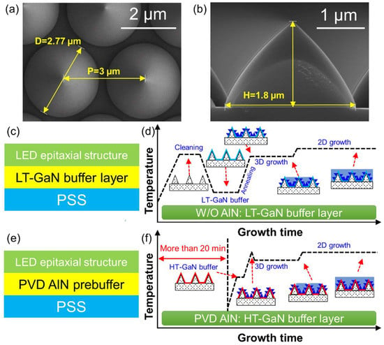
Figure 2.
(a) Plane-view and (b) cross-sectional SEM images of PSS; (c) schematic diagram and (d) schematic curve of temperature transients of LED epitaxial structure with LT-GaN buffer layer; (e) schematic diagram and (f) schematic curve of temperature transients of LED epitaxial structure with PVD AlN prebuffer layer.
The AlN prebuffer layer with a thickness of ~20 nm was deposited on PSS by PVD (Endura 300, Applied Materials, Inc., Santa Clara, CA, USA). Afterward, the AlN/PSS templates were loaded into the MOCVD reactor for the growth of LED epilayers. The corresponding schematic diagram of the epitaxial structure and trace-record curve of temperature transients were depicted in Figure 2e,f. An HT buffer layer was directly deposited on the template followed by the 3D island and 2D lateral deposition process after a heating ramp. In this case, the complicated heating and cooling ramp lasting of the LT buffer were simplified. This shortened the growth time by more than 20 min and increased the productivity by ~8%. Considering the high operating cost of MOCVD, the introduction of PVD AlN prebuffer layer in nitride epitaxy provides a new thought for the high-efficiency and low-cost growth of nitrides, which is meaningful in industrialized mass production.
Consequently, a trial-produced BLED film on a 4-inch PSS comparing the W/O AlN and PVD AlN prebuffer was executed to investigate the material quality and LED characteristics. The mean full width at half maximum (FWHM) values of the (0002) and (10–12) rocking curves were measured as 259, 252 arcsec for W/O AlN, and 130, 180 arcsec for PVD AlN prebuffer, respectively (see Figure 3a). Therefore, the screw threading dislocation density (TDD) and edge TDD are derived as: (a) 1.34 × 10⁸ and 3.16 × 108 cm−3 for W/O AlN, and (b) 3.4 × 10⁷ and 2.65 × 108 cm−3 for PVD AlN prebuffer [40], which indicates that the screw TDD drops by approximately an order of magnitude and the edge TDD decreases slightly. Cross-sectional TEM images of LED epilayers are shown in Figure 3b,c, which verifies that the TDD is effectively reduced for BLEDs with the PVD AlN prebuffer. Improvement of crystalline quality could benefit the ηint of the LED structure via suppressing the Shockley–Read–Hall recombination process. [41]. As discussed, an HT buffer layer was implemented on PVD AlN prebuffer layer. Therefore, different growth temperatures for HT buffer layer were executed in MOCVD. From Figure 3d, it can be observed that as the temperature increases, the color of the wafer gradually fades from dark yellow to nearly transparent, suggesting the reduction of defect densities under HT conditions. Therefore, the LT GaN buffer layer absorbs more blue light emitted from MQWs because of the defect-related photoluminescence when the LED device is operated. This is bad for enhancing ηext [42].
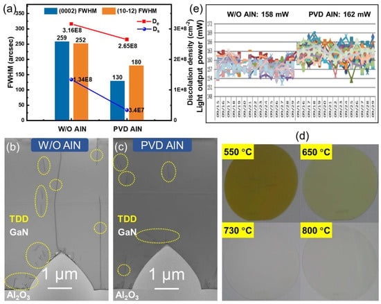
Figure 3.
(a) The mean FWHM values of (0002) and (10–12) rocking curves of epitaxial wafers utilizing W/O AlN and PVD AlN prebuffer, Ds: screw TDD, De: edge TDD; TEM images of BLED epilayers using (b) W/O AlN, (c) PVD AlN prebuffer; (d) The optical photo of the wafers, in which the GaN buffer layer was grown at 550, 650, 730, and 800 °C using PVD AlN prebuffer. (e) φe data logging results of mass production wafers using W/O AlN and PVD AlN prebuffer for half a month.
The average φe data of each batch of wafers in different reactors were recorded daily (see Figure 3e). The average φe of all wafers over half a month duration test for W/O AlN and PVD AlN prebuffer are around 158 and 162 mW, respectively. This suggests that the φe of BLED has been increased by 2.53%, in which accidental factors are excluded based on the statistics of the quantity. In summary, the development of PVD AlN prebuffer not only improves the production efficiency, but also optimizes the working performance of LED devices.
3.2. TPSS Technology
In this section, a novel TPSS technology was introduced in the BLED structure compared with conventional PSS technology mainly for the promotion of ηext through pilot study. For TPSS, the cone material is replaced from sapphire to silica, with a size of H = 2.1 µm, D = 2.9 µm, and periodicity of p = 3.1 µm, which is the same as the features of PSS (see Figure 4a,b). These two technologies combined with PVD AlN prebuffer were adopted to grow LED epitaxial structures, and the MQW layer was located approximately 100 nm from the top.
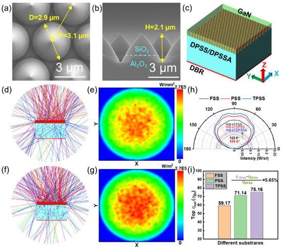
Figure 4.
(a) Plane-view and (b) cross-sectional SEM images of TPSS; (c) The simulated modeling of BLED-PSS or BLED-TPSS; (d) Cross-sectional ray-tracing and (e) radiation patterns on hemisphere surface of BLED-PSS; (f) Cross-sectional ray-tracing and (g) radiation patterns on hemisphere surface of BLED-TPSS; (h) Simulated far-field radiation patterns and (i) calculated top ηext of BLED-FSS, BLED-PSS, and BLED-TPSS.
To save computational memory, the BLED modeling was simplified as four layers, including an active region, GaN epilayer, substrates layer, and DBR layer with a reflectivity of 99% from top to bottom (see Figure 4c). The cross-sectional ray-tracing of BLED-FSS, BLED-PSS, BLED-TPSS, and corresponding radiation patterns on the hemisphere surface are sketched in Figure S1d–e and Figure 4d–g. It is observed that the BLED-PSS and BLED-TPSS exhibit significantly enhanced light emissions in all directions compared with the BLED-FSS. It is worth mentioning that BLED-TPSS demonstrates a stronger upward and weaker downward light distribution than BLED-PSS. The intensity mapping of the φe density in Figure 4g for BLED-TPSS is higher than that in Figure 4e for BLED-PSS. This is consistent with the results of ray-tracing. Figure 4h presents the simulated far-field radiation patterns of BLEDs on different substrates. We assume that the pattern is an ideal symmetrical distribution and the result in the range of 0–90° is simulated. For the emission intensity, that of BLED-TPSS is the highest at almost all launch angles. In terms of the half-value (HV) angle, BLED-FSS, BLED-PSS, and BLED-TPSS are 122.6°, 123.4°, and 123.4°, respectively. This means that BLED-PSS and BLED-TPSS have almost the same emission HV angle, which is slightly wider than BLED-FSS. The top ηext values of the three-type LEDs are 59.17%, 71.14%, and 75.16%, as shown in Figure 4i. Compared with BLED-PSS, the top ηext of BLED-TPSS is increased by 5.65%. Although a small value appears, it is a large breakthrough for industrial production. As the reflectivity of the epitaxial structure is an important factor for LED light extraction, the reflectivity of BLED-PSS and BLED-TPSS wafers was measured to investigate the collimated ηext effect (see Figure 5a,b). The reflectivity of BLED-TPSS is slightly higher than that of BLED-PSS in the range of incident light wavelengths from ultraviolet to near-infrared. In particular, a significant improvement of 4.06% at 450 nm is observed, explaining the stronger ηext intensity along the axial direction, which coincides with the simulated results. In addition, during the epitaxial process, AlN/TPSS could improve the interfacial growth front compared to AlN/PSS (see Figure S2), with detailed discussion in Supplementary Materials. The thickness of epitaxial LED structure on both AlN/PSS and AlN/TPSS is around 5.75 µm (see Figure S3).
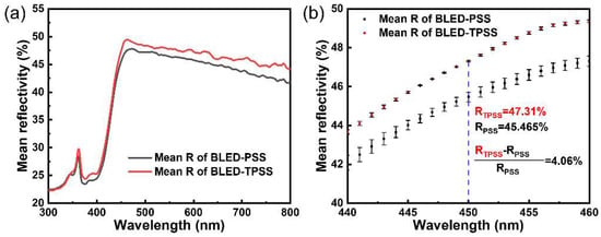
Figure 5.
(a) Reflection spectra of BLED-PSS and BLED-TPSS wafers with incident wavelengths from 300 nm to 800 nm; (b) Zoomed reflection spectra at incident wavelengths around 450 nm.
3.3. High Light Output Power BLED
The BLED devices were fabricated with dimensions of 22 × 40 mil2, using PSS and TPSS combined with PVD-AlN prebuffer. φe of BLED-TPSS (φe-TPSS) and φe of BLED-PSS (φe-PSS) versus Jin are sketched in Figure 6a. The relative enhancement of φe (φe-relative) is described as the ratio of difference φe (φe-diff) to φe-DPSS, expressed as φe-diff/φe-PSS (see Figure 6b). It can be seen that φe-TPSS is slightly lower than φe-PSS when Jin is less than 0.16 A/cm2. However, φe-TPSS is higher in a large current density range greater than 0.16 A/cm2. As Jin increases, φe-relative shows logarithmic growth first when Jin is less than 6.8 A/cm2, and then exhibits a linear increase when Jin is greater than 6.8 A/cm2. The φe-relative has exceeded 10% at a Jin of 40 A/cm2.
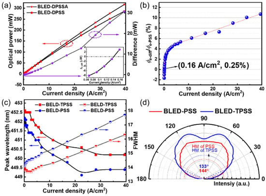
Figure 6.
(a) φe and its difference, (b) the φe enhancement, (c) λp and FWHM of BLED-PSS and BLED-TPSS chips as functions of Jin, the inset of (a) is an expansion of φe-diff in the range of Jin less than 0.16 A/cm2; (d) Experimentally measured far-field radiation patterns of BLED-PSS and BLED-TPSS.
The peak wavelength (λp) and FWHM of the electroluminescence (EL) spectra are presented in Figure 6c. The λp of both BLED-PSS and BLED-TPSS is located at approximately 450 nm, corresponding to the radiation recombination of electron–hole pairs of blue emission. λp blueshifts from 452.2 to 449.4 nm for BLED-PSS, and 452.6 to 450.2 nm for BLED-TPSS as Jin increases from 0.07 to 39.5 A/cm2. In this case, a quantum-confined Stark effect (QCSE) is generated within the MQW region at no Jin caused by spontaneous and built-in piezoelectric fields, especially for the LED structure [43], which will reduce the overlap integral of electron/hole wave-functions. As a result, the charge screening and band filling effects would gradually weaken the QCSE as Jin increases, subsequently leading to a blueshift in the λp. The FWHM of both LEDs behaves faintly larger when Jin changes from 0.07 to 40 A/cm2. This is ascribed to the native fluctuation of In composition in MQWs, and more electron–hole pairs would be excited as Jin increases [44]. Far-field radiation patterns of BLED-PSS and BLED-TPSS in the range of 0–90° are experimentally measured (see Figure 6d). Compared to BLED-PSS, BLED-TPSS exhibits a higher relative intensity, which is consistent with the simulation results. However, the deviation is that the HVs of BLED-PSS and BLED-TPSS are larger than the simulated results, in which the experimental results are affected by many processes, such as dicing, gold wires, and package substrate. Additionally, BLED-TPSS has a more convergent emission pattern with an HV 11° lower than that of BLED-PSS.
3.4. High Luminous Efficacy WLED
We fabricated WBEDs by incorporating BLEDs and yellow phosphor through a PC-LED package strategy. The Jin dependence of ηL, wall-plug efficiency (WPE), operated voltage, and φe are shown in Figure 7. The peak ηL and peak WPE reach maxima of 295.2 lm/W and 63.2%, respectively, at a Jin of 0.9 A/cm2. It is worth noting that the ηL and WPE retained 282.4 lm/W and 60.4% at a Jin of 5.6 A/cm2, respectively. The ηL and WPE decrease as Jin (greater than 0.9 A/cm2) increases, which is the common droop effect for LED devices. It may originate from Auger recombination, carrier leakage, carrier localization, and other factors [45,46].
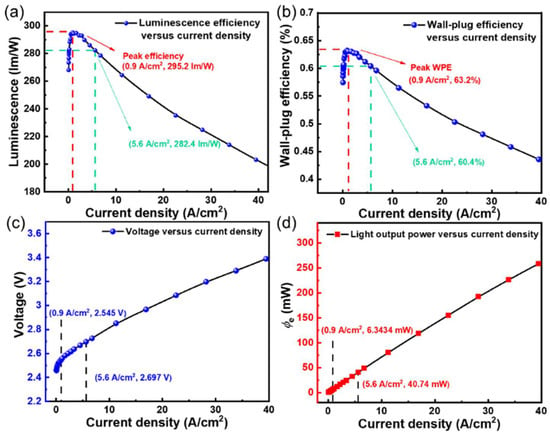
Figure 7.
(a) ηL as a function of Jin for WLEDs; (b) WPE as functions of Jin for white LEDs; (c) Jin and (d) φe dependence of operating voltage for WLEDs.
The J-V curve of the WLED demonstrates good rectification characteristics with two representative points of (0.9 A/cm2, 2.55 V), (5.6 A/cm2, 2.7 V). The φe shows a linear increase with increasing Jin and reaches 40.74 mW at a Jin of 5.6 A/cm2. The correlated color temperature (CCT) was measured as 4592 K, where neutral white light was obtained. This work has significantly enhanced the brightness of WLEDs, which is expected to promote the applications of superior solid-state lighting in general lighting, high-power lighting, and display fields in the future.
4. Conclusions
In summary, high-efficiency WLEDs have been demonstrated by adopting PVD AlN prebuffer and TPSS technology. The ηL reaches 295.2 lm/W and 282.4 lm/W at Jin of 0.9 A/cm2 and 5.6 A/cm2, respectively. The PVD AlN prebuffer enables the screw TDD to drop by approximately an order of magnitude from 1.34 × 10⁸ to 3.4 × 107 cm−3. It then enhances the φe of BLEDs by 2.53% via batch data statistics, while increasing the productivity of ~8%. Monte Carlo ray-tracing simulations show that the top ηext has been increased from 71.14% for BLED-PSS to 75.16% for BLED-TPSS. The reflectivity of light peaking at 450 nm for BLED-TPSS is enhanced by 4.06%, and the φe is promoted by 10% at a Jin of 40 A/cm2. The goal of this work is to reduce energy waste with technological innovations in solid-state lighting to achieve higher quantum efficiency. Future work will focus on the mature mass production and commercialization of the strategies proposed in this work.
Supplementary Materials
The following supporting information can be downloaded at: https://www.mdpi.com/article/10.3390/nano12101638/s1, Figure S1. Ray-tracing results of BLED on (a) FSS, (b) PSS, (c) TPSS using hemispherical perfect absorber model; (d) Cross-sectional ray-tracing and, (e) radiation patterns on hemisphere surface of BLED on FSS. Figure S2. (a) Cross-section and (b) plane-view SEM images of GaN 3D growth on AlN/PSS template; (c) Cross-section and (d) plane-view SEM images of GaN 3D growth on AlN/TPSS template. Figure S3. Cross-section SEM images of LED epitaxial structure on (a) AlN/PSS template and (b) AlN/TPSS template.
Author Contributions
S.Z. and M.L. contributed equally to this work. Design and execution of experiments, S.Z. and M.L.; formal analysis, S.Z. and M.L.; supervision and discussion of results, Y.Y., J.H., Y.L., T.F., X.Z., Z.L. (Zhicong Li) and C.X.; validation, S.Z. and M.L.; writing—original draft preparation, S.Z. and M.L.; writing—review and editing, S.Z., M.L., J.W., J.L., Z.L. (Zhiqiang Liu) and X.Y.; project administration, J.W., J.L., Z.L. (Zhiqiang Liu) and X.Y.; funding acquisition, Z.L. (Zhiqiang Liu) and X.Y. All authors have read and agreed to the published version of the manuscript.
Funding
This research was funded by the National Key R&D Program of China (Grant Nos. 2017YFB0403100 and 2017YFB0403103), and the National Natural Science Foundation of China (Grant Nos. 62174157 and 61974140).
Institutional Review Board Statement
Not applicable.
Informed Consent Statement
Not applicable.
Data Availability Statement
The data presented in this study are available on request from the corresponding author.
Conflicts of Interest
The authors declare no conflict of interest.
References
- Nakamura, S. Current Status of GaN-Based SolidState Lighting. MRS Bull. 2009, 34, 101–107. [Google Scholar] [CrossRef]
- Zhang, Y.; Xie, H.; Zheng, H.; Wei, T.; Yang, H.; Li, J.; Yi, X.; Song, X.; Wang, G.; Li, J. Light extraction efficiency improvement by multiple laser stealth dicing in InGaN-based blue light-emitting diodes. Opt. Express 2012, 20, 6808–6815. [Google Scholar] [CrossRef] [PubMed]
- Wu, H.; Li, H.; Kuo, S.-Y.; Chen, B.-Y.; Lu, T.-C.; Huang, H. High Output Power GaN-Based Green Resonant-Cavity Light-Emitting Diodes with Trapezoidal Quantum Wells. IEEE Trans. Electron Devices 2020, 67, 3650–3654. [Google Scholar] [CrossRef]
- Ponce, F.A.; Bour, D.P. Nitride-based semiconductors for blue and green light-emitting devices. Nature 1997, 386, 351–359. [Google Scholar] [CrossRef]
- Wu, T.; Sher, C.-W.; Lin, Y.; Lee, C.-F.; Liang, S.; Lu, Y.; Chen, S.-W.H.; Guo, W.; Kuo, H.-C.; Chen, Z. Mini-LED and Micro-LED: Promising Candidates for the Next Generation Display Technology. Appl. Sci. 2018, 8, 1557. [Google Scholar] [CrossRef] [Green Version]
- Zhang, S.; Yan, Y.; Feng, T.; Yin, Y.; Ren, F.; Liang, M.; Wu, C.; Yi, X.; Wang, J.; Li, J.; et al. Wafer-Scale Semipolar Micro-Pyramid Lighting-Emitting Diode Array. Crystals 2021, 11, 686. [Google Scholar] [CrossRef]
- Huang, Y.; Guo, Z.; Wang, X.; Li, H.; Xiang, D. GaN-Based High-Response Frequency and High-Optical Power Matrix Micro-LED for Visible Light Communication. IEEE Electron Device Lett. 2020, 41, 1536–1539. [Google Scholar] [CrossRef]
- Singh, K.J.; Huang, Y.-M.; Ahmed, T.; Liu, A.-C.; Chen, S.-W.H.; Liou, F.-J.; Wu, T.; Lin, C.-C.; Chow, C.-W.; Lin, G.-R.; et al. Micro-LED as a Promising Candidate for High-Speed Visible Light Communication. Appl. Sci. 2020, 10, 7384. [Google Scholar] [CrossRef]
- Li, M.; Zhang, X.; Zhang, H.; Chen, W.; Ma, L.; Wang, X.; Liu, Y.; Lei, B. Highly efficient and dual broad emitting light convertor: An option for next-generation plant growth LEDs. J. Mater. Chem. C 2019, 7, 3617–3622. [Google Scholar] [CrossRef]
- Lin, C.; Zhan, T.; Liu, Z.; Yi, X.; Xie, H.; Wang, J.; Li, J. A Wirelessly Controllable Optoelectronic Device for Optogenetics. IEEE. Photon-Technol. Lett. 2019, 31, 915–918. [Google Scholar] [CrossRef]
- Cheng, I.-H.; McBride, J.; Decker, M.; Watson, T.; Jakubenko, H.; Russo, A. The asylum seeker integrated healthcare pathway: A collaborative approach to improving access to primary health care in South Eastern Melbourne, Victoria, Australia. Aust. J. Prim. Health 2019, 25, 6–12. [Google Scholar] [CrossRef] [PubMed]
- Pimputkar, S.; Speck, J.S.; Steven, P.D.; Nakamura, S. Prospects for LED lighting. Nat. Photonics 2009, 3, 180–182. [Google Scholar] [CrossRef]
- Chen, Z.; Zhang, X.; Dou, Z.; Wei, T.; Liu, Z.; Qi, Y.; Ci, H.; Wang, Y.; Li, Y.; Chang, H.; et al. High-Brightness Blue Light-Emitting Diodes Enabled by a Directly Grown Graphene Buffer Layer. Adv. Mater. 2018, 30, e1801608. [Google Scholar] [CrossRef] [PubMed]
- Liu, Y.; Silver, J.; Xie, R.-J.; Zhang, J.; Xu, H.; Shao, H.; Jiang, J.; Jiang, H. An excellent cyan-emitting orthosilicate phosphor for NUV-pumped white LED application. J. Mater. Chem. C 2017, 5, 12365–12377. [Google Scholar] [CrossRef]
- Khan, W.U.; Zhou, L.; Li, X.; Zhou, W.; Khan, D.; Niaz, S.-I.; Wu, M. Single phase white LED phosphor Ca3YAl3B4O15:Ce3+,Tb3+,Sm3+ with superior performance: Color-tunable and energy transfer study. Chem. Eng. J. 2021, 410, 128455. [Google Scholar] [CrossRef]
- Chandra, F.; Wahyudianto, A.; Yasin, M. Design of vein finder with multi tuning wavelength using RGB LED. J. Phys. Conf. Ser. 2017, 853, 012019. [Google Scholar] [CrossRef]
- TEHNOBLOG. SMD LED Chips Characteristics: Size, Power, Efficacy. Available online: https://tehnoblog.org/smd-led-chips-characteristics-size-power-efficiency/ (accessed on 24 August 2021).
- United States Department of Energy. 2019 Lighting R&D Opportunities; United States Department of Energy: Washington, DC, USA, 2020.
- Cree, I. Cree First to Break 300 Lumens-Per-Watt Barrier. Available online: https://www.wolfspeed.com/company/news-events/news/cree-first-to-break-300-lumens-per-watt-barrier (accessed on 26 March 2014).
- Amano, H.; Sawaki, N.; Akasaki, I.; Toyoda, Y. Metalorganic vapor phase epitaxial growth of a high quality GaN film using an AlN buffer layer. Appl. Phys. Lett. 1986, 48, 353–355. [Google Scholar] [CrossRef] [Green Version]
- He, C.; Zhao, W.; Zhang, K.; He, L.; Wu, H.; Liu, N.; Zhang, S.; Liu, X.; Chen, Z. High-Quality GaN Epilayers Achieved by Facet-Controlled Epitaxial Lateral Overgrowth on Sputtered AlN/PSS Templates. ACS Appl. Mater. Interfaces 2017, 9, 43386–43392. [Google Scholar] [CrossRef]
- Lee, D.; Lee, S.; Kim, G.; Kim, J.; Jang, J.; Oh, J.; Moon, D.; Park, Y.; Yoon, E. Epitaxial lateral overgrowth of GaN on nano-cavity patterned sapphire substrates. J. Cryst. Growth 2019, 507, 103–108. [Google Scholar] [CrossRef]
- Chao, S.-H.; Yeh, L.-H.; Wu, R.T.; Kawagishi, K.; Hsu, S.-C. Novel patterned sapphire substrates for enhancing the efficiency of GaN-based light-emitting diodes. RSC Adv. 2020, 10, 16284–16290. [Google Scholar] [CrossRef] [Green Version]
- Cho, J.-Y.; Kim, J.-S.; Kim, Y.-D.; Cha, H.J.; Lee, H. Fabrication of oxide-based nano-patterned sapphire substrate to improve the efficiency of GaN-based of LED. Jpn. J. Appl. Phys. 2015, 54, 02BA04. [Google Scholar] [CrossRef]
- Prajoon, P.; Menokey, M.A.; Pravin, J.C.; Ajayan, J.; Rajesh, S.; Nirmal, D. Investigation of efficiency enhancement in InGaN MQW LED with compositionally step graded GaN/InAlN/GaN multi-layer barrier. Superlattice Microstruct. 2018, 116, 71–78. [Google Scholar] [CrossRef]
- Karan, H.; Biswas, A. Improving performance of light-emitting diodes using InGaN/GaN MQWs with varying trapezoidal bottom well width. Optik 2021, 247, 167888. [Google Scholar] [CrossRef]
- Usman, M.; Munsif, M.; Anwar, A.-R. Wedge-shaped electron blocking layer to improve hole transport and efficiency in green light-emitting diodes. Opt. Commun. 2020, 464, 125493. [Google Scholar] [CrossRef]
- Wang, T.-H.; Xu, J.-L. Advantage of InGaN-based light-emitting diodes with trapezoidal electron blocking layer. Mater. Sci. Semicond. Process. 2015, 29, 95–101. [Google Scholar] [CrossRef]
- Liu, Z.; Yi, X.; Yu, Z.; Yuan, G.; Liu, Y.; Wang, J.; Li, J.; Lu, N.; Ferguson, I.; Zhang, Y. Impurity Resonant States p-type Doping in Wide-Band-Gap Nitrides. Sci. Rep. 2016, 6, 19537. [Google Scholar] [CrossRef]
- Moon, Y.-J.; Moon, D.-Y.; Jang, J.; Na, J.-Y.; Song, J.-H.; Seo, M.-K.; Kim, S.; Bae, D.; Park, E.H.; Park, Y.; et al. Microstructured Air Cavities as High-Index Contrast Substrates with Strong Diffraction for Light-Emitting Diodes. Nano Lett. 2016, 16, 3301–3308. [Google Scholar] [CrossRef]
- Zhou, S.; Liu, X.; Yan, H.; Chen, Z.; Liu, Y.; Liu, S. Highly efficient GaN-based high-power flip-chip light-emitting diodes. Opt. Express 2019, 27, A669–A692. [Google Scholar] [CrossRef]
- Lee, G.S.; Lee, C.; Jeon, H.; Lee, C.; Bae, S.G.; Ahn, H.S.; Yang, M.; Yi, S.N.; Yu, Y.M.; Lee, J.H.; et al. Growth of AlN layer on patterned sapphire substrate by hydride vapor phase epitaxy. Jpn. J. Appl. Phys. 2016, 55, 05FC02. [Google Scholar] [CrossRef]
- Zhu, H.; Lin, C.C.; Luo, W.; Shu, S.; Liu, Z.; Liu, Y.; Kong, J.; Ma, E.; Cao, Y.; Liu, R.-S.; et al. Highly efficient non-rare-earth red emitting phosphor for warm white light-emitting diodes. Nat. Commun. 2014, 5, 4312. [Google Scholar] [CrossRef] [Green Version]
- Pust, P.; Weiler, V.; Hecht, C.; Tücks, A.; Wochnik, A.S.; Henß, A.-K.; Wiechert, D.; Scheu, C.; Schmidt, P.J.; Schnick, W. Narrow-band red-emitting Sr[LiAl3N4]:Eu2+ as a next-generation LED-phosphor material. Nat. Mater. 2014, 13, 891–896. [Google Scholar] [CrossRef] [PubMed]
- Yang, X.; Zhang, J.; Wang, X.; Zheng, C.; Quan, Z.; Jiang, F. Enhance the efficiency of green-yellow LED by optimizing the growth condition of preparation layer. Superlattices Microstruct. 2020, 141, 106459. [Google Scholar] [CrossRef]
- Park, J.H.; Kim, D.Y.; Hwang, S.; Meyaard, D.; Schubert, E.F.; Han, Y.D.; Choi, J.W.; Cho, J.; Kim, J.K. Enhanced overall efficiency of GaInN-based light-emitting diodes with reduced efficiency droop by Al-composition-graded AlGaN/GaN superlattice electron blocking layer. Appl. Phys. Lett. 2013, 103, 061104. [Google Scholar] [CrossRef] [Green Version]
- Li, L.; Stegmann, P.G.; Rosenkranz, S.; Schäfer, W.; Tropea, C. Simulation of light scattering from a colloidal droplet using a polarized Monte Carlo method: Application to the time-shift technique. Opt. Express 2019, 27, 36388–36404. [Google Scholar] [CrossRef]
- Zhang, S.; Liu, B.; Ren, F.; Yin, Y.; Wang, Y.; Chen, Z.; Jiang, B.; Liu, B.; Liu, Z.; Sun, J.; et al. Graphene-Nanorod Enhanced Quasi-Van Der Waals Epitaxy for High Indium Composition Nitride Films. Small 2021, 17, e2100098. [Google Scholar] [CrossRef]
- Nakamura, S. GaN Growth Using GaN Buffer Layer. Jpn. J. Appl. Phys. 1991, 30, L1705–L1707. [Google Scholar] [CrossRef]
- Ni, R.; Chen, X.; Yan, J.; Zhang, L.; Guo, Y.; Wang, J.; Li, J.; Zhang, Y. Reducing stimulated emission threshold power density of AlGaN/AlN multiple quantum wells by nano-trench-patterned AlN template. J. Alloys Compd. 2019, 777, 344–349. [Google Scholar] [CrossRef]
- Chiu, C.-H.; Lin, D.-W.; Li, Z.-Y.; Chiu, C.-H.; Chao, C.-L.; Tu, C.-C.; Kuo, H.-C.; Lu, T.-C.; Wang, S.-C. Improvement in Crystalline Quality of InGaN-Based Epilayer on Sapphire via Nanoscaled Epitaxial Lateral Overgrowth. Jpn. J. Appl. Phys. 2010, 49, 105501. [Google Scholar] [CrossRef]
- Kaufmann, U.; Kunzer, M.; Obloh, H.; Maier, M.; Manz, C.; Ramakrishnan, A.; Santic, B. Origin of defect-related photoluminescence bands in doped and nominally undoped GaN. Phys. Rev. B 1999, 59, 5561–5567. [Google Scholar] [CrossRef]
- Wu, F.-L.; Ou, S.-L.; Kao, Y.-C.; Chen, C.-L.; Tseng, M.-C.; Lu, F.-C.; Lin, M.-T.; Horng, R.-H. Thin-film vertical-type AlGaInP LEDs fabricated by epitaxial lift-off process via the patterned design of Cu substrate. Opt. Express 2015, 23, 18156–18165. [Google Scholar] [CrossRef]
- Bi, Z.; Gustafsson, A.; Lenrick, F.; Lindgren, D.; Hultin, O.; Wallenberg, L.R.; Ohlsson, B.J.; Monemar, B.; Samuelson, L. High In-content InGaN nano-pyramids: Tuning crystal homogeneity by optimized nucleation of GaN seeds. J. Appl. Phys. 2018, 123, 025102. [Google Scholar] [CrossRef]
- Kioupakis, E.; Yan, Q.; Van de Walle, C.G. Interplay of polarization fields and Auger recombination in the efficiency droop of nitride light-emitting diodes. Appl. Phys. Lett. 2012, 101, 231107. [Google Scholar] [CrossRef] [Green Version]
- Li, H.; Li, P.; Kang, J.; Li, Z.; Zhang, Y.; Liang, M.; Li, Z.; Li, J.; Yi, X.; Wang, G. Analysis Model for Efficiency Droop of InGaN Light-Emitting Diodes Based on Reduced Effective Volume of Active Region by Carrier Localization. Appl. Phys. Express 2013, 6, 092101. [Google Scholar] [CrossRef]
Publisher’s Note: MDPI stays neutral with regard to jurisdictional claims in published maps and institutional affiliations. |
© 2022 by the authors. Licensee MDPI, Basel, Switzerland. This article is an open access article distributed under the terms and conditions of the Creative Commons Attribution (CC BY) license (https://creativecommons.org/licenses/by/4.0/).