Abstract
A dual broadband terahertz bifunction absorber that can be actively tuned is proposed. The optical properties of the absorber were simulated and numerically calculated using the finite-difference time-domain (FDTD) method. The results show that when the conductivity of vanadium dioxide is less than S/m, the absorptance can be continuously adjusted between 2% and 100%. At vanadium dioxide conductivity greater than S/m, the absorption bandwidth of the absorber can be switched from 3.4 THz and 3.06 THz to 2.83 THz and none, respectively, and the absorptance remains above 90%. This achieves perfect modulation of the absorptance and absorption bandwidth. The physical mechanism of dual-broadband absorptions and perfect absorption is elucidated by impedance matching theory and electric field distribution. In addition, it also has the advantage of being polarization insensitive and maintaining stable absorption at wide angles of oblique incidence. The absorber may have applications in emerging fields such as modulators, stealth and light-guided optical switches.
1. Introduction
In recent years, terahertz (THz) waves have attracted a great deal of attention because of their promising applications in wireless communications [1], sensors [2] and imaging [3]. As research into terahertz technology has advanced, various functional metamaterial devices have been proposed and theoretically investigated, such as fiber optic filters [4,5], absorbers [6,7,8,9,10], polarization converters [11] and hyperbolic metamaterials [12]. Among them, metamaterial perfect absorbers (MPAs) are widely used in the THz range due to their widespread applications in imaging [13,14], stealth technologies [15,16] and so on [17,18,19] and play a very important role within. In 2008, Landy et al. used a classical three-layer structure as a metamaterial perfect absorber (MPA) so that the incident wave was perfectly absorbed by the metamaterial absorber [20], and since then, various single-band [21,22,23,24], double-band [25,26,27,28] and multi-band absorbers [29,30] have been proposed. However, the absorption bandwidth of these MPAs are relatively narrow, and their electromagnetic responses cannot be adjusted after the structure has been determined, which limits their practical application. In order to achieve active tuning of the absorber in the terahertz band, we use the phase transition material vanadium dioxide (VO2) as the material for tuning the absorption. Many studies in recent years have shown that VO2 has significant optical change properties in the terahertz band and that the phase transition of VO2 from the insulator to the metal phase is around 340 K. It can be triggered by electrical [31,32,33], thermal [34,35] or optical excitation [36,37], with changes of several orders of magnitude in electrical conductivity during this time. Additionally, the phase transition from insulator to metal is accompanied by a steady increase in the conductivity of VO2. Therefore, utilizing vanadium dioxide as an absorber material is an effective way to realize the active tuning of absorbers [38,39,40,41].
In this work, a tunable dual-broadband terahertz absorber based on VO2 metamaterial is proposed. It consists of four vanadium dioxide fillet cavities, a TOPAS dielectric spacer layer, vanadium dioxide film, a silica dielectric layer and gold film from top to bottom. All materials are homogeneous [42]. The theoretical study of the absorber uses FDTD and impedance matching theory. The simulation results show that the efficiency and bandwidth of absorption can be changed by tuning the conductivity of vanadium dioxide. Moreover, the absorber is insensitive to the polarization of incident light and is able to maintain absorption stability at large angles of oblique incidence. The absorber provides a new scheme for tunable dual-broadband absorbers with broad application prospects in modulators, stealth and photoconductive light switches.
2. Materials and Methods
Design and Simulation
As shown in Figure 1a,b, the schematic diagram of the designed metamaterial absorber, each cell is composed of four vanadium dioxide fillet cavities, a TOPAS dielectric spacer, a vanadium dioxide film, a silicon dioxide (SiO2) layer and gold film from top to bottom. The thicknesses of the vanadium dioxide fillet cavities, the TOPAS, vanadium dioxide thin-films, the silicon dioxide layer and the gold are t1 = 0.3 µm, t2 = 14 µm, t3 = 0.81 µm, t4 = 10 µm and t5 = 0.4 µm, respectively. Figure 1c is a top view of the unit, and the geometric parameters of the vanadium dioxide fillet cavity are L = 21 µm, d = 19 µm, w = 5.5 µm. The composite dielectric constant of the TOPAS is . TOPAS is a transparent, easy to produce thermoplastic copolymer with constant refractive index and negligible absorption coefficient in the terahertz range, which is widely used in terahertz devices. The conductivity of gold and the relative permittivity of SiO2 are S/m and , respectively. The performance of the designed absorber is theoretically studied by using the FDTD method (Lumerical Solutions, Vancouver, BC, Canada). In the simulations, the boundary conditions in the x and y directions are set as periodic boundaries and the boundary conditions in the z direction are set as perfectly matched layers. The absorption can be defined as , where is the reflectance. As the thickness of the gold film is greater than the penetration depth of the THz wave, transmittance is . The optical permittivity of VO2 in the THz range can be described by the Drude model [43,44]:
where is the permittivity at the infinite frequency, rad/s is the collision frequency and the plasma frequency at can be given by with S/m and S/m. In this paper, the conductivity of vanadium dioxide in the insulator phase and the metal phase are assumed to be S/m and S/m, respectively.
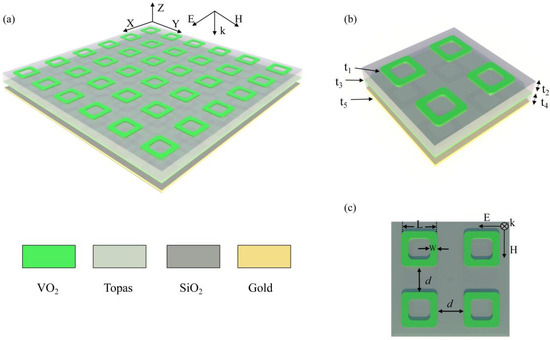
Figure 1.
(a) Schematic diagram of the whole proposed 3D structure. (b) Schematic of a unit cell. (c) Top view of a unit cell.
3. Results
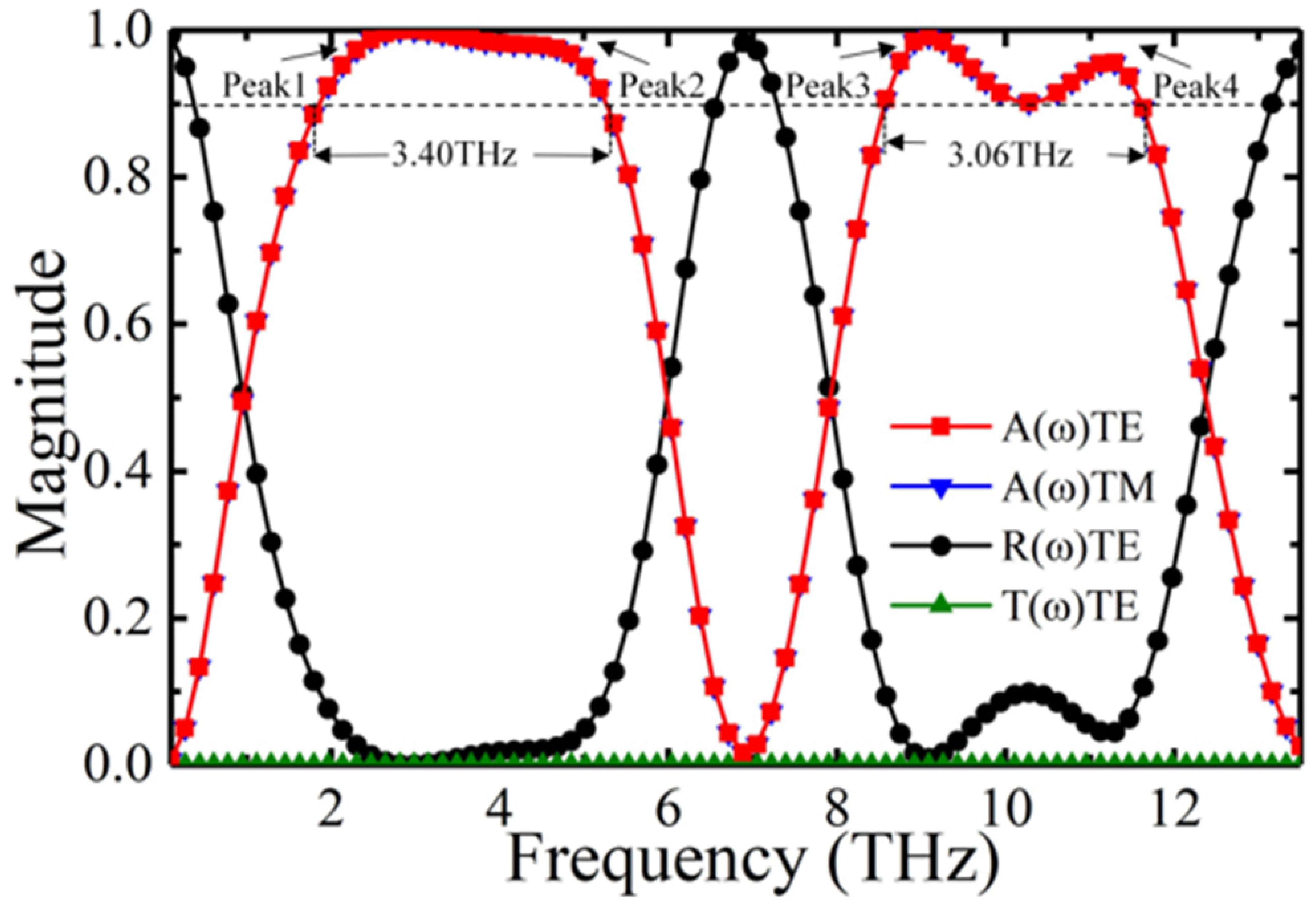
Figure 2 shows the absorption, reflection and transmission spectra of the absorber at the vanadium dioxide conductivity S/m. Due to the symmetry of the structure, the linear and elliptic angle polarization have no effect on absorption. In the linear angle polarization, the absorptance for the transverse electric (TE) and transverse magnetic (TM) polarizations are consistent. It follows that the absorber is polarization insensitive. The absorber exhibits outstanding absorptance and absorption bandwidth as the terahertz waves are confined to the surface by the vanadium dioxide, producing a localized surface plasma resonance. The absorption bandwidth of 90% absorptance under normal incidence is between 1.85 and 5.25 THz and 8.56 and 11.6 THz, up to 3.4 THz and 3.06 THz, respectively. There are four perfect absorption peaks, with Peak 1 = 2.95 THz, Peak 2 = 4.4 THz, Peak 3 = 9.1 THz and Peak 4 = 11.3 THz. Since there is a sufficiently thick gold film at the bottom of the absorber, the transmittance is 0.

Figure 2.
Absorption, reflection and transmission spectra.
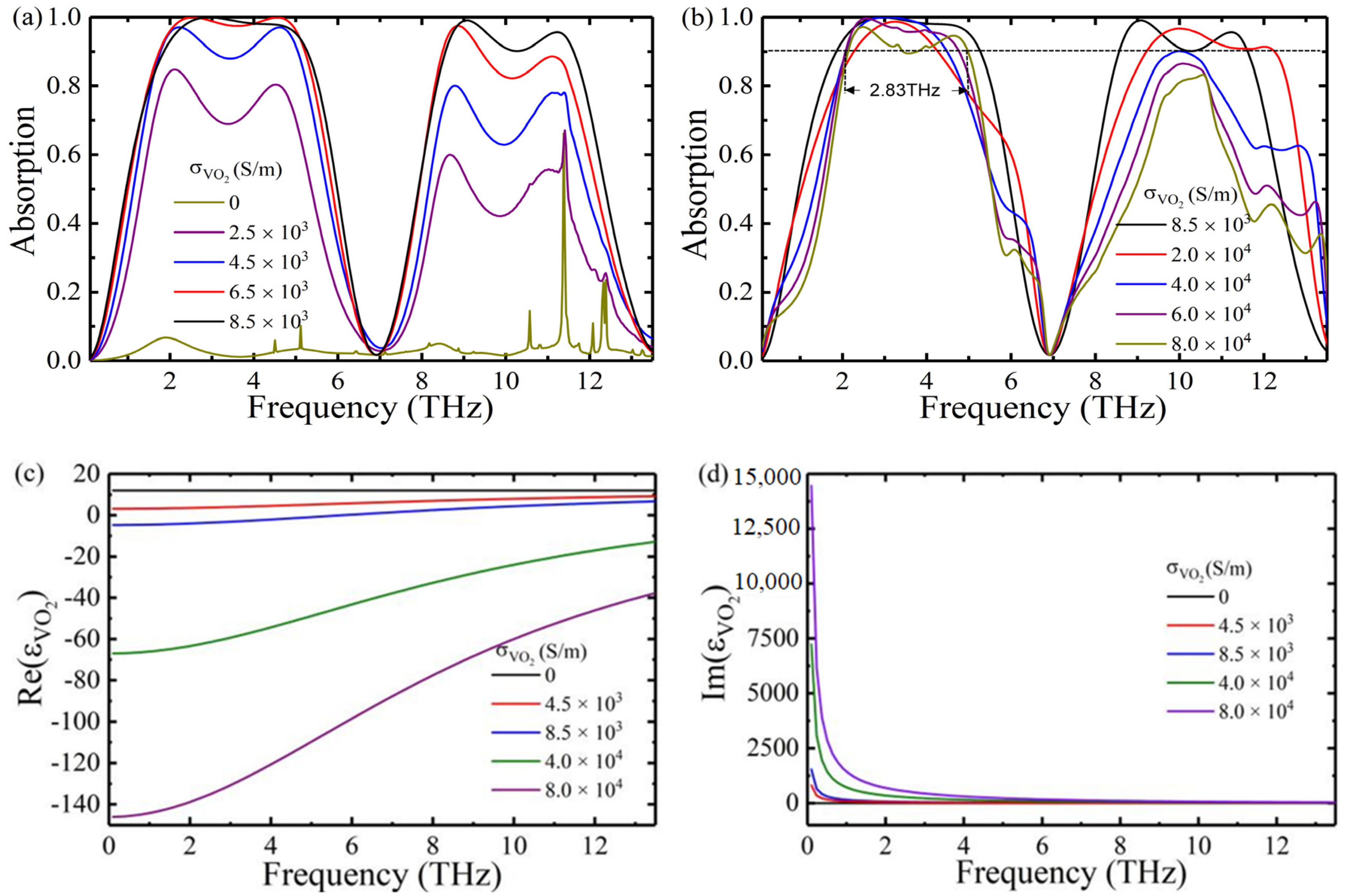
We calculated the reflectance and transmittance of the absorber at different vanadium dioxide conductivities using the s-parameters. According to the formula for the absorption, , we can obtain the absorption spectrum of the absorber for different vanadium dioxide conductivities. The absorption spectrum of the conductivity of vanadium dioxide varying from S/m to S/m is shown in Figure 3a. As the conductivity increases, the absorptance can be dynamically adjusted from 2% to 100%. The main reason for this phenomenon is that it undergoes an optical transition from dielectric to metal when the conductivity increases from S/m to S/m. The greater the conductivity, the better the metal behavior and the higher the absorptance. As shown in Figure 3b, when the conductivity increases from S/m to S/m, the absorption bandwidth can be switched from 3.4 THz and 3.06 THz to 2.83 THz and none, respectively. The metal behavior of vanadium dioxide increases as its conductivity increases. Only the upper three-layer structure achieves absorption performance, and the lower layer structure does not work, so the absorption bandwidth decreases. The real and imaginary parts of the relative permittivity of the VO2 for different conductivities are shown in Figure 3c,d. The results show that the variation in the imaginary part is much greater than the variation in the real part for the different conductivities. This results in a significant variation in the absorptance and absorption bandwidth [25,43,44].
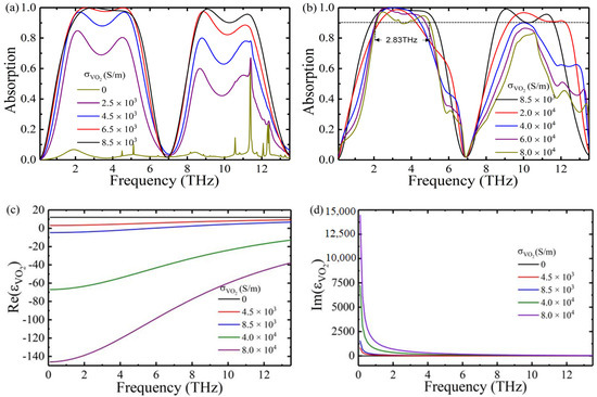
Figure 3.
(a) Absorption spectrum of VO2 increasing from S/m to S/m and (b) S/m to S/m. (c) Real parts and (d) imaginary parts of permittivity with different conductivities of VO2.
The absorption mechanism of this dual-broadband absorber can be well explained by impedance matching theory. When the effective impedance of the absorber matches the effective impedance of the free space, the reflectance is minimized, and the absorptance and relative impedance can be obtained as follows:
where and are the effective impedance of the free space and the absorber, is the relative impedance and and represent the reflectance and transmittance of the absorber, respectively. The gold film on the bottom of the absorber makes terahertz waves impenetrable, so is zero. Figure 4a,b shows the real and imaginary parts of the relative impedance of vanadium dioxide at different conductivities. The results show that when the conductivity of VO2 is S/m, the real part gradually reaches 1 and the imaginary part gradually reaches 0 in the frequency ranges of 1.85–5.25 THz and 8.54–11.6 THz, respectively. It follows that the impedances of the absorber and free space gradually match, which can absorb the incident wave to the maximum extent.
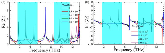
Figure 4.
(a) Real parts and (b) imaginary parts of the relative impedance with different conductivities of VO2.
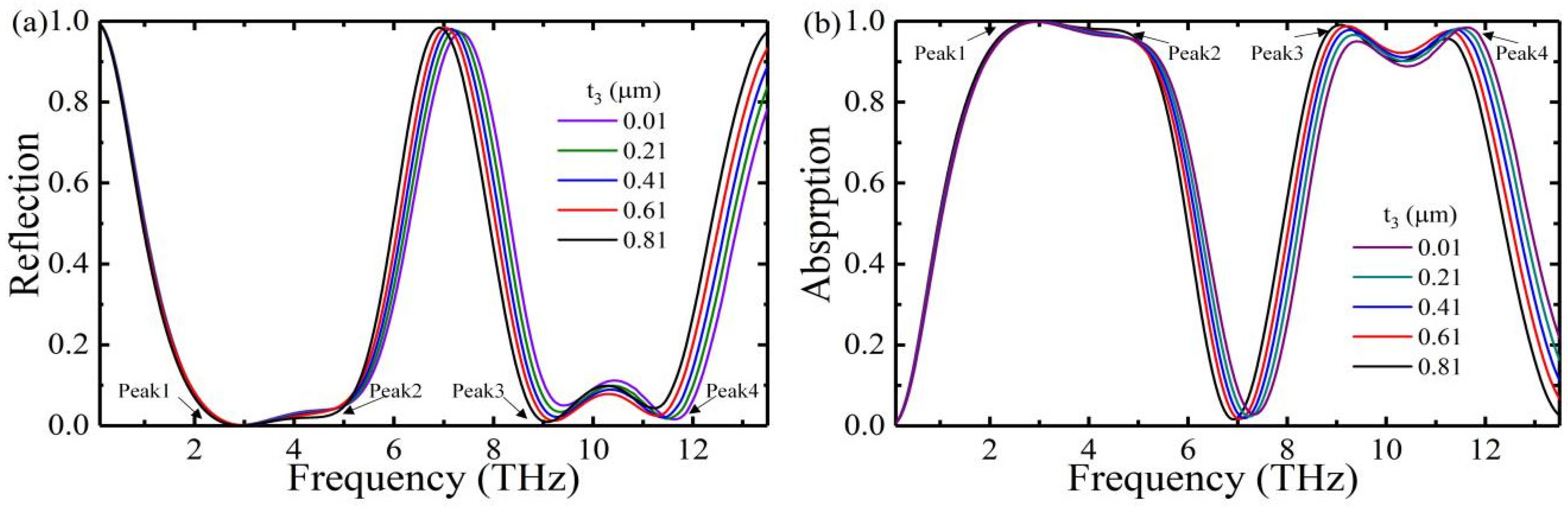
Furthermore, we also investigated the relationship between the reflectance and absorptance of this absorber and the thickness of the vanadium dioxide film. Figure 5a,b shows the reflectance and absorptance of vanadium dioxide at a fixed conductivity of S/m. The results show that when the thickness of the vanadium dioxide film increases from 0.01 µm to 0.81 µm, the two broad absorption bands are red-shifted. As shown in Figure 5a, the reflectance of Peak 1 and Peak 3 gradually decreases, and the effective impedance of the absorber better matches the free space, resulting in increased absorptance of Peak 1 and Peak 3, as shown in Figure 5b. The reflectance of Peak 2 and Peak 4 are stronger and stronger, which causes a gradual mismatch between the effective impedance of the absorber and the free space, so the absorptance of Peak 2 and Peak 4 drops, as shown in Figure 5b. By comparing the reflectance and absorptance of the absorber with the thickness of the vanadium dioxide film, it is found that the absorber performs best at the thickness of 0.81 µm.

Figure 5.
(a) Reflection spectrum and (b) Absorption spectrum of vanadium dioxide films of different thicknesses.
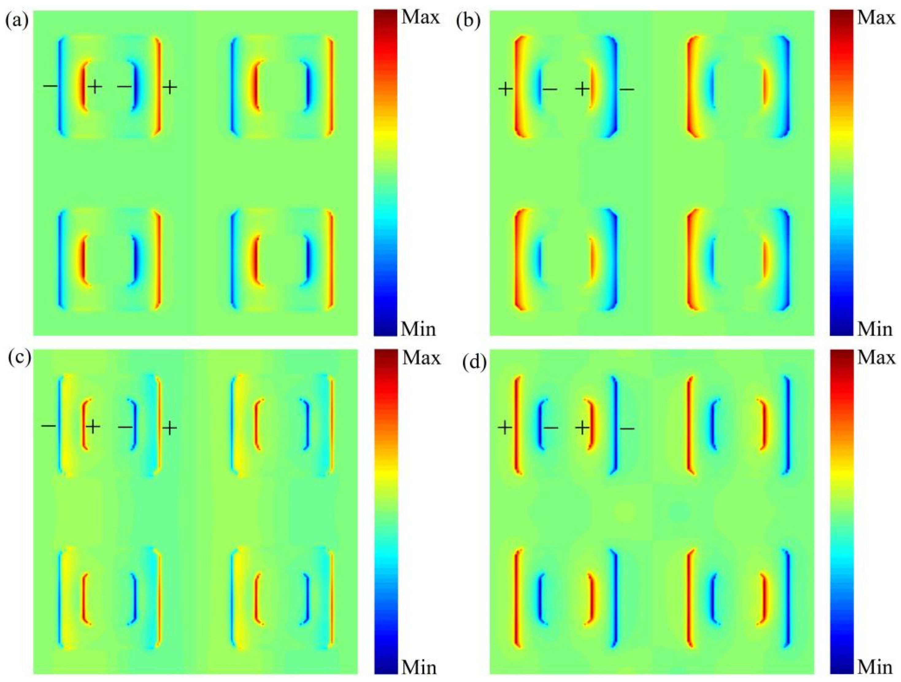
To better explain the absorption mechanism of the dual-broadband absorption, we analyze the electric field distribution at the absorption peak. Figure 6a,c shows the electric field distributions at Peak 1 and Peak 3 when the vanadium dioxide conductivity is S/m. The charge is distributed on the inner and outer sides of the vanadium dioxide in the form of “”, exhibiting the local plasmon resonance phenomenon. Similarly, as shown in Figure 6b,d, the electric fields at Peak 2 and Peak 4 exhibit local plasmon resonance, and the charges are distributed as “” on the inner and outer sides of the vanadium dioxide. It can be seen that the localized plasmon resonance is the main reason for the dual-broadband absorption of the absorber.
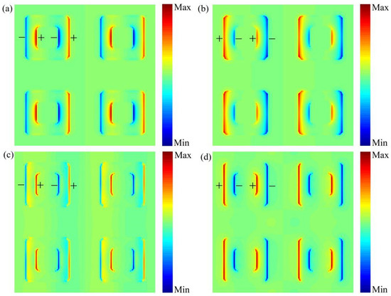
Figure 6.
Electric field distribution at (a) Peak 1 = 2.95 THz. (b) Peak 2 = 4.4 THz. (c) Peak 3 = 9.1 THz. (d) Peak 4 = 11.3 THz.
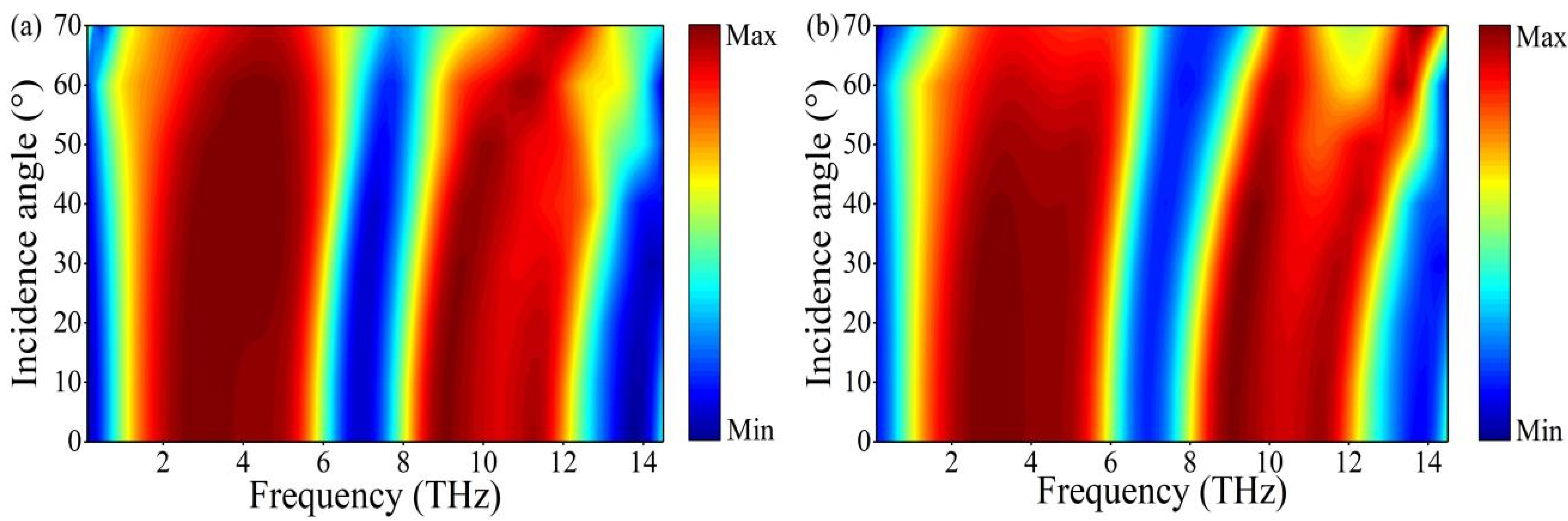
The angle at which the absorber maintains stable absorption under oblique incidence is an important parameter to measure whether the absorber can be applied in practice. Therefore, we investigated the effect of the incident angles of THz waves on the absorptance. Here, we set the conductivity of the vanadium dioxide to S/m and the thickness of the vanadium dioxide film to 0.81 µm. As shown in Figure 7a, the incident wave angle of TE polarization is increased from to , the two broadband absorptions are slightly blue-shifted and a stable absorption bandwidth is maintained in the to range. The high-frequency absorption bandwidth becomes narrower when the incident angle is greater than . The variation of the two broadband absorptions with the TM polarization angle is shown in Figure 7b. As the angle of incidence increases, the two broadband absorptions gradually blue-shift. The broadband absorption at high frequencies splits into two absorption peaks after incident angles greater than , but the absorptance can still remain above 90%. From the above discussion, we can conclude that the structure is a tunable, polarization insensitive and a wide-angle dual-broadband perfect THz wave absorber.
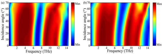
Figure 7.
Absorption spectra of the absorber for (a) TE and (b) TM polarization at different oblique incidence angles.
In recent years, many new metamaterial absorbers have been proposed one after another. The comparisons of the absorption bandwidth, adjustable material, tunable function and oblique incidence of the absorber with those of similar articles are shown in Table 1. Our designed absorber can actively tune the absorptance and absorption bandwidth using vanadium dioxide. Additionally, the width of the absorption bandwidth and the oblique incidence angle for maintaining a stable absorptance are higher than those in previous reports, so this metamaterial perfect absorber has broad application prospects in modulators, stealth and light-guided optical switches.

Table 1.
Comparison of this work with similar articles.
4. Conclusions
In summary, we propose and study an actively tunable dual-broadband terahertz perfect absorber, each cell of which is composed of four vanadium dioxide fillet cavities, a TOPAS dielectric spacer, a vanadium dioxide film, a SiO2 layer and gold film from top to bottom. The absorption bandwidth can reach 3.4 THz and 3.06 THz with absorptance higher than 90% and is insensitive to the polarization angle. The absorptance and absorption bandwidth can be continuously adjusted by changing the conductivity of the vanadium dioxide. In addition, this design enables stable broadband absorption of TE and TM polarizations within oblique incidence angles of and , respectively. The absorber may have a wide range of applications in THz devices such as modulators, cloaking devices and light-guided optical switches.
Author Contributions
Conceptualization, H.F. and Y.G.; software, H.F. and Y.G.; formal analysis, H.F., Z.Z., J.Z., D.F., J.W., C.L., T.W., G.W., L.W., L.R. and Y.G.; data curation, H.F. and Y.G.; writing—original draft preparation, H.F. All authors have read and agreed to the published version of the manuscript.
Funding
This research was funded by the Natural Science Foundation of Heilongjiang Province (Grant No. LH2019F047), the Project of the Central Government Supporting the Reform and Development of Local Colleges and Universities (Grant No. 2020YQ01), the Heilongjiang University Outstanding Youth Science Fund of Heilongjiang University (JCL201404), the Heilongjiang University Youth Science Fund Project (QL201301) and The Science and Technology Research Project of the Education Department of Heilongjiang Province (12541633).
Institutional Review Board Statement
Not applicable.
Informed Consent Statement
Not applicable.
Data Availability Statement
The data are included in the main text.
Conflicts of Interest
The authors declare no conflict of interest.
References
- Song, J.H.; Nagatsuma, T. Present and Future of Terahertz Communications. IEEE Trans. Terahertz Sci. Technol. 2011, 1, 256–263. [Google Scholar] [CrossRef]
- Federici, J.F.; Schulkin, B.; Huang, F.; Gary, D.; Barat, R.; Oliveira, F.; Zimdars, D. THz imaging and sensing for security applications-explosives, weapons and drugs. Semicond. Sci. Technol. 2005, 20, S266–S280. [Google Scholar] [CrossRef]
- Tonouchi, M. Cutting-edge terahertz technology. Nat. Photonics 2007, 1, 97–105. [Google Scholar] [CrossRef]
- Li, X.; Yang, L.; Hu, C.; Luo, X.; Hong, M. Tunable bandwidth of band-stop filter by metamaterial cell coupling in optical frequency. Opt. Express 2011, 19, 5283–5289. [Google Scholar] [CrossRef] [PubMed]
- Xiong, R.; Li, J. Double layer frequency selective surface for Terahertz bandpass filter. J. Infrared Millim. Terahertz Waves 2018, 39, 1039–1046. [Google Scholar]
- Xu, Z.C.; Gao, R.M.; Ding, C.F.; Zhang, Y.T.; Yao, J.Q. Multiband metamaterial absorber at terahertz frequencies. Chin. Phys. Lett. 2014, 31, 054205. [Google Scholar] [CrossRef]
- Song, Z.; Wang, Z.; Wei, M. Broadband tunable absorber for terahertz waves based on isotropic silicon metasurfaces. Mater. Lett. 2019, 234, 138–141. [Google Scholar] [CrossRef]
- Arik, K.; AbdollahRamezani, S.; Khavasi, A. Polarization insensitive and broadband terahertz absorber using graphene disks. Plasmonics 2017, 12, 393–398. [Google Scholar] [CrossRef]
- Danila, O. Polyvinylidene fluoride-based metasurface for high-quality active switching and spectrum shaping in the terahertz G-band. Polymers 2021, 13, 1860. [Google Scholar] [CrossRef]
- Danila, O.; Manaila-Maximean, D.; Barar, A.; Loiko, V.A. Non-layered Gold-Silicon and All-Silicon Frequency-Selective Metasurfaces for Potential Mid-Infrared Sensing Applications. Sensors 2021, 21, 5600. [Google Scholar] [CrossRef]
- Cong, L.; Cao, W.; Zhang, X.; Tian, Z.; Gu, J.; Singh, R.; Han, J.; Zhang, W. A perfect metamaterial polarization rotator. Appl. Phys. Lett. 2013, 103, 171107. [Google Scholar] [CrossRef]
- Gric, T.; Cada, M.; Pistora, J. Propagation of surface waves formed at the interface between hyperbolic metamaterial and highly doped semiconductor. Opt. Quantum Electron. 2016, 48, 237. [Google Scholar] [CrossRef]
- Liu, X.L.; Starr, T.; Starr, A.F.; Padilla, W.J. Infrared spatial and frequency selective metamaterial with near-unity absorbance. Phys. Rev. Lett. 2010, 104, 207403. [Google Scholar] [CrossRef] [PubMed] [Green Version]
- Campbell, S.D.; Grobe, S.D.; Goodin, I.L.; Su, Q.; Grobe, R. Limitations of decomposition-based imaging of longitudinal absorber confifigurations. Phys. Rev. A 2008, 77, 023821. [Google Scholar] [CrossRef] [Green Version]
- Ni, X.; Wong, J.Z.; Mrejen, M.; Wang, Y.; Zhang, X. An ultrathin invisibility skin cloak for visible light. Science 2015, 349, 1310–1314. [Google Scholar] [CrossRef]
- Schurig, D.; Mock, J.J.; Justice, B.J.; Cummer, S.A.; Pendry, J.B.; Starr, A.F.; Smith, D.R. Metamaterial electromagnetic cloak at microwave frequencies. Science 2006, 314, 977–980. [Google Scholar] [CrossRef] [Green Version]
- Atwater, H.A.; Polman, A. Erratum: Plasmonics for improved photovoltaic devices. Nat. Mater. 2010, 9, 205–213. [Google Scholar] [CrossRef]
- Wang, Y.; Sun, T.; Paudel, T.; Zhang, Y.; Ren, Z.; Kempa, K. Metamaterial-plasmonic absorber structure for high efficiency amorphous silicon solar cells. Nano Lett. 2012, 12, 440–445. [Google Scholar] [CrossRef]
- Danila, O.; Manaila-Maximean, D. Bifunctional Metamaterials Using Spatial Phase Gradient Architectures: Generalized Reflection and Refraction Considerations. Materials 2021, 14, 2201. [Google Scholar] [CrossRef]
- Landy, N.I.; Sajuyigbe, S.; Mock, J.J.; Smith, D.R.; Padilla, W.J. Perfect Metamaterial Absorber. Phys. Rev. Lett. 2008, 100, 207402. [Google Scholar] [CrossRef]
- Bai, J.; Zhang, S.; Fan, F.; Wang, S.; Sun, X.; Miao, Y.; Chang, S. Tunable broadband THz absorber using vanadium dioxide metamaterials. Opt. Commun. 2019, 452, 292–295. [Google Scholar] [CrossRef]
- Tao, H.; Landy, N.I.; Bingham, C.M.; Zhang, X.; Averitt, R.D.; Padilla, W.J. A metamaterial absorber for the terahertz regime: Design, fabrication and characterization. Opt. Express 2008, 16, 7181–7188. [Google Scholar] [CrossRef] [PubMed]
- Wu, T.; Shao, Y.; Ma, S. Broadband terahertz absorber with tunable frequency and bandwidth by using Dirac semimetal and strontium titanate. Opt. Express 2021, 29, 7713–7723. [Google Scholar] [CrossRef] [PubMed]
- Cen, C.; Liu, L.; Zhang, Y.; Chen, X.; Xiao, S. Tunable absorption enhancement in periodic elliptical hollow graphene arrays. Opt. Mater. Express 2019, 9, 706–716. [Google Scholar] [CrossRef]
- Huang, J.; Li, J.; Yang, Y.; Li, J.; Zhang, Y.; Yao, J. Active controllable dual broadband terahertz absorber based on hybrid metamaterials with vanadium dioxide. Opt. Express 2020, 28, 7018–7027. [Google Scholar] [CrossRef]
- Jiao, X.F.; Zhang, Z.H.; Li, T. Tunable Dual Broadband Terahertz Metamaterial Absorber Based on Vanadium Dioxide. Appl. Sci. 2020, 10, 7259. [Google Scholar] [CrossRef]
- Zhang, J.; Tian, J.; Li, L. A dual-band tunable metamaterial near-unity absorber composed of periodic cross and disk graphene arrays. IEEE Photonics J. 2018, 10, 4800512. [Google Scholar] [CrossRef]
- Tao, H.; Bingham, C.M.; Pilon, D.; Fan, K.; Strikwerda, A.C.; Shrekenhamer, D.; Padilla, W.J.; Zhang, X.; Averitt, R.D. A dual band terahertz metamaterial absorber. J. Phys. D Appl. Phys. 2010, 43, 225102. [Google Scholar] [CrossRef]
- Bao, Z.; Wang, J.; Hu, Z.D.; Balmakou, A.; Zhang, C. Coordinated multi-band angle insensitive selection absorber based on graphene metamaterials. Opt. Express 2019, 27, 31435–31445. [Google Scholar] [CrossRef]
- Xu, K.D.; Li, J.; Zhang, A.; Chen, Q. Tunable multi-band terahertz absorber using single-layer square graphene ring structure with T-shaped graphene strips. Opt. Express 2020, 28, 11482–11492. [Google Scholar] [CrossRef]
- Hu, F.; Wang, H.; Zhang, X.; Xu, X.; Jiang, W.; Rong, Q.; Zhao, S.; Jiang, M.; Zhang, W.; Han, J. Electrically triggered tunable terahertz band-pass filter based on VO2 hybrid metamaterial. IEEE J. Sel. Top. Quantum Electron. 2019, 25, 4700207. [Google Scholar] [CrossRef]
- Li, Q.; Liu, S.; Zhang, X.; Wang, S.; Chen, T. Electromagnetically induced transparency in terahertz metasurface composed of meanderline and U-shaped resonators. Opt. Express 2020, 28, 8792–8801. [Google Scholar] [CrossRef] [PubMed]
- Liu, L.; Kang, L.; Mayer, T.S.; Werner, D.H. Hybrid metamaterials for electrically triggered multifunctional control. Nat. Commun. 2016, 7, 13236. [Google Scholar] [CrossRef] [PubMed]
- Wen, Q.; Zhang, H.; Yang, Q.; Xie, Y.; Chen, K.; Liu, Y. Terahertz metamaterials with VO2 cut-wires for thermal tunability. Appl. Phys. Lett. 2010, 97, 021111. [Google Scholar] [CrossRef]
- Liu, J.; Fan, L. Development of a tunable terahertz absorber based on temperature control. Microw. Opt. Technol. Lett. 2020, 62, 1681–1685. [Google Scholar]
- Choi, S.B.; Kyoung, J.S.; Kim, H.S.; Park, H.R.; Park, D.J.; Kim, B.J.; Ahn, Y.H.; Rotermund, F.; Kim, H.T.; Ahn, K.J.; et al. Nanopattern enabled terahertz all-optical switching on vanadium dioxide thin film. Appl. Phys. Lett. 2011, 98, 071105. [Google Scholar] [CrossRef]
- Zhang, Y.; Qiao, S.; Sun, L.; Shi, Q.; Huang, W.; Li, L.; Yang, Z. Photoinduced active terahertz metamaterials with nanostructured vanadium dioxide film deposited by sol-gel method. Opt. Express 2014, 22, 11070–11078. [Google Scholar] [CrossRef]
- Zheng, Z.P.; Zheng, Y.; Luo, Y.; Yi, Z.; Liu, L.; Song, Q.J.; Wu, P.H.; Yu, Y.; Zhang, J.F. Terahertz perfect absorber based on flexible active switching of ultra-broadband and ultra-narrowband. Opt. Express 2021, 29, 42787–42799. [Google Scholar] [CrossRef]
- Zhang, M.; Song, Z. Switchable terahertz metamaterial absorber with broadband absorption and multiband absorption. Opt. Express 2021, 29, 21551–21561. [Google Scholar] [CrossRef]
- Lv, T.; Dong, G.; Qin, C.; Qu, J.; Shi, J.H. Switchable dual-band to broadband terahertz metamaterial absorber incorporating VO2 phase transition. Opt. Express 2021, 29, 5437–5447. [Google Scholar] [CrossRef]
- Zhu, H.; Zhang, Y.; Ye, L. Switchable and tunable terahertz metamaterial absorber with broadband and multi-band absorption. Opt. Express 2020, 28, 38626–38637. [Google Scholar] [CrossRef] [PubMed]
- Gric, T.; Eldlio, M.; Cada, M.; Pistora, J. Analytic solution to field distribution in two-dimensional inhomogeneous waveguides. J. Electromagn. Waves Appl. 2015, 29, 1068–1081. [Google Scholar] [CrossRef]
- Song, Z.; Deng, Y.; Zhou, Y.; Liu, Z. Terahertz toroidal metamaterial with tunable properties. Opt. Express 2019, 27, 5792–5797. [Google Scholar] [CrossRef] [PubMed]
- Wang, S.; Kang, L.; Werner, D.H. Hybrid resonators and highly tunable terahertz metamaterials enabled by vanadium dioxide (VO2). Sci. Rep. 2017, 7, 4326. [Google Scholar] [CrossRef]


Publisher’s Note: MDPI stays neutral with regard to jurisdictional claims in published maps and institutional affiliations. |
© 2022 by the authors. Licensee MDPI, Basel, Switzerland. This article is an open access article distributed under the terms and conditions of the Creative Commons Attribution (CC BY) license (https://creativecommons.org/licenses/by/4.0/).