Article

Photoelectrochemical Enhancement of Graphene@WS2 Nanosheets for Water Splitting Reaction

1
Laboratory of Physics of Condensed Matter, University of Picardie Jules Verne, Scientific Pole, 33 Rue Saint-Leu, CEDEX 1, 80039 Amiens, France
2
Solid-State Physics Department, Physics Research Institute, National Research Centre, 33 El-Bohouth Street, Dokki, Giza 12622, Egypt
3
Advanced Materials Research Center, Technology Innovation Institute, Abu Dhabi P.O. Box 9639, United Arab Emirates
4
Aix Marseille University, Faculté des Sciences et Techniques, CP2M, IM2NP, Avenue Escadrille Normandie Niemen, 13397 Marseille, France
5
Laboratoire National de Métrologie et D’essais (LNE), 29 Avenue Roger Hannequin, 78197 Trappes, France
*
Author to whom correspondence should be addressed.
Nanomaterials 2022, 12(11), 1914; https://doi.org/10.3390/nano12111914
Submission received: 12 May 2022 / Revised: 26 May 2022 / Accepted: 31 May 2022 / Published: 3 June 2022

Abstract

:
Tungsten disulfide nanosheets were successfully prepared by one-step chemical vapor deposition using tungsten oxide and thiourea in an inert gas environment. The size of the obtained nanosheets was subsequently reduced down to below 20 nm in width and 150 nm in length using high-energy ball milling, followed by 0.5 and 1 wt% graphene loading. The corresponding vibrational and structural characterizations are consistent with the fabrication of a pure WS2 structure for neat sampling and the presence of the graphene characteristic vibration modes in graphene@WS2 compounds. Additional morphological and crystal structures were examined and confirmed by high-resolution electron microscopy. Subsequently, the investigations of the optical properties evidenced the high optical absorption (98%) and lower band gap (1.75 eV) for the graphene@WS2 compared to the other samples, with good band-edge alignment to water-splitting reaction. In addition, the photoelectrochemical measurements revealed that the graphene@WS2 (1 wt%) exhibits an excellent photocurrent density (95 μA/cm2 at 1.23 V bias) compared with RHE and higher applied bias potential efficiency under standard simulated solar illumination AM1.5G. Precisely, graphene@WS2 (1 wt%) exhibits 3.3 times higher performance compared to pristine WS2 and higher charge transfer ability, as measured by electrical impedance spectroscopy, suggesting its potential use as an efficient photoanode for hydrogen evolution reaction.

1. Introduction

Hydrogen fuel is considered a promising source of clean energy that could partly replace fossil fuels at the origin of greenhouse gas emissions. Today, there is a growing universal tendency to focus research and development on green hydrogen production by considering the general ecosystem to lower its costs and make it a more affordable clean-energy source, especially through water splitting (WS) [1,2,3,4,5]. In this context, several advanced materials were successfully examined and tested for enhancing the WS reaction, such as noble metals combined with highly catalytic semiconductors, which have shown an improved hydrogen evolution reaction (HER). However, their complex implementation and high cost prohibited their adoption in realistic WS plants [6,7,8,9]. Therefore, cost-efficient and easy-to-produce alternative materials with improved WS performances have attracted a great interest. To this end, WS2, a transition-metal dichalcogenide (TMD) semiconductor, constitutes a highly attractive option owing to its excellent band gap tunability, its stability at high temperatures in corrosive media, and its easy and low-cost fabrication. Recently, both computational and experimental studies carried out on WS2 have shown its effective role in catalyzing HER with a relatively good yield [10,11,12,13,14,15,16]. WS2-like materials, such as vertically aligned MoS2, have shown increasingly exposed edges as active sites for HER electrocatalysis, while the basal plane is catalytically inert [17]. The increasing interest in using TMDs as supporting electrodes is justified by their easy and low-cost process [15,18,19,20]. To further improve WS2 performances, it is crucial to select an appropriate catalyst-supporting material that can prevent high-surface-area WS2 nanostructures from agglomerating, enhance electron mobility, and overcome the surface overpotential to improve the overall HER performance. Graphene is the other two-dimensional carbon material that would meet the aforementioned criteria. Due to its high ability in electronic excitation and mobility, its mechanical properties, and its high stability, even at the nanoscale, graphene has received rigorous scientific and industrial attention for a long time [21,22,23,24,25,26]. Indeed, graphene is reported to possess high specific surface area (~2600 m2/g), high electron mobility μe at room temperature (250,000 cm2/Vs), outstanding thermal conductivity (5000 W m−1 K−1), and high electrical conductivity (5:6.4 × 10⁶ S/m), as well as a very low weight. These outstanding proprieties enable graphene to be considered an excellent electrocatalyst support for WS2 nanostructures [21,22].
In this work, we first produced low-cost graphene@WS2 nanocomposite as electrodes for improved WS reactions. Next, we conducted a systematic structural characterization and assessment of the optical properties to evaluate the performance of the fabricated samples in photocatalysis-driven WS.

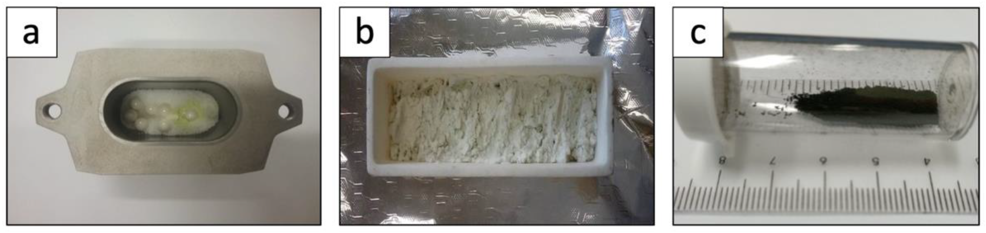
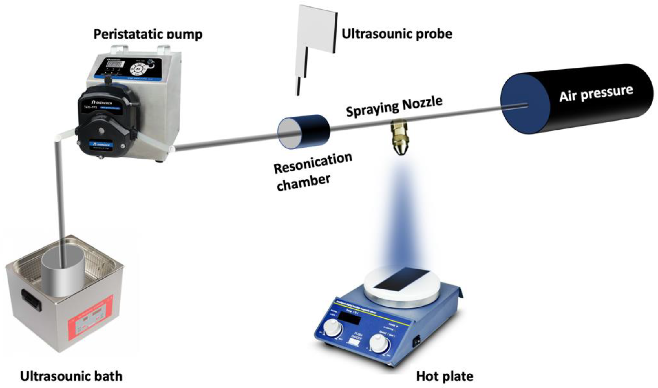
2. Materials and Methods

The raw materials, namely tungsten oxide (WO3) and thiourea (CH4N2S) powders, were acquired from Alfa Aesar™ (Thermo Fisher GmbH, Kandel, Germany). Graphene nanoplatelets were purchased from Sigma Aldrich™ St. Louis, MO, USA. The indium tin oxide (ITO) substrates used in this study are from Lumtec™ (Tapei, Taiwan), exhibiting a resistance < 10 Ω/cm2. All used substrates were cleaned by immersion in detergent, rinsed successively with acetone, ethanol, and deionized water, and dried under nitrogen flow. WS2 nanosheets were prepared using four processing conditions consisting of various WO3 and thiourea contents until achieving the complete suppression of the oxygen residue and obtaining pure WS2 nanosheets. The initial materials’ contents and the corresponding samples are summarized in the Table 1.
In a typical processing route, WS2 nanosheets are prepared by mixing WO3 with thiourea using a high-energy ball milling process E-Max Retsh™ (GmbH, Düsseldorf, Germany) machine with tungsten carbide container and Zirconia oxide balls (Figure 1a). After milling at 400 rpm for 30 min, the obtained mixture was collected into 50 mL alumina crucible (Figure 1b). A tube furnace was used for the chemical vapor deposition (CVD) reaction. The processing temperature was set to 850 °C under nitrogen gas flow of 500 sccm at 20 °C/s heating rate. The mixture was introduced into the tube furnace at T = 400 °C, and the CVD reaction took place for 1 h of dwell time at 850 °C, followed by air cooling. The obtained WS2 exhibited its typical black color (Figure 1c).
The chemical reaction occurring during the CVD process is expressed as follows:
WO 3   + 2 ( CH 4 N 2 S ) Δ N 2   WS 2   + 2 ( CH 4 N 2 ) +   O 3 ,
For the graphene@WS2 nanocomposites, two graphene contents (0.5 wt% and 1 wt%) were added to the optimized fabricated WS2 nanosheets (S4), followed by high-energy ball milling at 400 rpm for 1 h. To investigate the different physical properties of the resulting compounds, thin films were prepared on top of various substrates, such as glass, quartz, and ITO. Figure 2 shows an illustration of the enhanced spray technique, where two ultrasonic-solution dispersive devices were utilized to prevent WS2 nanosheets from aggregating in the transferring tube. Ethanol was used as the host solution.
For all samples, the spraying procedure consisted of 0.1 g of a mixture made of WS2 with or without graphene, which was poured into a 40-megaliter ethanol container followed by water-bath sonication, as shown in Figure 2. During the solution distribution through a peristatic pump, a second sonication (ultrasound probe) was used to resuspend the mixture towards the nozzle. Finally, an air pressure of 1.2 bar allowed spraying the dispersed suspension though a nozzle over the desired substrate, which was kept at 45 °C with a hot plate. The nozzle–substrate distance was maintained at 20 cm and the deposition rate was set to 1 mL/min for a total deposition time of 30 min. The obtained film thickness was in the range of 150 to 200 nm.
Subsequently, the structural characterization was carried out using a Bruker™ D4 Endeavor X-ray diffractometer with a 1.54 Å CuKα source, and the vibrational analyses were performed with Raman spectroscopy Renishaw™ ( Wotton-under-Edge, UK) using a green laser excitation source (532 nm). The microstructure analysis was performed with a Zeiss™ (Oberkochen, Germany) Gemini 500 ultra-high resolution field emission electron microscope (FESEM) operating at low voltage (1 kV), using an In-lens detector. The crystal structure and the morphology of the obtained nanocomposite were investigated by high-resolution transmission electron microscopy (HRTEM) Cs-corrected Titan from Thermo Fisher Scientific™ (Waltham, MA, USA) operating at 300 kV. TEM samples were prepared on holey carbon Cu grids using drop-casting method. The analysis of optical properties was conducted on a UV-vis-near IR spectrometer V-700 JASCO™ (Easton, MD, USA) and Fourier transform infrared spectroscopy (FTIR) from Thermo Fisher Scientific™ (Waltham, MA, USA). The electrical impedance spectroscopy (EIS) and the photoelectrochemical (PEC) measurements were performed using PalmSens4™ (Houten, Netherlands) EIS electrochemical interface.

3. Results and Discussion

3.1. XRD Analysis

The XRD diagrams obtained for the four prepared WS2 samples are shown in Figure 3. The XRD patterns were recorded in the range of 2-theta 10–80° and compared to the observed reflection planes (002), (101), (102), (103), (110) and (203) with the standard diffraction data file (JCPDF card no. 01-084-1398). These diffraction peaks were indexed with the hexagonal WS2 phase of cell constants a = b = 3.15 Å, c = 12.32 Å.
The XRD diagrams of the samples S1, S2, and S3 exhibit an extra peak at (002) position which corresponds to the WO3 structure. This indicates that the reaction of the WO3 with the thiourea was not complete; hence, the resulting WS2 of these samples contained WO3 residue. It is worth noting that the strength of the WO3 residue peak was observed to decrease with increasing thiourea content (from sample S1 to S3). By contrast, the WO3 peak was no longer visible at higher thiourea content as it disappeared for the sample S4. This result suggests that the excess thiourea added to the mixture made it possible to obtain the pure WS2 nanosheets.

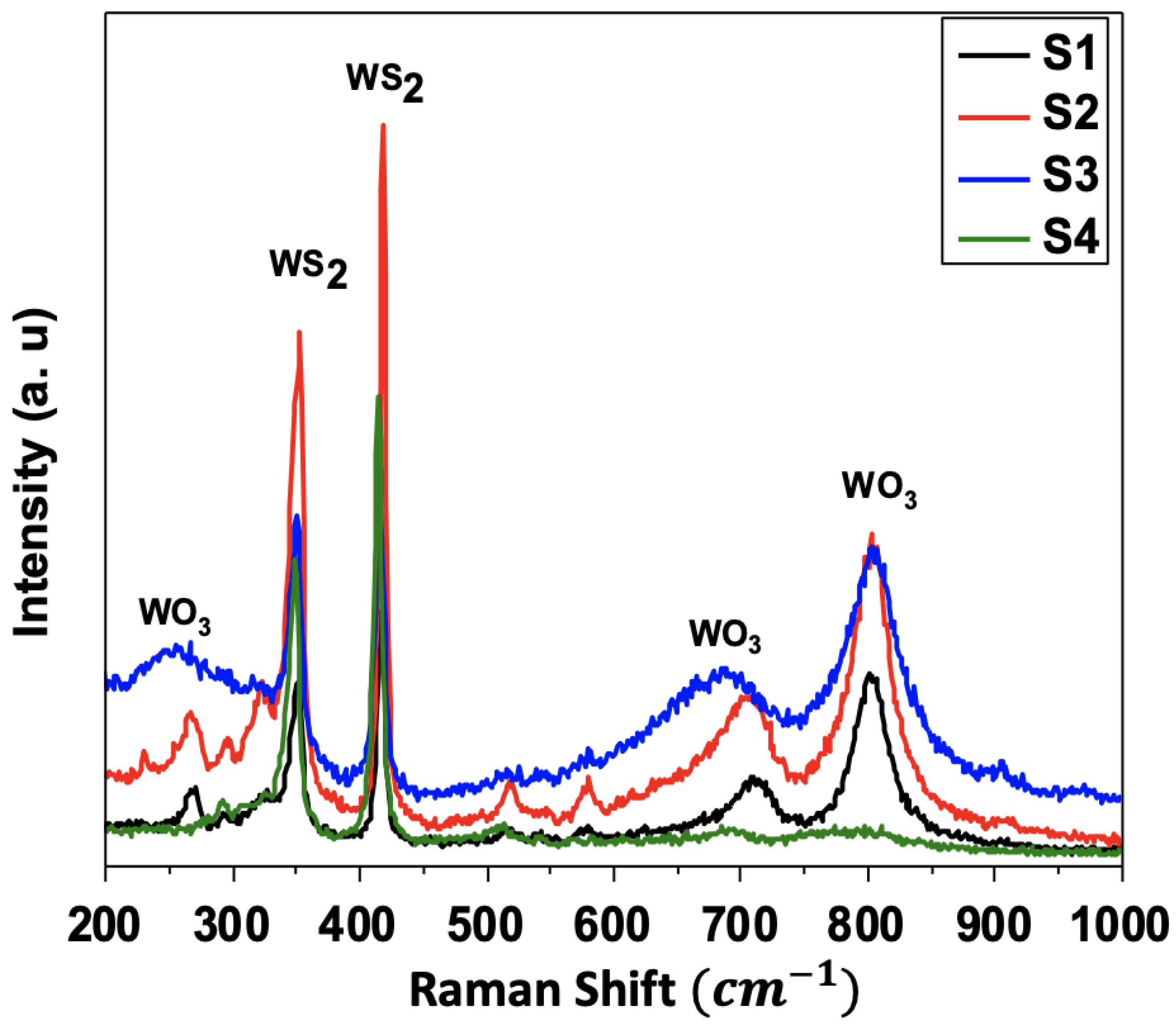
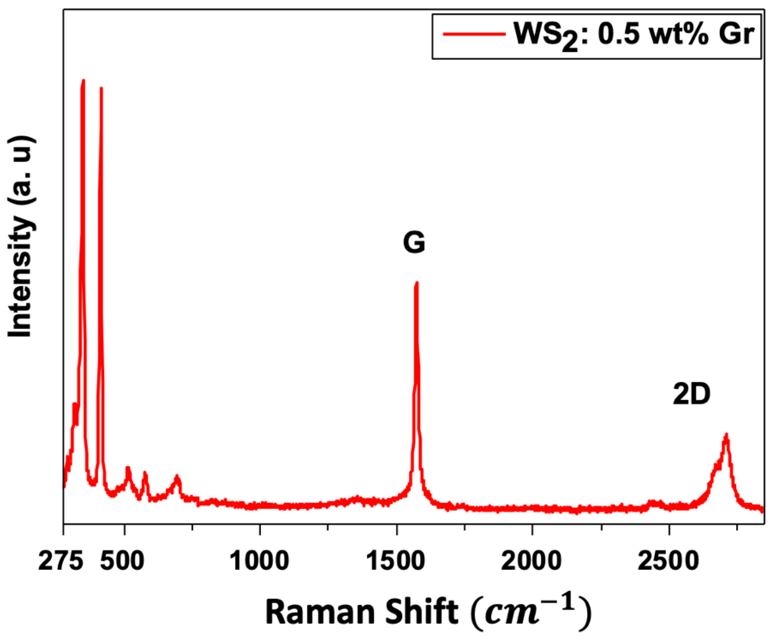
3.2. Raman Spectroscopy

Figure 4 illustrates the vibrational modes of the four processed WS2 samples. All the samples show common WS2 characteristic peaks, i.e., two strong peaks attributed to E2g1 in-plane and A1g out-of-plane vibrational modes appearing at the 350 and 420 cm−1 positions, respectively. The E2g1 mode involves a displacement of W and S atoms, whereas the A1g mode concerns only the S atoms.
Similar to the XRD results, the Raman spectra of the S1, S2, and S3 showed the presence of WO3 vibration modes at the 293 cm−1, 675 cm−1, and 836 cm−1 positions, respectively, while the S4 only exhibited the vibration modes E12g and A1g for WS2 occurring at 351 cm−1 and 415 cm−1, respectively. As mentioned above, these results confirm that the CVD reaction was fully completed for the S4 and the oxygen was entirely consumed.
Furthermore, the Raman spectroscopy was carried out on graphene@WS2 samples, and the typical Raman spectra are depicted in Figure 5. In addition to the presence of the common WS2 peaks, graphene vibrational modes were also obtained for both samples at 1560–1575 cm−1 and at 2647–2700 cm−1 for the G-band and 2D-band, respectively. This confirms the presence of the graphene in the processed graphene@WS2 samples.

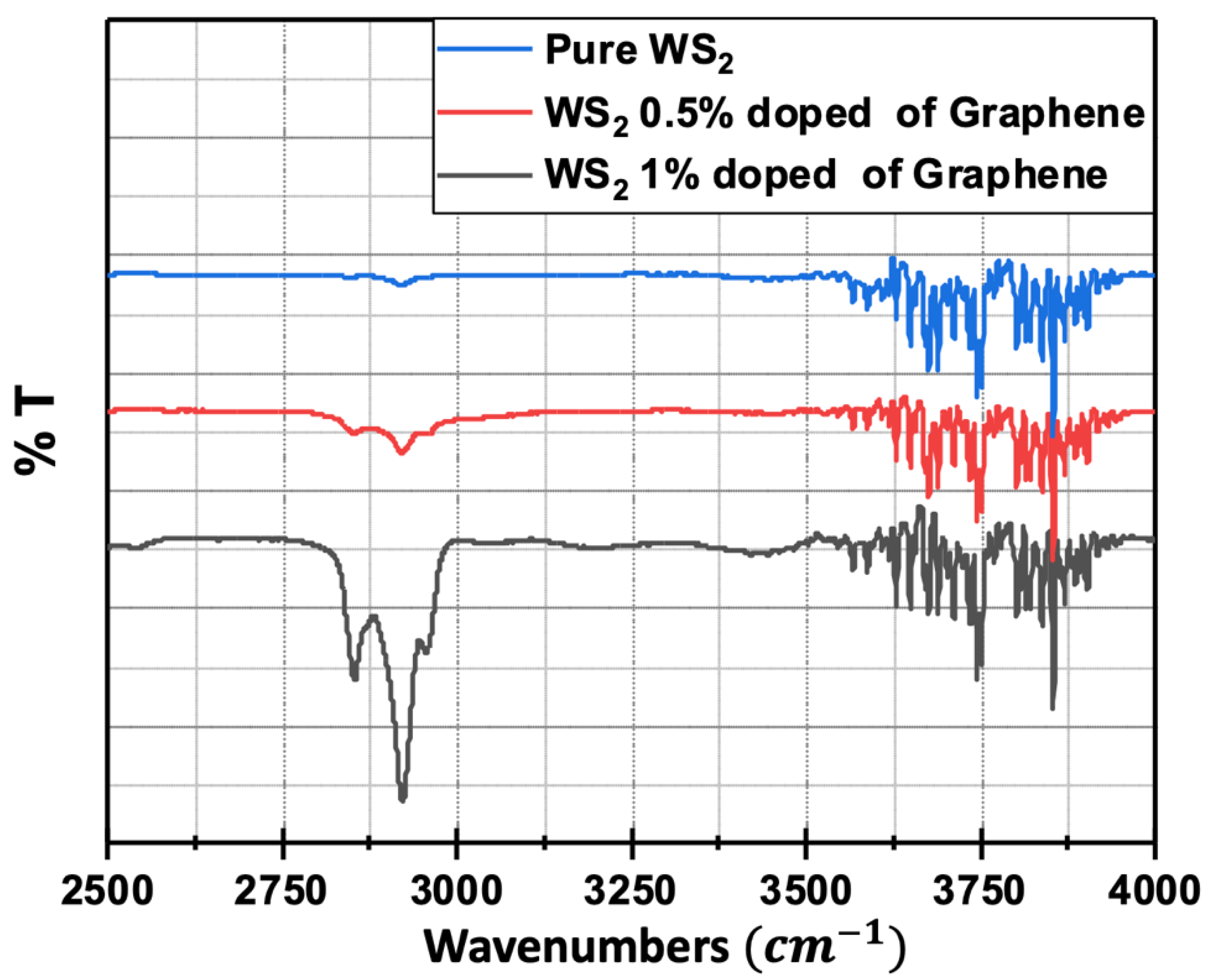
3.3. FTIR Spectroscopy

To further screen the presence of the graphene in the processed graphene@WS2 nanocomposite samples, FTIR absorption spectroscopy was conducted on pure WS2, WS2: 0.5 wt% Gr, and WS2: 1 wt% Gr, respectively, as shown in Figure 6.
As can be seen, the typical graphene absorption peak is present in the graphene@WS2 nanocomposites and the strength of this peak is more pronounced for the sample with the higher graphene content.

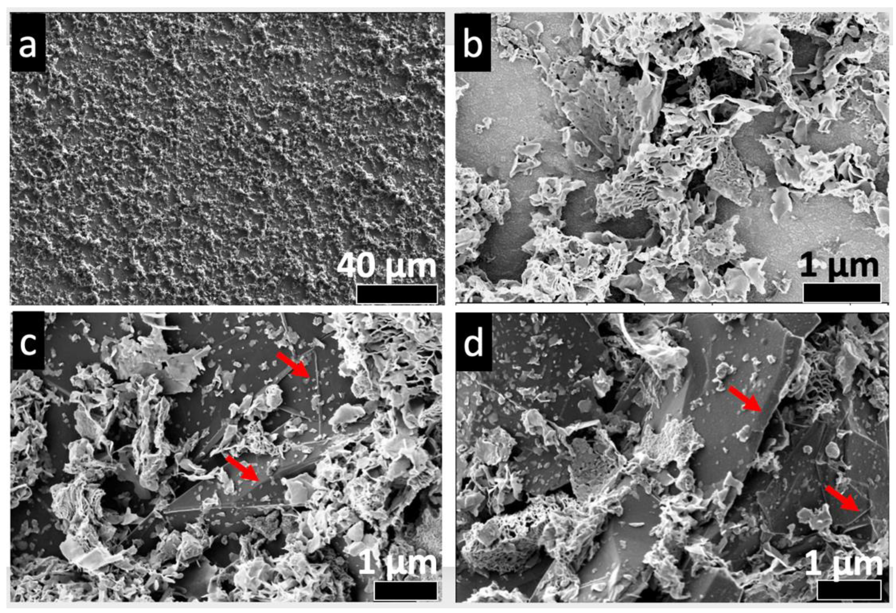
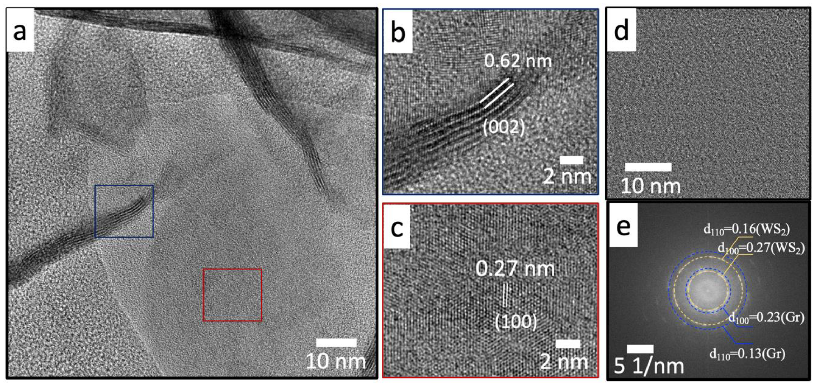
3.4. Microstructure Analysis

A general view of the sprayed samples on the ITO substrate is given in Figure 7a. As can be seen, the nanosheets are evenly distributed with relatively uniform thickness. The insets shown in Figure 7b–d highlight the inner structures of the neat WS2, WS2: 0.5 wt% Gr, and WS2: 1 wt% Gr, respectively. Both the WS2 nanosheets and the graphene platelets are visible. These samples were further investigated by HRTEM and used for the photoelectrochemical measurements.
Figure 8 depicts the bright-field TEM image of the typical microstructure encountered in WS2: 1 wt% Gr. The WS2 nanosheets (dark contrast) appeared to be encapsulated in the graphene nanoplatelets (light contrast), as shown in Figure 8a. A higher-magnification TEM image is given in Figure 8b; it shows a focus on entangled graphene@WS2 nanosheets. The quality of the nanocomposite was further verified using HRTEM.
Figure 9a clearly shows the interconnections between the WS2 nanosheets and the graphene nanoplatelets, delimited by the blue box highlighted in Figure 9b. Their corresponding crystal structure conformed with the 2H-WS2 materials, as demonstrated by the interplanar distances d(002) = 0.62 nm and d(100) = 0.27 nm, illustrated in the red box in Figure 9c. The analysis of the interconnected WS2 and graphene regions given in Figure 9d revealed the presence of both graphene and WS2, as demonstrated by the corresponding fast Fourier transform (FFT) intensity image depicted in Figure 9e.

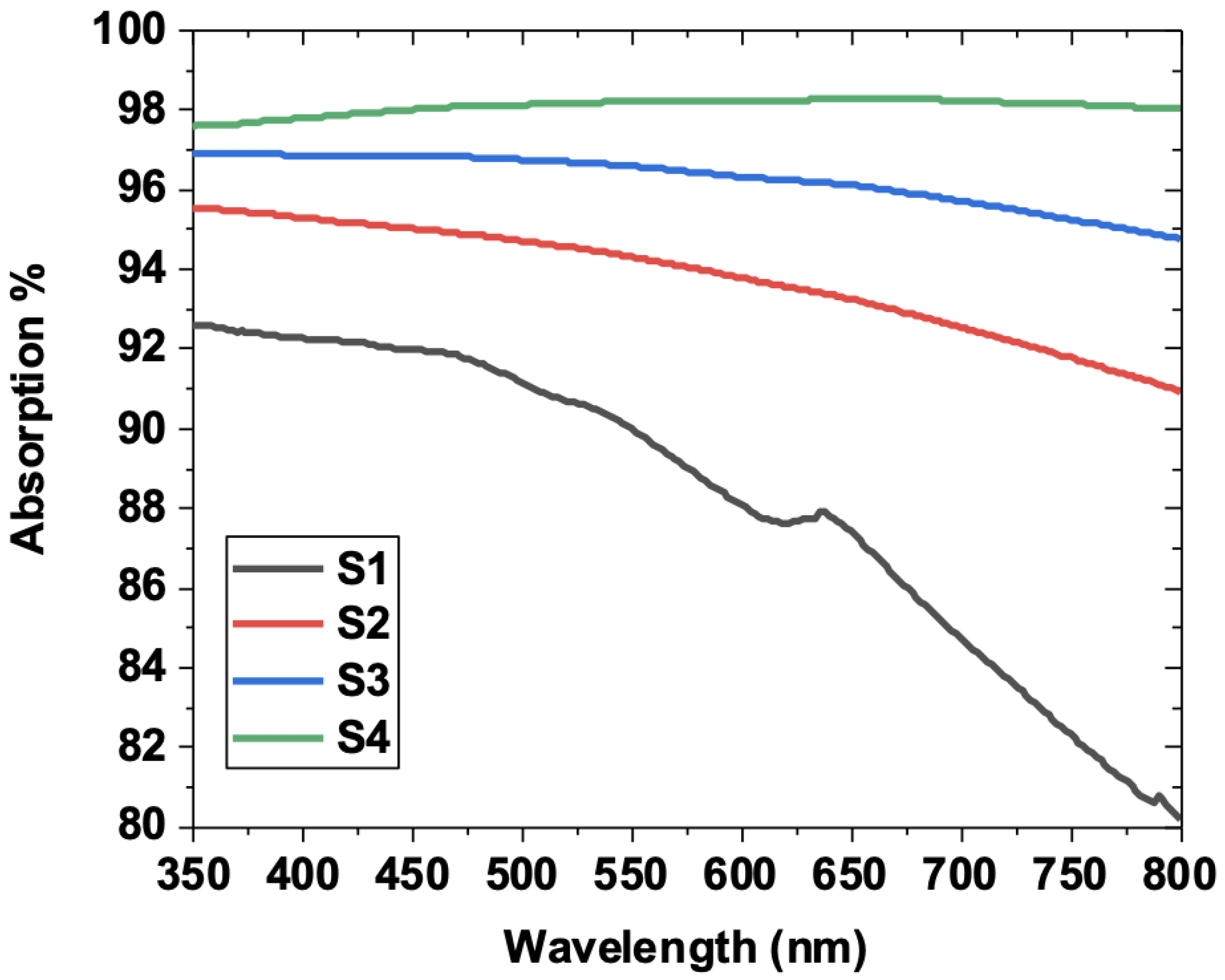
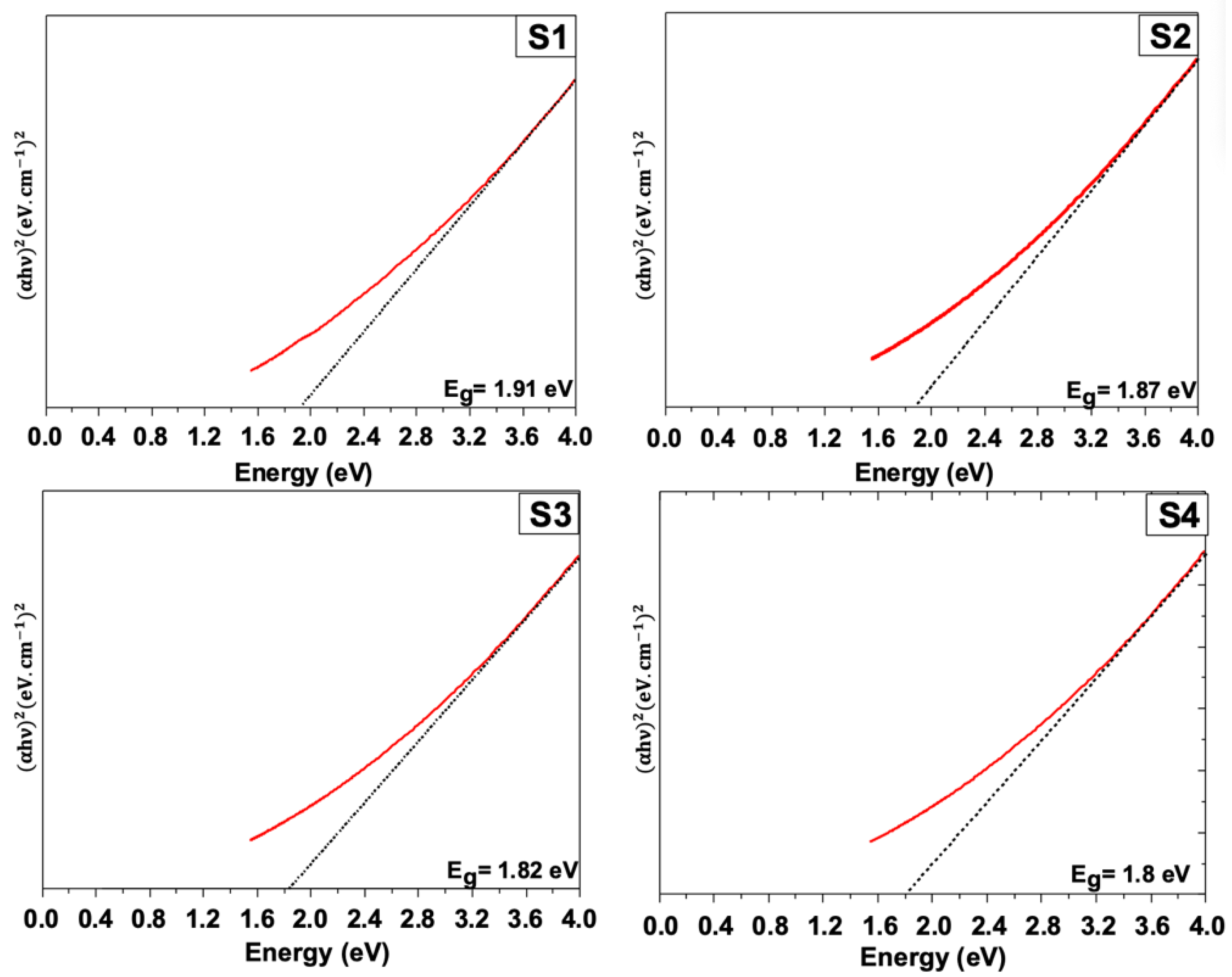
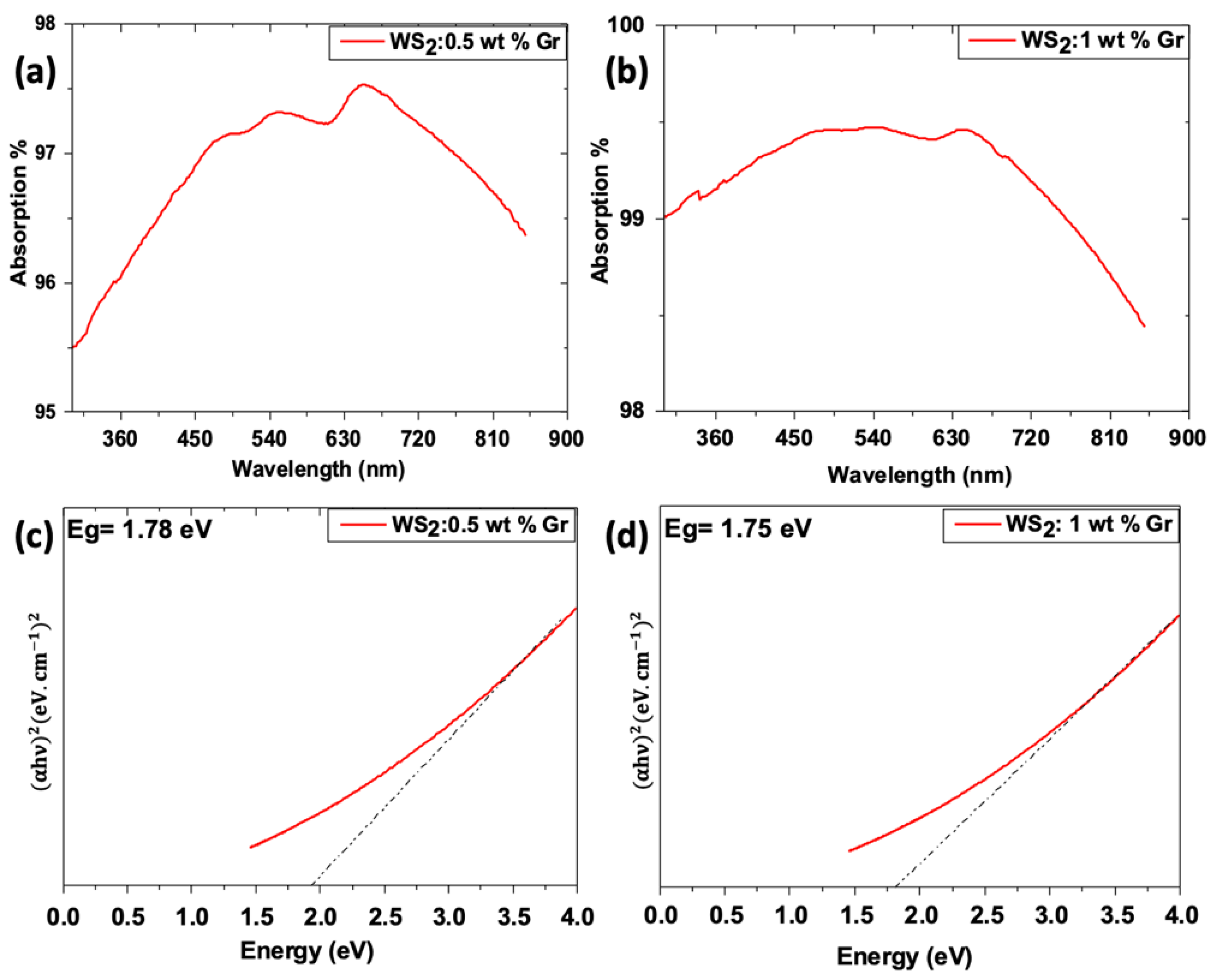
3.5. Optical Properties

The investigation of the optical properties was carried out using an optical spectrometer in the 350–800 nm range. Figure 10 shows the optical absorption of all the considered samples.
As can be seen, samples S1, S2, and S3 exhibited similar optical behavior, consisting of a steady decrease in the optical absorption, which started at 93–97% and hit 80% for S1. This suggests that the presence of WO3 impurities induces a decrease in the optical absorption in the visible region. By contrast, the optimized sample S4 showed a relatively unchanged optical absorption. In particular, it remained stable until it reached the excitons position (around 620 nm), at which point it slightly increased. It is clear that the optimized WS2 sample S4 exhibited high broadband light absorption in the visible region, reaching more than 98% compared to the other samples. Using the Tauc formula (αhυ)n = A(hϑ − Eg), the band-gap energy was obtained, as depicted in Figure 11.
The obtained band-gap energies were 1.91 eV, 1.87 eV, 1.82 eV, and 1.8 eV for S1, S2, S3, and S4, respectively. The S4 showed the lowest energy, which was in agreement with the broadband optical absorption performances achieved.
To evaluate the effect of the graphene’s incorporation on the WS2 nanosheets, the optical absorption was also measured for both graphene@WS2 samples, namely 0.5 wt% Gr and 1 wt% Gr, and the results are shown in Figure 12.
The addition of WS2: 0.5 wt% Gr does not seem to enhance the optical absorption (Figure 10 vs. Figure 12a). Indeed, the optical absorption of this sample reaches 98% absorption but only in the 550–750 nm region in contrast to pristine WS2, which exhibits a broadband absorption. Nevertheless, the WS2: 0.5 wt% Gr band gap energy appears to slight decrease to 1.78 eV (Figure 12c). In contrast, the WS2: 1 wt% Gr sample does exhibit an optical absorption exceeding 99% across the entire visible light spectrum. Moreover, its band gap energy is further decreased to reach 1.75 eV. Considering these performances, WS2 and WS2: 1 wt% Gr samples were selected to perform photochemical measurements.

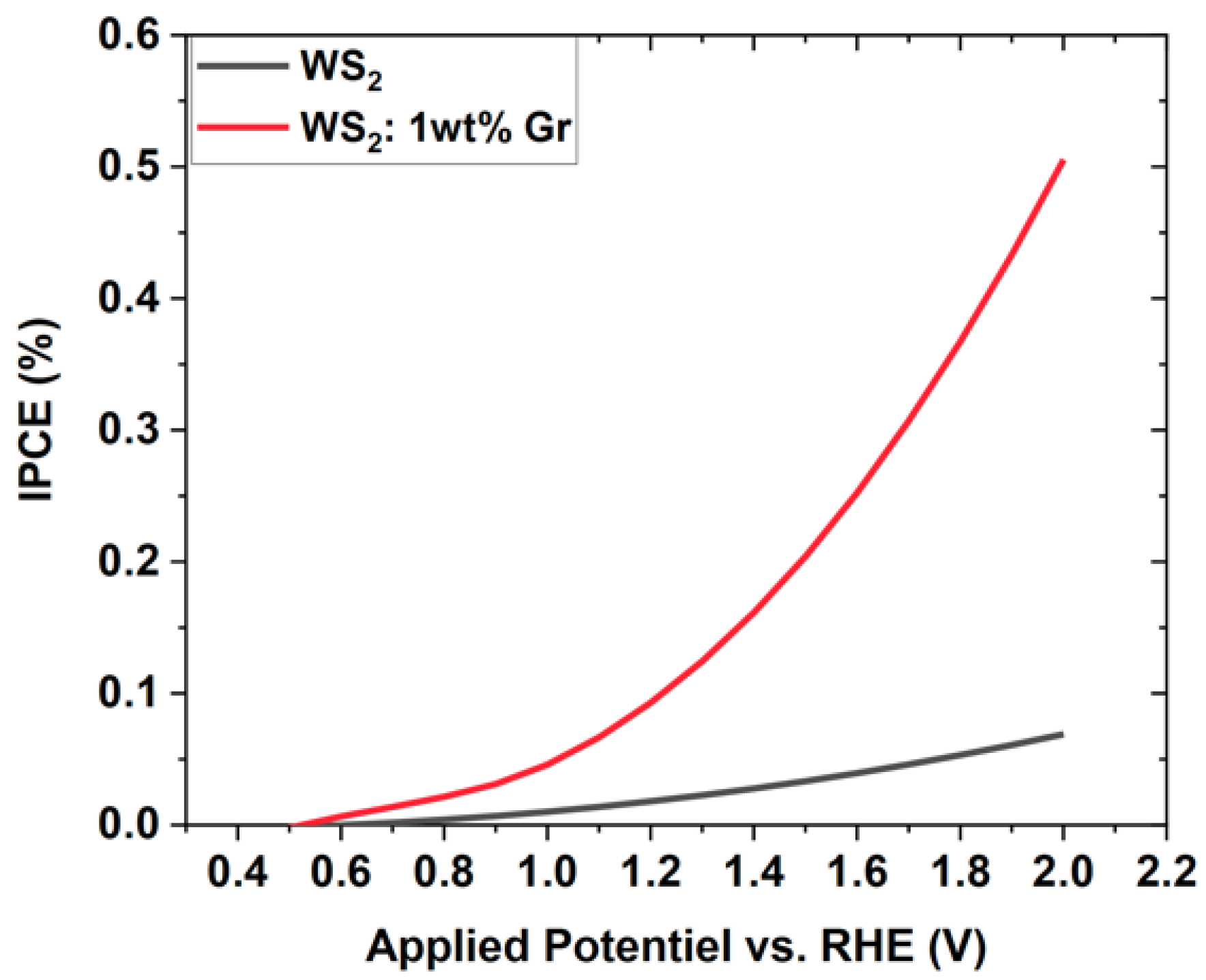
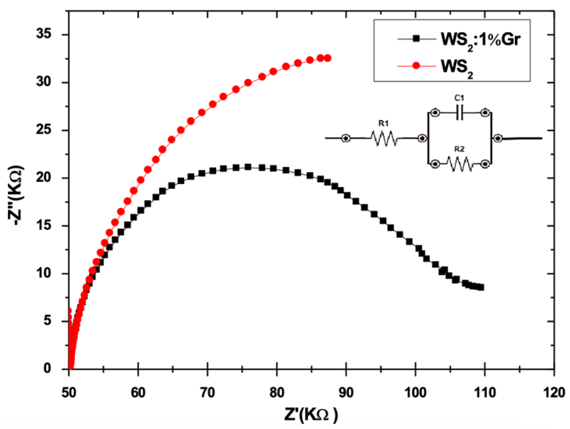
3.6. Photochemical Measurements

In this section, the photocatalytic performances of neat WS2 and WS2: 1 wt% Gr samples are screened. Both samples were deposited on ITO substrate and immersed in deionized water medium (pH = 6). Then, a linear sweep voltammetry (LSV) and chronoamperometry experiments were carried under standard solar simulator (energy~AM1.5G).
To extract the potential of RHE, the following Nernst equation was used:
E RHE = E ( Ag / AgCl ) + ( 0.059 ×   pH ) + E 0
where E0 ≈ 0.197 V at 25 °C and EAg/AgCl is the applied potential.
For both samples, the active surface is about 1 cm2 and the distance between the three electrodes was kept at 5 mm. A Pt fishnet (0.5 cm outer diameter) was used as counter electrode, while standard Ag/AgCl was used as the reference electrode. The LSV scan rate was set to 0.1 V/s along 0–1.5 V range. Prior to LSV experiments, all measurements were stabilized for 200 s under zero applied potential. The results are depicted in Figure 13.
As can be seen in Figure 13a, a high-density current was obtained for the graphene@WS2, which was observed to quickly increase with increasing RHE with respect to the applied potential. Note that the highest current density obtained for the S4 WS2 at high applied voltage was reached by the graphene@WS2 sample at very low applied voltage. Hence, the addition of graphene dramatically enhanced the generated density current, six-folds, which was beneficial to HER. To produce WS reactions, a theoretical potential value of 1.23 V versus RHE is required without considering the surface overpotential and the voltage loss due to electron transport. As can be seen, the S4 WS2 nanosheets showed the lowest photocurrent density, of 17 μA/cm2, at 1.23 V versus RHE over the entire potential range. When the graphene was added, the photocurrent density increased vigorously to 95 μA/cm2. The onset potentials of the S4 WS2 and WS2: 1 wt% Gr nanosheets were 0.61 and 0.52 V, respectively. The cathodic shift in the onset potentials indicated an enhanced charge transport; hence, a higher separation efficiency was obtained, even at low ranges of applied potential.
Moreover, the applied bias potential efficiency (ABPE) was evaluated using the following equation:
A B P E = J ( 1.23 V bias ) P light
where J is the current density, Vbias is the bias potential, and Plight is the light power.
The ABPE equation translates how much the cell device using the processed samples as photoanodes is able to produce ionization current under an external applied voltage at constant solar irradiation. Here, the light power was AM1.5G. The applied potentials were converted into the corresponding potential versus RHE using the Nernst equation. The ABPE findings given in Figure 13b indicate that the WS2/ITO photoanode exhibited an ABPE of 0.79% at around 0.75 V versus RHE, while the WS2: 1 wt% Gr/ITO photoanode reached 4.11% at the same voltage versus RHE. This increase in ABPE in the graphhene@WS2 sample represented a fourfold-higher performance than that of the pristine WS2 nanosheets. This underlines the beneficial effect of WS2 loaded with graphene on photocatalytic WS reactions.
To examine the photoresponse of the photoanode WS2: 1 wt% Gr/ITO over time, the transient photocurrent was recorded at 0 V of bias with the light on/off cycles at AM1.5G/cm2, using a monitored mechanical shutter. The results depicted in Figure 13c demonstrate a fair stability profile over more than 160 s and the fast response of the excited photoanode over a duration of less than 10 s and a dwell time of 20 s. The stability of the current density was screened by the steady-state measurements of the current density generated (Figure 13d). The photocurrent stability of the WS2: 1 wt% Gr photoanode was examined at a bias potential of 0 V under AM1.5G illumination. A fast decay occurred for the first 100 s. Subsequently, a plateau was recorded, indicating that the photocurrent had reached a value of 0.4 nA/cm2 over the following 100 s. During this time, the photogenerated electrons were transferred to the Pt counter electrode to boost the HER. Consequently, the generated holes could actively participate in the oxidation process at the photoanode site. In our case, the initiation of the WS experiment induced the accumulation of the photogenerated holes at the photoanode site, since no bias potential was applied. These holes could barely be scavenged by water molecules, and recombination occurred, resulting in a decrease in the photocurrent with time. After about 100 s, the rate of generation and consumption of the holes became constant and the photocurrent is stable [15]. Furthermore, we accounted for the efficiency of our photoelectrochemical process for the neat WS2 NSs and WS2: 1 wt% Gr by evaluating the incident photon-to-current efficiency (IPCE), which gives a good estimation of the number of produced electrons with respect of the number of incident photons. The IPCE was determined by the following expression: IPCE (%) = J × V/incident Power. The obtained IPCE was plotted against the applied potential (V vs. RHE) and depicted in Figure 14.
Figure 14 shows an increase in IPCE for both samples as a function of the applied bias. The IPCE reached 0.1% for the neat sample, whereas it approached more than 0.5% for the WS2: 1 wt% Gr. Therefore, the incorporation of the graphene dramatically enhanced the IPCE, which exhibited an exponential function profile. This indicates that the graphene provided additional electrons circulating in the photochemical cell, which is further proof of the beneficial effect of graphene in enhancing photochemical reactions.
To further examine the performance of the WS2: 1 wt% Gr photoanode, an EIS experiment was carried out to evaluate its charge transfer capabilities. The EIS was conducted on a three-electrode cell and deionized water electrolyte. A Pt fishnet and Ag/AgCl were utilized as the counter and reference electrodes, respectively. The applied voltage was set to 1 V, with a frequency sweep in the range of 0.01 Hz–100 KHz under visible light irradiation at 100 mW/cm2 of power density. The exposed surface area of all the samples was set to 1 cm2. Nyquist plots of the optimized WS2 and WS2:1 wt% Gr and the corresponding equivalent electrical circuit are shown in Figure 15.
The comparison of the EIS measurements with the equivalent electrical circuit indicated the higher resistance of the S4 WS2 nanosheets (45.8 KΩ) compared to the very low resistance obtained for WS2: 1 wt% Gr (10 KΩ). This result clearly shows that the WS2 loaded with graphene promoted a fourfold better charge transfer compared to the neat WS2 sample. This performance undoubtedly suggests that graphene@WS2 is more suitable for use as a photoanode for HER.
In summary, in contrast to previously reported work [2,27], the materials used in the present study were produced using a one-pot fabrication process yielding a nanocomposite material made of WS2 NSs and graphene. Our findings demonstrate that processing composite materials based on TMD materials combined with a semimetal achieves four-to-five-times better current density at 1.23 V (V vs. RHE), which is necessary to drive WS reactions and hydrogen-evolution reactions. This contrasts with the findings of a previous study [23], in which the r-GO semiconductor was mixed with TMDs to produce heterostructures exhibiting good performances at lower applied potentials (i.e., −0.3 V for WS2/rGO and −0.4 V for neat WS2). These values remain low compared to the theoretical potential of 1.23 V required to achieve WS and HER.

4. Conclusions

Nanocomposite materials consisting of graphene and WS2 were produced in order to be used as highly efficient photoanodes for hydrogen production via a water-splitting reaction. The successful fabrication of the optimized WS2 nanosheets as well as the graphene@WS2 with two graphene contents was confirmed by several combined techniques, including XRD, Raman and FTIR spectroscopies, SEM, and HRTEM. Our main findings indicate that the sample WS2 with 1 wt% graphene exhibited a broadband visible light absorption reaching 98% and an appropriate band gap of 1.75 eV for water-splitting reactions. These outstanding optical properties led to an enhancement of the photogenerated electrons and to a higher charge transfer, as recorded by the photochemical and electron impedance spectroscopy measurements at ambient conditions. Furthermore, associating graphene with WS2 at only 1 wt% content led to an increase in the current density from 17 to 95 μA/cm2 at 1.23 V versus RHE under AM1.5G illumination with ABPE, which was fourfold higher than the pristine WS2 nanosheets. Hence, the graphene@WS2 could be considered a desirable high-efficient photoanode for hydrogen-evolution reactions.

Author Contributions

Conceptualization, M.N. and M.J.; methodology, M.N., L.B. and A.K.; investigation, M.N., A.K., N.S.R., A.C., A.-I.L., K.H., K.K. and M.E.M.; supervision, M.J.; and writing—review and editing, M.N., A.K., N.S.R., K.K. and M.J. All authors have read and agreed to the published version of the manuscript.

Funding

This research received no external funding.

Data Availability Statement

All data and analyses are available upon request to the corresponding author.

Acknowledgments

Authors thanks the campus of France and the French Embassy in Egypt for support.

Conflicts of Interest

The authors declare no conflict of interest.

References

  1. Cortright, R.D.; Davda, R.R.; Dumesic, J.A. Hydrogen from Catalytic Reforming of Biomass-Derived Hydrocarbons in Liquid Water. Nature 2002, 418, 964–967. [Google Scholar] [CrossRef] [PubMed]
  2. Kudo, A.; Miseki, Y. Heterogeneous Photocatalyst Materials for Water Splitting. Chem. Soc. Rev. 2009, 38, 253–278. [Google Scholar] [CrossRef] [PubMed]
  3. Yilanci, A.; Dincer, I.; Ozturk, H.K. A Review on Solar-Hydrogen/Fuel Cell Hybrid Energy Systems for Stationary Applications. Prog. Energy Combust. Sci. 2009, 35, 231–244. [Google Scholar] [CrossRef]
  4. Rajeshwar, K.; McConnell, R.; Licht, S. Solar Hydrogen Generation; Springer: New York, NY, USA, 2008. [Google Scholar] [CrossRef]
  5. Khaselev, O.; Turner, J.A. A Monolithic Photovoltaic-Photoelectrochemical Device for Hydrogen Production via Water Splitting. Science 1998, 280, 425–427. [Google Scholar] [CrossRef]
  6. Sakthivel, S.; Shankar, M.V.; Palanichamy, M.; Arabindoo, B.; Bahnemann, D.W.; Murugesan, V. Enhancement of Photocatalytic Activity by Metal Deposition: Characterisation and Photonic Efficiency of Pt, Au and Pd Deposited on TiO2 Catalyst. Water Res. 2004, 38, 3001–3008. [Google Scholar] [CrossRef] [PubMed]
  7. Linic, S.; Christopher, P.; Ingram, D.B. Plasmonic-Metal Nanostructures for Efficient Conversion of Solar to Chemical Energy. Nat. Mater. 2011, 10, 911–921. [Google Scholar] [CrossRef]
  8. Abed, J.; Rajput, N.S.; El Moutaouakil, A.; Jouiad, M. Recent Advances in the Design of Plasmonic Au/TiO2 Nanostructures for Enhanced Photocatalytic Water Splitting. Nanomaterials 2020, 10, 2260. [Google Scholar] [CrossRef]
  9. Wu, B.-H.; Liu, W.-T.; Chen, T.-Y.; Perng, T.-P.; Huang, J.-H.; Chen, L.-J. Plasmon-Enhanced Photocatalytic Hydrogen Production on Au/TiO2 Hybrid Nanocrystal Arrays. Nano Energy 2016, 27, 412–419. [Google Scholar] [CrossRef] [Green Version]
  10. Xu, S.; Li, D.; Wu, P. One-Pot, Facile, and Versatile Synthesis of Monolayer MoS2/WS2 Quantum Dots as Bioimaging Probes and Efficient Electrocatalysts for Hydrogen Evolution Reaction. Adv. Funct. Mater. 2015, 25, 1127–1136. [Google Scholar] [CrossRef]
  11. Ahmadi, A.; Shoushtari, M.Z.; Farbod, M. Photoelectrochemical Application of WS2 Nanosheets Prepared via a Low-Temperature CVD Method. J. Mater. Sci. Mater. Electron. 2019, 30, 6342–6349. [Google Scholar] [CrossRef]
  12. Chen, Y.; Sun, M. Two-Dimensional WS2/MoS2 Heterostructures: Properties and Applications. Nanoscale 2021, 13, 5594–5619. [Google Scholar] [CrossRef] [PubMed]
  13. Thiehmed, Z.; Shakoor, A.; Altahtamouni, T. Recent Advances in WS2 and Its Based Heterostructures for Water-Splitting Applications. Catalysts 2021, 11, 1283. [Google Scholar] [CrossRef]
  14. Pan, Y.; Zheng, F.; Wang, X.; Qin, H.; Liu, E.; Sha, J.; Zhao, N.; Zhang, P.; Ma, L. Enhanced Electrochemical Hydrogen Evolution Performance of WS2 Nanosheets by Te Doping. J. Catal. 2020, 382, 204–211. [Google Scholar] [CrossRef]
  15. Han, A.; Zhou, X.; Wang, X.; Liu, S.; Xiong, Q.; Zhang, Q.; Gu, L.; Zhuang, Z.; Zhang, W.; Li, F.; et al. One-Step Synthesis of Single-Site Vanadium Substitution in 1T-WS2 Monolayers for Enhanced Hydrogen Evolution Catalysis. Nat. Commun. 2021, 12, 709. [Google Scholar] [CrossRef]
  16. Ahmadi, A.; Zargar Shoushtari, M. Enhancing the Photoelectrochemical Water Splitting Performance of WS2 Nanosheets by Doping Titanium and Molybdenum via a Low Temperature CVD Method. J. Electroanal. Chem. 2019, 849, 113361. [Google Scholar] [CrossRef]
  17. Kibsgaard, J.; Chen, Z.; Reinecke, B.N.; Jaramillo, T.F. Engineering the Surface Structure of MoS2 To Preferentially Expose Active Edge Sites For Electrocatalysis. Nat. Mater. 2012, 11, 963–969. [Google Scholar] [CrossRef]
  18. Deokar, G.; Rajput, N.S.; Vancsó, P.; Ravaux, F.; Jouiad, M.; Vignaud, D.; Cecchet, F.; Colomer, J.F. Large Area Growth of Vertically Aligned Luminescent MoS2nanosheets. Nanoscale 2017, 9, 277–287. [Google Scholar] [CrossRef]
  19. Mishra, A.K.; Lakshmi, K.V.; Huang, L. Eco-Friendly Synthesis of Metal Dichalcogenides Nanosheets and Their Environmental Remediation Potential Driven by Visible Light. Sci. Rep. 2015, 5, 15718. [Google Scholar] [CrossRef] [Green Version]
  20. Hai, X.; Chang, K.; Pang, H.; Li, M.; Li, P.; Liu, H.; Shi, L.; Ye, J. Engineering the Edges of MoS2 (WS2) Crystals for Direct Exfoliation into Monolayers in Polar Micromolecular Solvents. J. Am. Chem. Soc. 2016, 138, 14962–14969. [Google Scholar] [CrossRef]
  21. Chen, Y.; Ren, R.; Wen, Z.; Ci, S.; Chang, J.; Mao, S.; Chen, J. Superior Electrocatalysis for Hydrogen Evolution with Crumpled Graphene/Tungsten Disulfide/Tungsten Trioxide Ternary Nanohybrids. Nano Energy 2018, 47, 66–73. [Google Scholar] [CrossRef]
  22. Li, C.; Cao, Q.; Wang, F.; Xiao, Y.; Li, Y.; Delaunay, J.J.; Zhu, H. Engineering Graphene and TMDs Based van Der Waals Heterostructures for Photovoltaic and Photoelectrochemical Solar Energy Conversion. Chem. Soc. Rev. 2018, 47, 4981–5037. [Google Scholar] [CrossRef]
  23. Shifa, T.A.; Wang, F.; Cheng, Z.; Zhan, X.; Wang, Z.; Liu, K.; Safdar, M.; Sun, L.; He, J. A Vertical-Oriented WS2 Nanosheet Sensitized by Graphene: An Advanced Electrocatalyst for Hydrogen Evolution Reaction. Nanoscale 2015, 7, 14760–14765. [Google Scholar] [CrossRef] [PubMed]
  24. Balandin, A.A.; Ghosh, S.; Bao, W.; Calizo, I.; Teweldebrhan, D.; Miao, F.; Lau, C.N. Superior Thermal Conductivity of Single-Layer Graphene. Nano Lett. 2008, 8, 902–907. [Google Scholar] [CrossRef] [PubMed]
  25. Castro Neto, A.H.; Guinea, F.; Peres, N.M.R.; Novoselov, K.S.; Geim, A.K. The Electronic Properties of Graphene. Rev. Mod. Phys. 2009, 81, 109–162. [Google Scholar] [CrossRef] [Green Version]
  26. Das Sarma, S.; Adam, S.; Hwang, E.H.; Rossi, E. Electronic Transport in Two-Dimensional Graphene. Rev. Mod. Phys. 2011, 83, 407–470. [Google Scholar] [CrossRef] [Green Version]
  27. Zhou, H.; Yu, F.; Sun, J.; He, R.; Wang, Y.; Guo, C.F.; Wang, F.; Lan, Y.; Ren, Z.; Chen, S. Highly active and durable self-standing WS2/graphene hybrid catalysts for hydrogen evolution reaction. J. Mater. Chem. A 2016, 4, 9472–9476. [Google Scholar] [CrossRef]
Figure 1. (a) Tungsten carbide container including sample mixture and ZrO2 balls; (b) ball-milled mixture collected in alumina boat; (c) WS2 nanosheets obtained after CVD reaction.
Nanomaterials 12 01914 g001
Figure 2. Schematic diagram of the spray pyrolysis system used to prepare thin films out of the graphene@WS2.
Nanomaterials 12 01914 g002
Figure 3. XRD diagrams for the four processed samples. Note the absence of WO3 peak in sample S4 indicating the high purity WS2 nanosheets.
Nanomaterials 12 01914 g003
Figure 4. Raman spectra for the four prepared WS2 samples. Note the absence of WO3 vibration modes at 286 cm−1, 666 cm−1, and 820 cm−1 in sample S4, which highlights the high purity of WS2.
Nanomaterials 12 01914 g004
Figure 5. Raman spectra for graphene@WS2 samples. Typical G-band and 2D-band vibrational modes of graphene are recorded.
Nanomaterials 12 01914 g005
Figure 6. FTIR absorption spectra of WS2, WS2: 0.5 wt% Gr, and WS2: 1 wt% Gr. Note the presence of the typical graphene absorption peak at 2780–3000 cm−1 for both graphene@WS2 samples.
Nanomaterials 12 01914 g006
Figure 7. Low kV SEM micrographs: (a) typical general view for all samples; (b) zoom-in on neat WS2 nanosheets; (c) zoom-in on WS2: 0.5 wt% sample; and (d) zoom-in on WS2: 1 wt% sample. Red arrows identify the graphene platelets on grapahene@WS2 samples.
Nanomaterials 12 01914 g007
Figure 8. Bright-field TEM images of graphene@WS2 nanocomposites: (a) low and (b) high magnification.
Nanomaterials 12 01914 g008
Figure 9. HRTEM images of graphene@WS2 nanocomposites: (a) general view; (b) blue-box zoom-in, showing the crystal lattice of WS2 d002; (c) red-box zoom-in showing the crystal lattice of WS2 d100; (d) HRTEM image of interconnected graphene ws2 region and corresponding (e) FFT image.
Nanomaterials 12 01914 g009
Figure 10. Optical absorption for the four considered samples. Note excitons position at 620 nm.
Nanomaterials 12 01914 g010
Figure 11. Tauc plots for all samples showing the lowest band-gap energy value for the sample S4.
Nanomaterials 12 01914 g011
Figure 12. Optical properties of graphene@WS2 samples: (a,b) optical absorption of WS2 0.5 wt% and 1 wt%, respectively; (c,d) corresponding Tauc plots.
Nanomaterials 12 01914 g012
Figure 13. Photoelectrochemical measurements carried out on optimized WS2 S4 and graphene@WS2: 1 wt%: (a) generated current density as function of applied potential vs. RHE; (b) applied bias potential efficiency as function of applied bias with respect to RHE. Chronoamperometry experiment performed on WS2: 1 wt% Gr using solar simulator of AM1.5G: (c) cyclic and (d) steady state tests.
Nanomaterials 12 01914 g013
Figure 14. Variation in the incident photon-to-current efficiency (IPCE) as function of applied potential (V vs. RHE) calculated for neat WS2 NSs and WS2: 1 wt% Gr.
Nanomaterials 12 01914 g014
Figure 15. EIS measurements of WS2 and WS2: 1 wt% Gr samples. The inset is the equivalent circuit used to extract the resistance of both samples.
Nanomaterials 12 01914 g015
Table 1. The precursor masses used to prepare each WS2 sample.
SampleS1S2S3S4
Thiourea (g)4.5557
WO3 (g)0.230.230.220.2
Publisher’s Note: MDPI stays neutral with regard to jurisdictional claims in published maps and institutional affiliations.

