Article

Design and Simulation of Efficient SnS-Based Solar Cell Using Spiro-OMeTAD as Hole Transport Layer

1
Department of Electronics and Communication Engineering, Madan Mohan Malviya University of Technology, Gorakhpur 273010, India
2
Department of Physics, Faculty of Science, King Abdulaziz University, Jeddah 21589, Saudi Arabia
3
Department of Physics and Astronomy, University of California, Riverside, CA 92507, USA
4
Photonics and Photovoltaic Research Lab, Department of Physics and Material Science, Madan Mohan Malviya University of Technology, Gorakhpur 273010, India
5
Department of Applied Science, World College of Technology and Management, Gurugram 122506, India
6
Department of Chemistry, College of Science and Arts, Promising Centre for Sensors and Electronic Devices (PCSED), Najran University, Najran 11001, Saudi Arabia
7
Department of Materials Science and Engineering, The Ohio State University, Columbus, OH 43210, USA
8
Department of Electrical Engineering, College of Engineering, Najran University, Najran 11001, Saudi Arabia
9
Department of Materials Science, University of Patras, 26504 Patras, Greece
*
Authors to whom correspondence should be addressed.
Visiting Professor at The Ohio State University.
Nanomaterials 2022, 12(14), 2506; https://doi.org/10.3390/nano12142506
Submission received: 19 May 2022 / Revised: 27 June 2022 / Accepted: 11 July 2022 / Published: 21 July 2022

Abstract

:
In the present paper, the theoretical investigation of the device structure ITO/CeO2/SnS/Spiro-OMeTAD/Mo of SnS-based solar cell has been performed. The aim of this work is to examine how the Spiro-OMeTAD HTL affects the performance of SnS-based heterostructure solar cell. Using SCAPS-1D simulation software, various parameters of SnS-based solar cell such as work function, series and shunt resistance and working temperature have been investigated. With the help of Spiro-OMeTAD, the suggested cell’s open-circuit voltage was increased to 344 mV. The use of Spiro-OMeTAD HTL in the SnS-based solar cell resulted in 14% efficiency increase, and the proposed heterojunction solar cell has 25.65% efficiency. The cell’s performance is determined by the carrier density and width of the CeO2 ETL (electron transport layer), SnS absorber layer and Spiro-OMeTAD HTL (hole transport layer). These data reveal that the Spiro-OMeTAD solar cells could have been a good HTL (hole transport layer) in regards to producing SnS-based heterojunction solar cell with high efficiency and reduced cost.

1. Introduction

Thin-film solar cells are a popular field in the scientific world. The solar cell economy is rapidly changing and progressing; economically viable thin-film solar cells is a new problem. Production of material cost competitiveness in thin-film solar cells is no longer possible when compared to wafer-based technologies, and new technologies are required to enhance efficiency and reduce cost. Taking this into account, SnS (orthorhombic tin monosulphide) has become an important absorbent layer of thin-film solar cells [1,2,3,4,5,6,7,8]. SnS offer several benefits, including an energy band gap of 1.31 eV and a larger absorption coefficient of 105 cm−1, allowing SnS layers to absorb a large portion of the solar spectrum [9]. Furthermore, SnS-based solar cell is a non-toxic and abundant material that may be produced at a minimal price using dip coating, spin coating and spray pyrolysis methods [10,11,12,13,14]. A number of functional SnS-based heterojunction solar cells have been described in recent years [15,16,17]. At present, the ZnS/SnS heterostructure has maximum efficiency of 16.26% [18]. To fabricate a device, having high efficiency at low cost, CeO2 as an ETL is an appropriate choice for SnS-based solar cells because of the large tunable bandgap (3.0–3.6 eV) and superior electrical and optical properties [19,20]. A simple, low-cost sol-gel dip coating and spin coating process can be used to synthesize CeO2 [21]. According to Tan et al., nanostructured CeO2/Al back electrode could improve the light trapping of the solar cells [19].
Further, in this study Spiro-OMeTAD is used as HTL (hole transport layer) material due to its ease of fabrication and high performance [22,23,24]. It possesses a high glass transition temperature (Tg), so it is simple to deal with, having stable morphology while maintaining all electrical properties. The post-annealing treatment is not required for Spiro-OMeTAD and it has large solubility as well. For SnS-based solar cell, Spiro-OMeTAD is a good HTL because of its good band alignment with SnS.
Numerical simulation of a photovoltaic device would be required to determine the optimum parameters of a model and assess the effect of physical parameters on model performance. The simulation method is validated by comparing simulation results to experimental data. Herein, the device is simulated by SCAPS-1D program, and the influence of various structural properties of SnS layer, CeO2 layer and Spiro-OMeTAD layer on the performance of SnS-based solar cell has been thoroughly examined. The modelling and advancement of a unique device structure (ITO/CeO2/SnS/Spiro-OMeTAD/Mo) of an SnS-based solar cell using the CeO2 electron transport layer and Spiro-OMeTAD HTL have been proposed.
The goal of this research is to demonstrate that the efficiency of a solar cell can be enhanced by trapping incident light on its surface and optimizing the various parameters of the device structure.

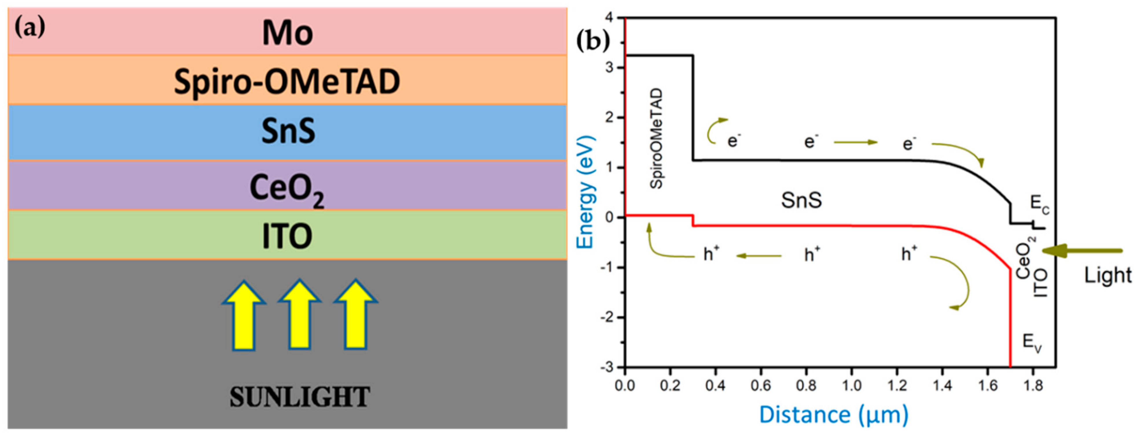
2. Structure and Material Properties of Solar Cell

The suggested ITO/CeO2/SnS/Spiro-OMeTAD/Mo solar cell schematic structure is shown in Figure 1a. ITO serves as a front contact TCO, CeO2 works as the window layer, Spiro-OMeTAD operates as the HTL, SnS acts as the absorber layer and Mo serves as the rear contact. The suggested structure’s energy band diagram (Figure 1b) reveals that the conduction band of the absorber layer SnS is less than that of the CeO2 ETL layer, and the conduction band offset (CBO) between SnS and CeO2 layer is very small. As a result, electrons can flow from SnS to ITO easily through CeO2. So, the electrons can flexibly move through CeO2 from SnS to ITO. In between the absorber layer SnS and the ETL layer CeO2, there is a valance band offset (VBO) which is extremely high. As a result, the holes at ETL layer CeO2 will be blocked. The valance band of Spiro-OMeTAD HTL is higher than that of absorber layer SnS as shown in Figure 1b, and the valence band offset between these two layers is substantially smaller. In addition, the CBO between HTL layer Spiro-OMeTAD and absorber layer SnS is quite large, preventing electrons from SnS from reaching the back electrode. Table 1 lists the physical parameters for the simulations of ITO/CeO2/SnS/Spiro-OMeTAD/Mo heterostructure solar cell [20], whereas Table 2 lists the physical parameters of defect density present in SnS.

3. Results and Discussion

3.1. CeO2/SnS Solar Cell Open-Circuit Voltage

In solar cell, VOC (open-circuit voltage) is determined by the dark current density. For thin-film solar cell, it can be computed as:
JO = qni2S/ND
where q denotes the charge, ND denotes ETL doped concentration, S denotes radiative recombination rate at the absorber/electrode interface and ni denotes absorber material’s inherent carrier density. Hence, the dark current at the absorber/electrode contact is proportional to the surface recombination rate. As an outcome, the metallization of the absorber surface is crucial for improving both VOC and the performance of the cell. Figure 2a,b display the J-V curve and QE curve with and without Spiro-OMeTAD, respectively. The cell without Spiro-OMeTAD has VOC of 0.8421 V, FF of 80.98%, Jsc of 31.83 mA/cm2 and PCE of 21.71% and with Spiro-OMeTAD VOC is 0.8878 V, FF is 85.61%, Jsc is 33.74 mA/cm2 and PCE is 25.65%. As a result, the Spiro-OMeTAD HTL enhances the (VOC) voltage level as well as the PCE of the proposed solar cell. Due to excessive band offset, the Spiro-OMeTAD HTL appropriate band alignment will extend high potential, increasing the VOC. Figure 2b illustrates the Spiro-OMeTAD HTL, magnifying the quantum efficiency of the solar cell.

3.2. Effect of Spiro-OMeTAD/SnS Layers Interface on Defect Density

The role of the Spiro-OMeTAD/SnS interface on the performance of the solar cell was analyzed. The defect density varied from 1010 to 1018 cm−2, and the findings demonstrate that the density of interface defect of Spiro-OMeTAD/SnS has no impact on the performance of the solar cell till 1016 cm−2. With a further increase in the defect density above 1016 cm−2, the performance of the solar cell reduces marginally which can be solved by increasing the thickness of SnS layer.

3.3. Interface Defect Density of CeO2/SnS Layers

The probability of defect at CeO2/SnS interface varied from 1010 to 1018 cm−2. This defect increases the recombination rate due to which a decrease in VOC is observed. Series resistance also increases due to which fill factor decreases. As a result, the high CeO2/SnS defect is to blame for higher series resistance. This reveals that the density of CeO2/SnS defects has a huge influence on solar cell performance. The structural imperfections of the two materials as well as metal cation passage through the absorbent layer during cell manufacturing cause interfacial defects [18].

3.4. Working Temperature and Back Contact Metal Work Function

The effect of WF (work function) on the performance of the cell is evaluated as shown in Figure 3a–d. As the WF rises, VOC, FF and PCE also increase, up to a particular value of WF. This specifies that with higher WF, the majority of carrier barrier height decreases. As a result, WF has a profound impact on the performance of the solar cell. To achieve high efficiency, a suitable metal contact is required.
If we increase the temperature of a semiconductor device, the velocity of the charge carrier increases and the band energy decreases. The reduction in band energy results in the reduction of the bandgap. At high temperatures, there will be a loss of power. As shown in Figure 4a–d, JSC is unaffected by working temperature, whereas VOC decreases as working temperature rises. Therefore, increasing working temperature lowers the solar cell efficiency.

3.5. Series Resistance and Shunt Resistance

The Rs and Rsh have a great influence on the performance of solar cells. It rises from the metal contacts of layers and solar cell. The functioning of the device was evaluated by altering the resistance from 2 to 25 cm2. Figure 5a–d illustrates that the VOC and JSC are unaffected by RS; however, the FF and PCE drop as Rs is increasing causes power dissipation.
Manufacturing flaws are the cause of Rsh. The shunt resistance was altered from 100 to 1000 cm2. VOC reduces when Rsh lowers because of the reduction of current to Rsh. As seen in Figure 6a–d, Rsh > 600 Ω cm2 has very little effect on PCE. As a result, low shunt resistance has a huge impact on the performance of the cell.

3.6. Layer Thicknesses and Carrier Concentration of SnS, CeO2 and Spiro-OMeTAD Layer Optimization

The performance of the cell was evaluated in terms of layer thickness and carrier concentration. Fill factor and efficiency of 85.61% and 25.65% are established at Spiro-OMeTAD and CeO2 thicknesses as well as carrier concentration of 100 nm and 10−21 cm−3 accordingly.
The reduction of photogenerated charge carrier recombination is indicated by VOC increasing slightly with Spiro-OMeTAD carrier concentration. At Spiro-OMeTAD thickness and carrier concentration of >100 nm and 1016 cm−3, FF and PCE were found to decrease with thickness but were unaffected by carrier concentration. Whereas, at Spiro-OMeTAD carrier concentration > 1016 cm−3, FF and PCE increase with carrier concentration but are unaffected by thickness.
In cases of CeO2-when the thickness increases, VOC drops but increases as the carrier concentration rises. By CeO2 thickness, FF is unaffected, although it rises in proportion to concentration of CeO2.
The primary influential criteria in designing solar cells are carrier concentration and absorber layer thickness. To achieve maximal device efficiency, both the functions must be maintained. To test the working of the cell, the concentration and thickness are tuned from 1011 to 1021 cm−3 and 200 to 2000 nm, respectively. At SnS thickness of 1400 nm and carrier concentration of 1016 cm−3, maximum PCE of 25.65% was recorded.
Table 3 shows a comparison of experimental and simulation results. Our results appear to be in satisfactory correlation with those previously reported. The distinctions between simulations and experiments are important to their methodology. There is a significant difference between experimental and simulation results because experiments are performed directly on the target machine, whereas software simulations are never performed in this manner. The experiments give confirmation of the object’s true behavior, with variable measurement errors, while simulated results provide insights based on similar theoretical models. As a result, the distinction is mostly between the real object and its theoretical and numerical descriptions, especially when other errors are greatly minimized.

4. Conclusions

Using the SCAPS-1D simulator, the performance of the proposed cell structure ITO/CeO2/SnS/Spiro-OMeTAD/Mo has been analyzed. To investigate the cell performance, distinct parameters of CeO2, Spiro-OMeTAD and SnS are optimized. The Spiro-OMeTAD made a considerable donation to the open-circuit voltage and efficiency. The higher carrier concentration of the CeO2 ETL was found to be beneficial to cell performance. The thickness of SnS appears to be a key component in determining cell performance. Due to their large impact on the resistance in series, CeO2/SnS density of interface defect and SnS defect density were optimized. The maximum recorded PCE with Spiro-OMeTAD HTL is 25.65% with JSC of 33.74% mA/cm2, VOC of 0.887 V and fill factor of 85.61%. Our result shows that SnS-based proposed device structure could prove to be an efficient device for low-cost and highly efficient thin-film solar cell in future work.

Author Contributions

Data curation: P.T., Y.A.-H., S., P.L., D.K.D., B.A. and A.U.; formal analysis: P.T., M.F.A.; Y.A.-H., V.S., S., P.L., D.K.D., A.U., H.A., S.B; methodology: S., P.T., Y.A.-H., P.L., D.K.D., B.A. and A.U.; project administration: Y.A.-H., D.K.D. and A.U.; supervision: Y.A.-H., D.K.D. and A.U.; writing—original draft, P.T., Y.A.-H., S., P.L., D.K.D., A.U. and S.B.; All authors have read and agreed to the published version of the manuscript.

Funding

The Deanship of Scientific Research (DSR) at King Abdulaziz University, Jeddah, Saudi Arabia has funded this project, under grant no. (FP-100-43).

Conflicts of Interest

The authors declare no conflict of interest.

References

  1. Andrade-Arvizu, J.A.; Courel-Piedrahita, M.; Vigil-Galán, O. SnS-based thin-film solar cells: Perspectives over the last 25 years. J. Mater. Sci. Mater. Electron. 2015, 26, 4541–4556. [Google Scholar] [CrossRef]
  2. Di Mare, S.; Menossi, D.; Salavei, A.; Artegiani, E.; Piccinelli, F.; Kumar, A.; Mariotto, G.; Romeo, A. SnS thin film solar cells: Perspectives and limitations. Coatings 2017, 7, 34. [Google Scholar] [CrossRef] [Green Version]
  3. Reddy, V.R.M.; Cho, H.; Gedi, S.; Reddy, K.R.; Kim, W.K.; Park, C. Effect of sulfurization temperature on the efficiency of SnS solar cells fabricated by sulfurization of sputtered tin precursor layers using effusion cell evaporation. J. Alloys Compd. 2019, 806, 410–417. [Google Scholar] [CrossRef]
  4. Sinsermsuksakul, P.; Sun, L.; Lee, S.W.; Park, H.H.; Kim, S.B.; Yang, C.; Gordon, R.G. Overcoming Efficiency Limitations of SnS-Based Solar Cells. Adv. Energy Mater. 2014, 4, 1400496. [Google Scholar] [CrossRef]
  5. Steinmann, V.; Jaramillo, R.; Hartman, K.; Chakraborty, R.; Brandt, R.E.; Poindexter, J.R.; Lee, Y.S.; Sun, L.; Polizzotti, A.; Park, H.H.; et al. 3.88% Efficient Tin Sulfide Solar Cells Using Congruent Thermal Evaporation. Adv. Mater. 2014, 26, 7488–7492. [Google Scholar] [CrossRef]
  6. Green, M.; Dunlop, E.; Hohl-Ebinger, J.; Yoshita, M.; Kopidakis, N.; Hao, X. Solar cell efficiency tables (version 57). Prog. Photovoltaics Res. Appl. 2020, 29, 3–15. [Google Scholar] [CrossRef]
  7. Garmim, T.; Benaissa, N.; Soussi, L.; Mghaiouini, R.; Bouabdalli, E.M.; El Ghaouti, C.; El Jouad, Z.; Louardi, A.; Hartiti, B.; Monkade, M. Effect of alternative buffer layers for SnS based solar cells: Numerical analysis using SCAPS-1D. Mater. Today Proc. 2022, in press. [Google Scholar] [CrossRef]
  8. Mavlonov, A.; Razykov, T.; Raziq, F.; Gan, J.; Chantana, J.; Kawano, Y.; Nishimura, T.; Wei, H.; Zakutayev, A.; Minemoto, T.; et al. A review of Sb2Se3 photovoltaic absorber materials and thin-film solar cells. Sol. Energy 2020, 201, 227–246. [Google Scholar] [CrossRef]
  9. Andrade-Arvizu, J.A.; García-Sánchez, M.; Courel-Piedrahita, M.; Pulgarín-Agudelo, F.; Santiago-Jaimes, E.; Valencia-Resendiz, E.; Arce-Plaza, A.; Vigil-Galán, O. Suited growth parameters inducing type of conductivity conversions on chemical spray pyrolysis synthesized SnS thin films. J. Anal. Appl. Pyrolysis 2016, 121, 347–359. [Google Scholar] [CrossRef]
  10. Banotra, A.; Padha, N. Facile growth of SnS and SnS0.40Se0.60 thin films as an absorber layer in the solar cell structure. Mater. Today Proc. 2019, 26, 3420–3425. [Google Scholar] [CrossRef]
  11. Banu, S.; Ahn, S.J.; Eo, Y.J.; Gwak, J.; Cho, A. Tin monosulfide (SnS) thin films grown by liquid-phase deposition. Sol. Energy 2017, 145, 33–41. [Google Scholar] [CrossRef]
  12. Jeganath, K.; Choudhari, N.J.; Pai, G.S.; Rao, A.; Raviprakash, Y. Role of substrate temperature on spray pyrolysed metastable π-SnS thin films. Mater. Sci. Semicond. Process. 2020, 113, 105050. [Google Scholar] [CrossRef]
  13. Patel, M.; Mukhopadhyay, I.; Ray, A. Molar optimization of spray pyrolyzed SnS thin films for photoelectrochemical applications. J. Alloys Compd. 2015, 619, 458–463. [Google Scholar] [CrossRef]
  14. Devika, M.; Reddy, N.K.; Ramesh, K.; Patolsky, F.; Gunasekhar, K. Weak rectifying behaviour of p-SnS/n-ITO heterojunctions. Solid-State Electron. 2009, 53, 630–634. [Google Scholar] [CrossRef]
  15. Hegde, S.S.; Ramesh, K. Advances in low-cost and nontoxic materials based solar cell devices. J. Phys. Conf. Ser. 2021, 2070, 012043. [Google Scholar] [CrossRef]
  16. Miyawaki, T.; Ichimura, M. Fabrication of ZnS thin films by an improved photochemical deposition method and application to ZnS/SnS heterojunction cells. Mater. Lett. 2007, 61, 4683–4686. [Google Scholar] [CrossRef]
  17. Xu, J.; Yang, Y. Study on the performances of SnS heterojunctions by numerical analysis. Energy Convers. Manag. 2014, 78, 260–265. [Google Scholar] [CrossRef]
  18. Debnath, S.; Islam, M.R.; Khan, M.S.R. Optical properties of CeO2 thin films. Bull. Mater. Sci. 2007, 30, 315–319. [Google Scholar] [CrossRef] [Green Version]
  19. Sinsermsuksakul, P.; Hartman, K.; Kim, S.B.; Heo, J.; Sun, L.; Park, H.H.; Chakraborty, R.; Buonassisi, T.; Gordon, R.G. Enhancing the efficiency of SnS solar cells via band-offset engineering with a zinc oxysulfide buffer layer. Appl. Phys. Lett. 2013, 102, 053901. [Google Scholar] [CrossRef]
  20. Kumar, S.G.; Rao, K.S.R.K. Physics and chemistry of CdTe/CdS thin film heterojunction photovoltaic devices: Fundamental and critical aspects. Energy Environ. Sci. 2014, 7, 45–102. [Google Scholar] [CrossRef]
  21. Ghodsi, F.E.; Tepehan, F.Z. Investigation on the optical and structural properties of spin-coated CeO2-TiO2 thin films. Phys. Status Solidi A Appl. Mater. Sci. 2006, 203, 526–533. [Google Scholar] [CrossRef]
  22. Lou, Q.; Li, H.; Huang, Q.; Shen, Z.; Li, F.; Du, Q.; Jin, M.; Chen, C. Multifunctional CNT: TiO2 additives in spiro-OMeTAD layer for highly efficient and stable perovskite solar cells. EcoMat 2021, 3, e12099. [Google Scholar] [CrossRef]
  23. Lee, J.-W.; Park, N.-G. Perovskite solar cells. RSC Energy Environ. Ser. 2014, 1, 242–257. [Google Scholar] [CrossRef]
  24. Tumen-Ulzii, G.; Matsushima, T.; Adachi, C. Mini-Review on Efficiency and Stability of Perovskite Solar Cells with Spiro-OMeTAD Hole Transport Layer: Recent Progress and Perspectives. Energy Fuels 2021, 35, 18915–18927. [Google Scholar] [CrossRef]
  25. Belarbi, F.; Rahal, W.; Rached, D.; Benghabrit, S.; Adnane, M. A comparative study of different buffer layers for CZTS solar cell using Scaps-1D simulation program. Optik 2020, 216, 164743. [Google Scholar] [CrossRef]
  26. Kumar, A.; Thakur, A.D. Analysis Of SnS2 Buffer Layer And SnS Back Surface Layer Based CZTS Solar Cells Using SCAPS. arXiv 2015, arXiv:1510.05092. [Google Scholar] [CrossRef]
  27. Benabbas, S.; Rouabah, Z.; Bouarissa, N.; Chelali, N. The role of back surface field SnS layer in improvement of efficiency of CdTe thin film solar cells. Optik 2016, 127, 6210–6217. [Google Scholar] [CrossRef]
  28. Kutwade, V.V.; Gattu, K.P.; Sonawane, M.E.; Tonpe, D.A.; Mishra, M.K.; Sharma, R. Contribution in PCE enhancement: Numerical designing and optimization of SnS thin flm solar cell. J. Nanopart. Res. 2021, 23, 146. [Google Scholar] [CrossRef]
  29. Ahmmed, S.; Aktar, A.; Hossain, J.; Ismail, A.B.M. Enhancing the open circuit voltage of the SnS based heterojunction solar cell using NiO HTL. Sol. Energy 2020, 207, 693–702. [Google Scholar] [CrossRef]
Figure 1. (a) Schematic layout of the proposed heterostructure solar cell and (b) the energy band diagram of the proposed heterostructure solar cell.
Nanomaterials 12 02506 g001
Figure 2. (a) J-V curve and (b) quantum efficiency of a proposed solar cell.
Nanomaterials 12 02506 g002
Figure 3. Effect on (a) JSC, (b), Voc (c) FF (d) and PCE with variation of work function (eV) of the proposed device.
Nanomaterials 12 02506 g003
Figure 4. Effect on (a) JSC, (b)VOC, (c) FF and (d) PCE with variation of temperature of the proposed device.
Nanomaterials 12 02506 g004
Figure 5. Effect on (a) JSC, (b) VOC, (c) FF and (d) PCE with variation of series resistance of the proposed device.
Nanomaterials 12 02506 g005
Figure 6. Effect on (a) JSC, (b) VOC, (c) FF and (d) PCE with variation of shunt resistance of the proposed device.
Nanomaterials 12 02506 g006
Table 1. Physical parameters of ITO/CeO2/SnS/Spiro-OMeTAD/Mo heterostructure solar cell.
ParametersITOCeO2SnSSpiro-OMeTAD
Thickness (nm)501001400100
Band gap (eV)3.63.51.313.2
Electron affinity (eV)4.54.64.22.1
Dielectric permittivity (relative)8.99133
CB effective density of states (cm−3)2.2 × 10181 × 10201.18 × 10182.5 × 1018
VB effective density of states (cm−3)1.8 × 10182 × 10214.76 × 10181.8 × 1019
Electron mobility (cm2/Vs)101001302 × 104
Hole mobility (cm2/Vs)10254.32 × 104
Shallow uniform donor density Nd (cm−3)1 × 10211 × 102100
Shallow uniform acceptor density Na (cm−3)0010151 × 1020
Electron thermal velocity (cm/s)1 × 1071 × 1071 × 1071 × 107
Hole thermal velocity (cm/s)1 × 1071 × 1071 × 1071 × 107
Defect density (cm−3)01 × 10141 × 1014
Radiative recombination coefficient (cm3/s)02.3 × 10−92.3 × 10−92.3 × 10⁻⁹
Table 2. Interface values are employed in the device simulation.
ParametersSpiro-OMeTAD/SnS InterfaceCeO2/SnS Interface
Defect typeNeutralNeutral
Capture cross-section electrons (cm2)1 × 10−191 × 10−19
Capture cross-section holes (cm2)1 × 10−191 × 10−19
Defect energy level EtAbove the highest EvAbove the highest Ev
Energy with respect to a reference (eV)0.060.06
Total density (cm−2)1 × 10101 × 1010
Table 3. Comparison of physical parameters of various simulated and experimentally studied device structures.
StructuresVOC
V
JSC
mA/cm2
FF
%
PCE
%
References
SnS/Zn(O,S)
(experimentally)
0.24419.4242.972.04[19]
SnS/SnO2/Zn(O,S):N/ZnO
(experimentally)
0.37220.2058.004.36[4]
CZTS/SnS2/ZnO
(simulated)
0.717826.9965.6712.73[25]
Mo/SnS/CZTS/SnS2/ZnO
(simulated)
0.992220.1371.3314.24[26]
ZnO/CdS/CdTe/SnS/Ni
(simulated)
0.84526.4684.5021.83[27]
p-SnS/CdS/n-Zn MgO
(simulated)
~0.738.5483~23[28]
ITO/CeO2/SnS/NiO/Mo
(simulated)
0.89032.6786.1925.06[29]
ITO/CeO2/SnS/Spiro-OMeTAD
(simulated)
0.88733.7485.6125.65This paper
Publisher’s Note: MDPI stays neutral with regard to jurisdictional claims in published maps and institutional affiliations.

