
All-Dielectric Transreflective Angle-Insensitive Near-Infrared (NIR) Filter


Abstract
:1. Introduction
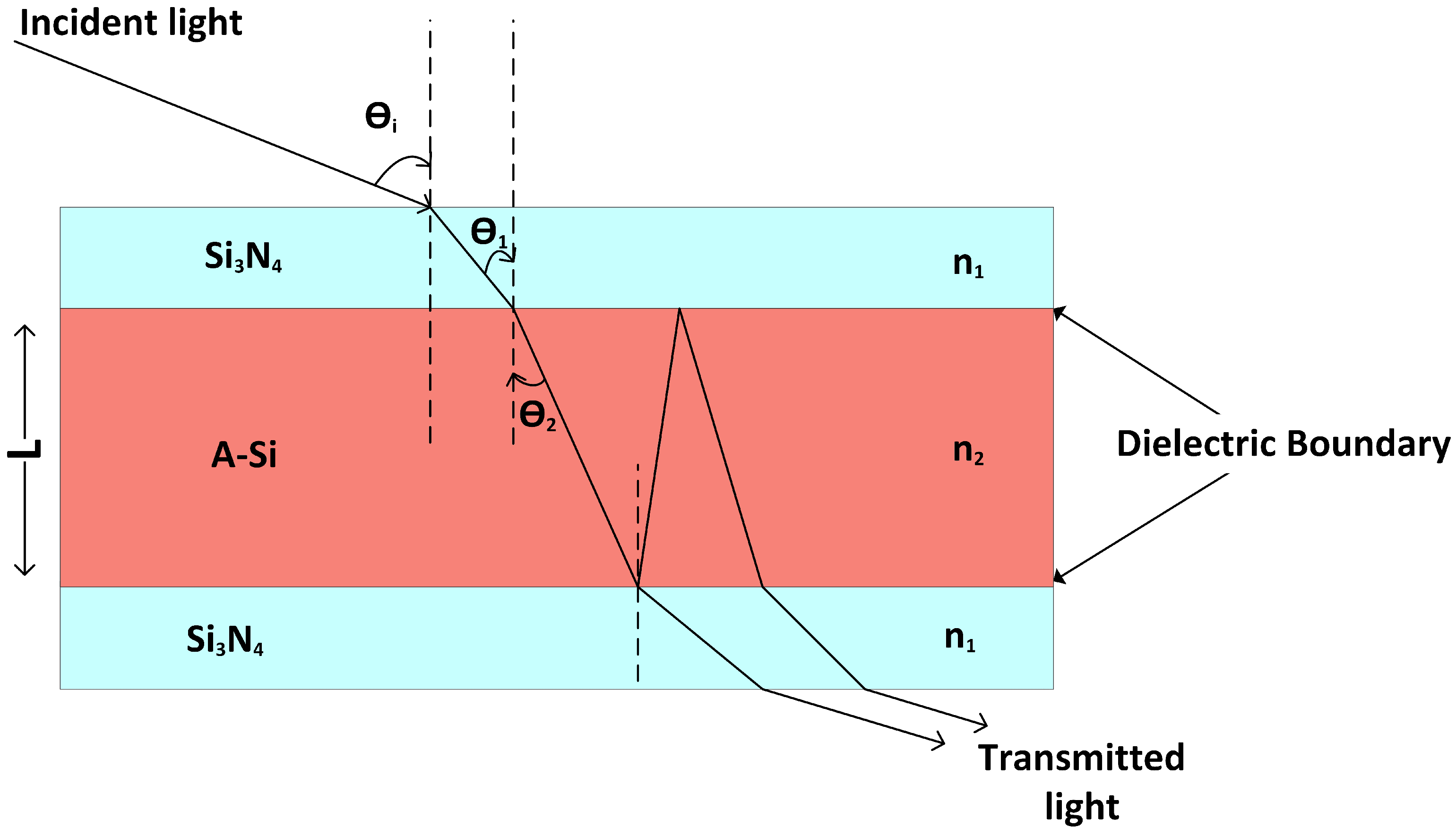
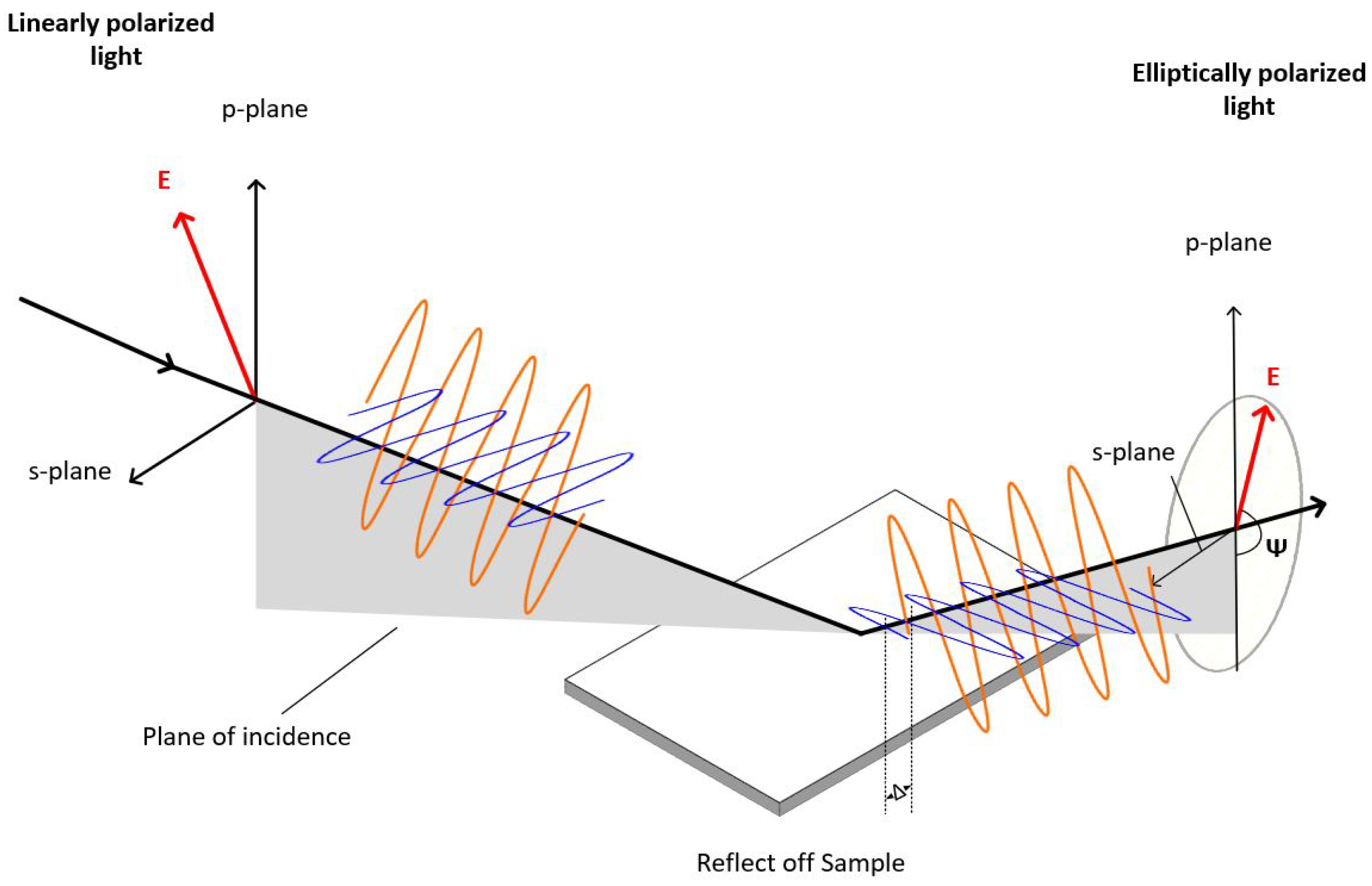
2. Design Methodology
3. Results and Discussion
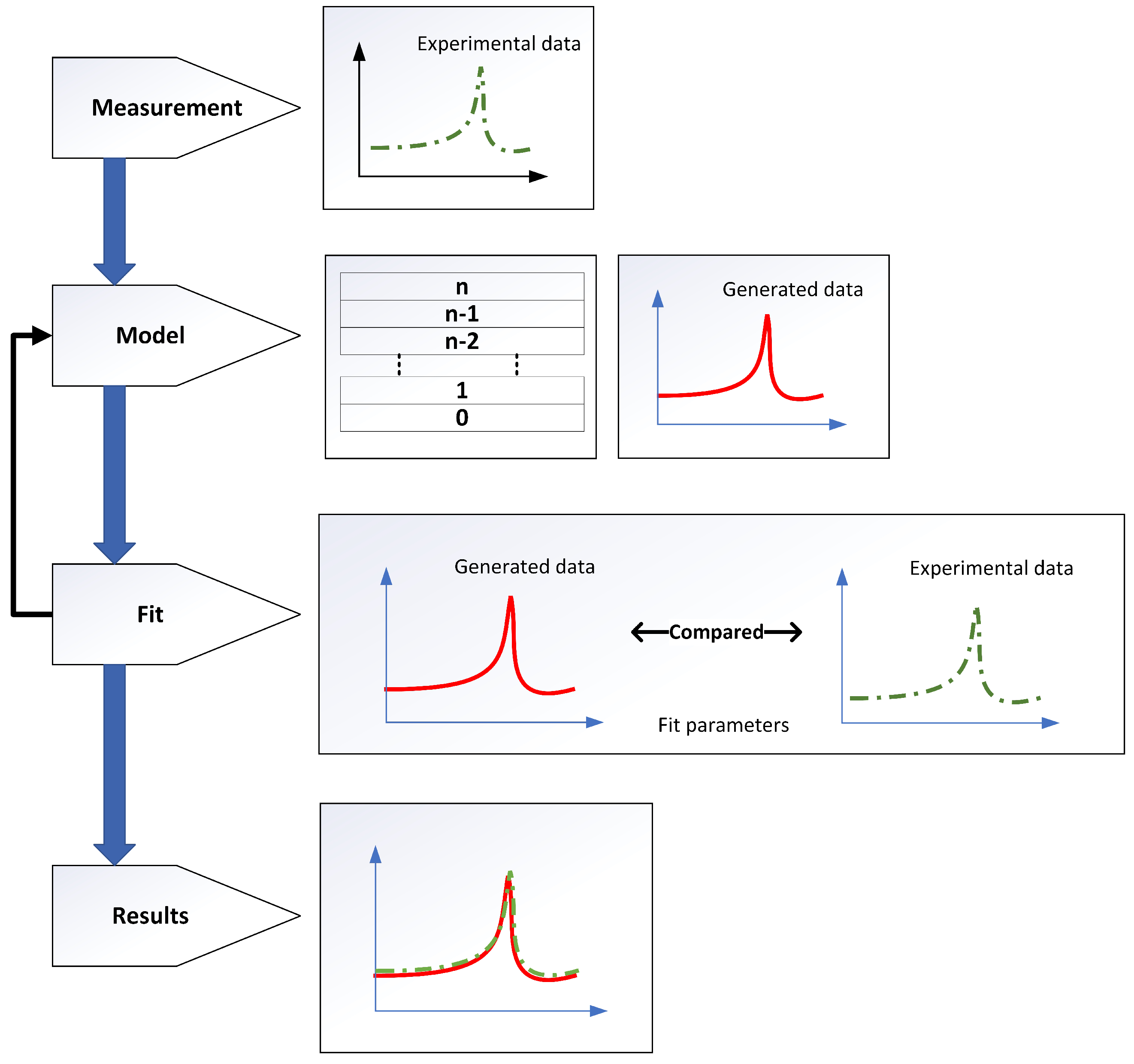
- The first step is to acquire the experimental data of the sample. In this particular case, a Perkin Elmer Lambda 1050 UV-Vis-NIR spectrophotometer was used to collect the transmission and reflection experimental data.
- The second step is to create an accurate optical model of the sample system. Here, every material in the system, such as the substrate and the A-Si and SiN layers, was viewed as a “layer”. This model was used to generate SE data.
- In the third step, the model fit parameters (such as n&k values of each layer, thickness etc.) are defined, and the software adjusts them automatically to improve the agreement between measured and model-generated SE data. This is referred to as “fitting” the data.
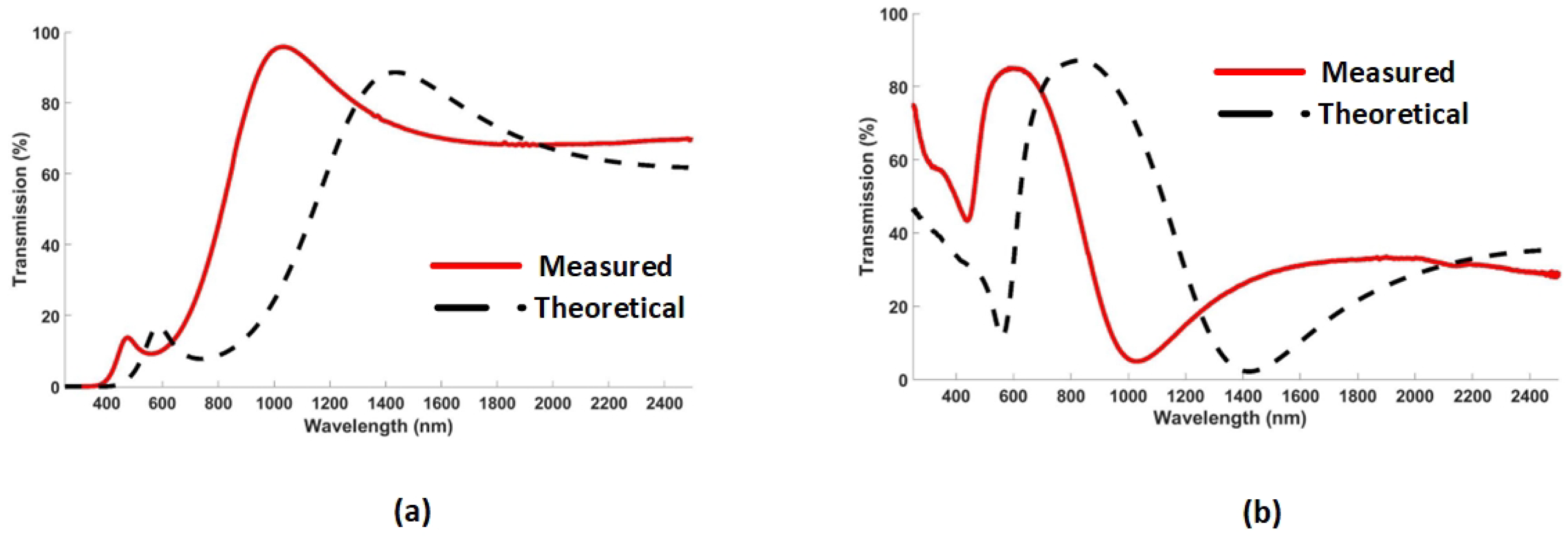
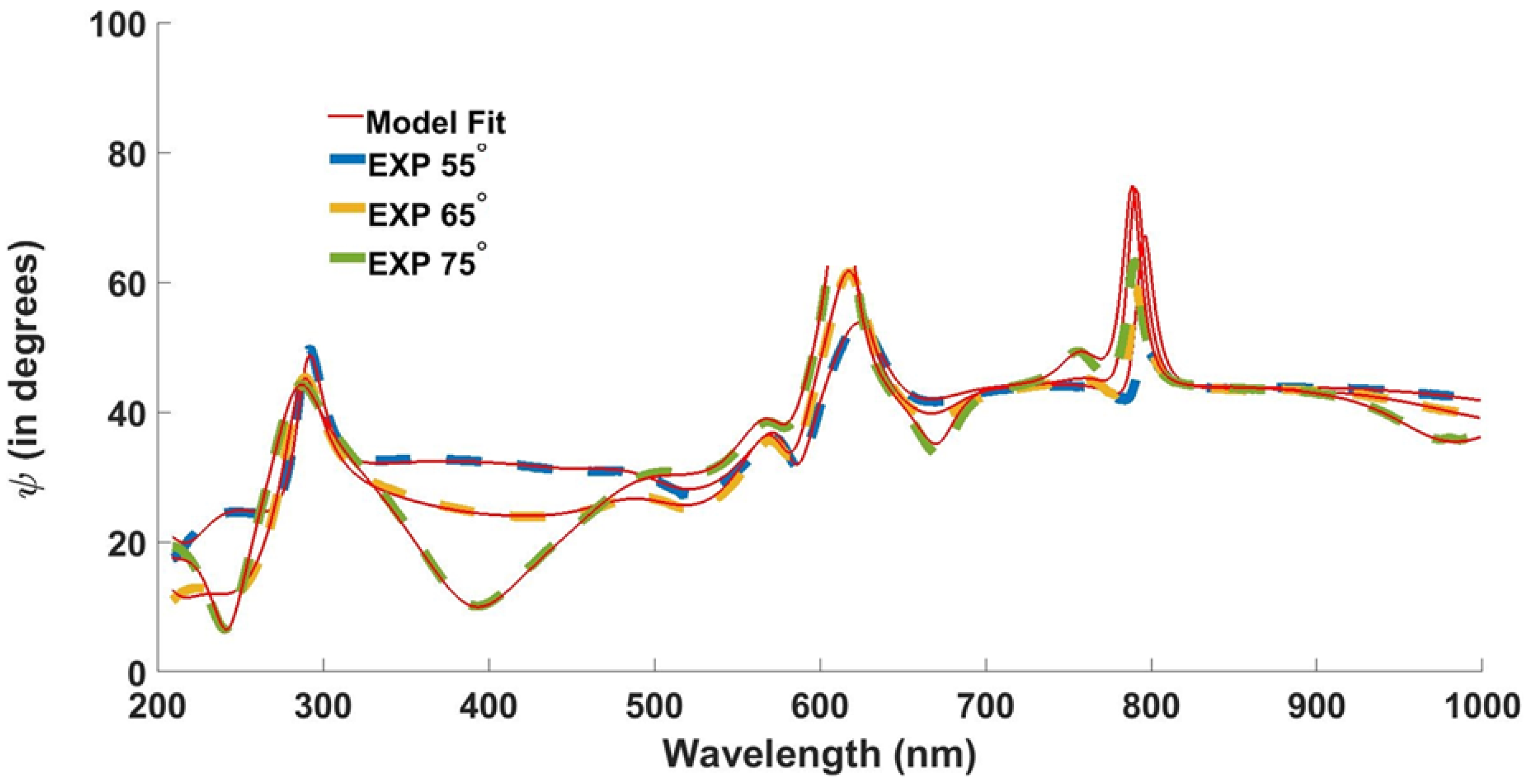
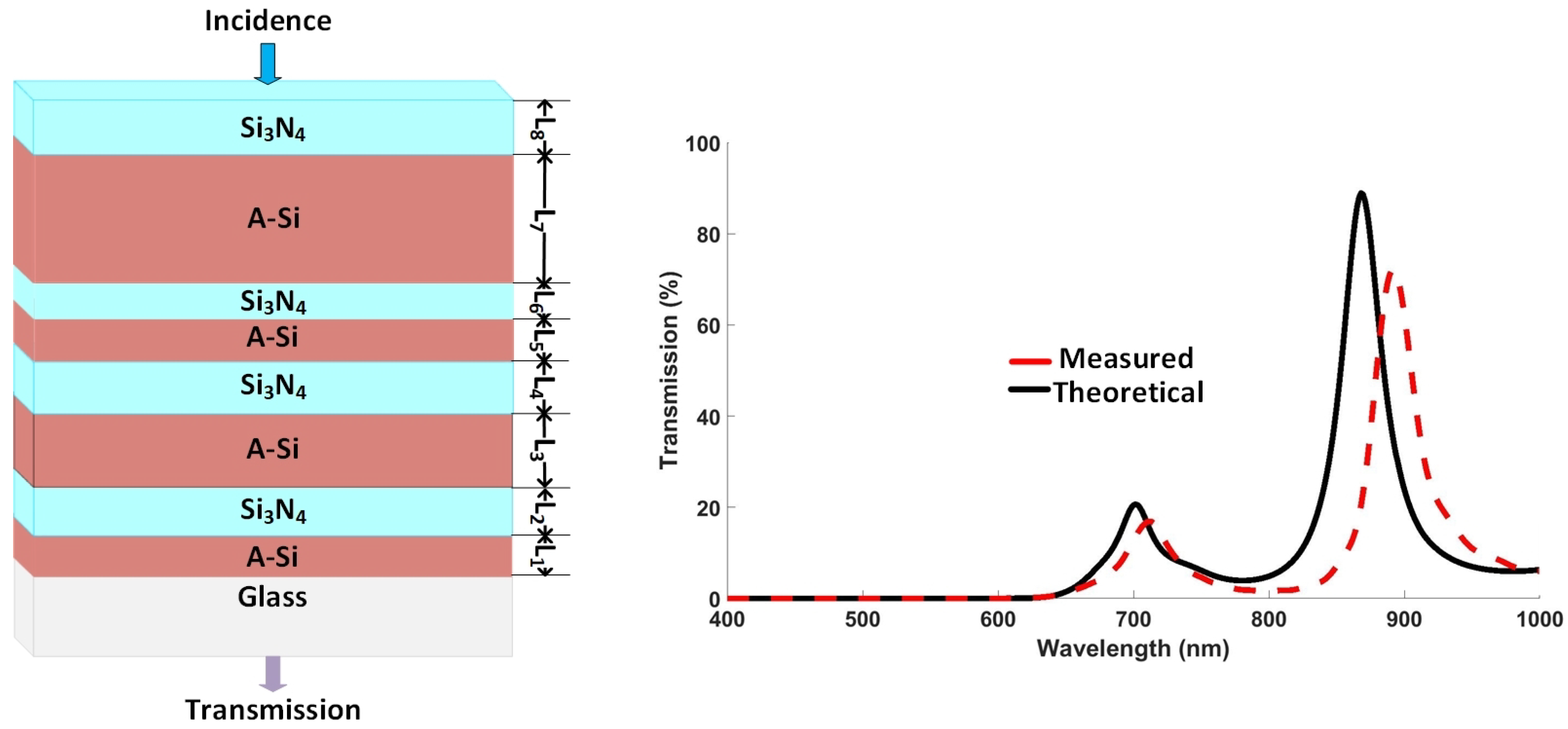
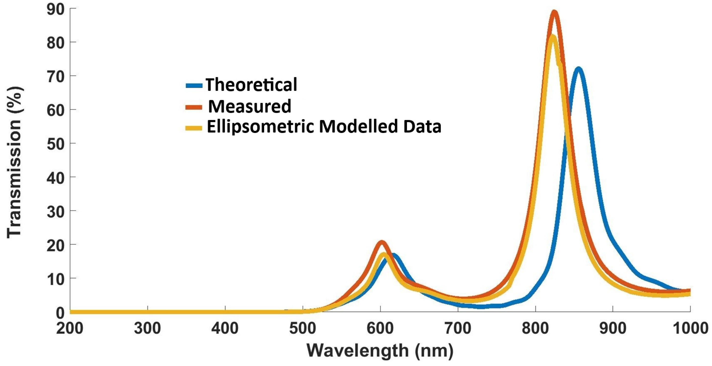
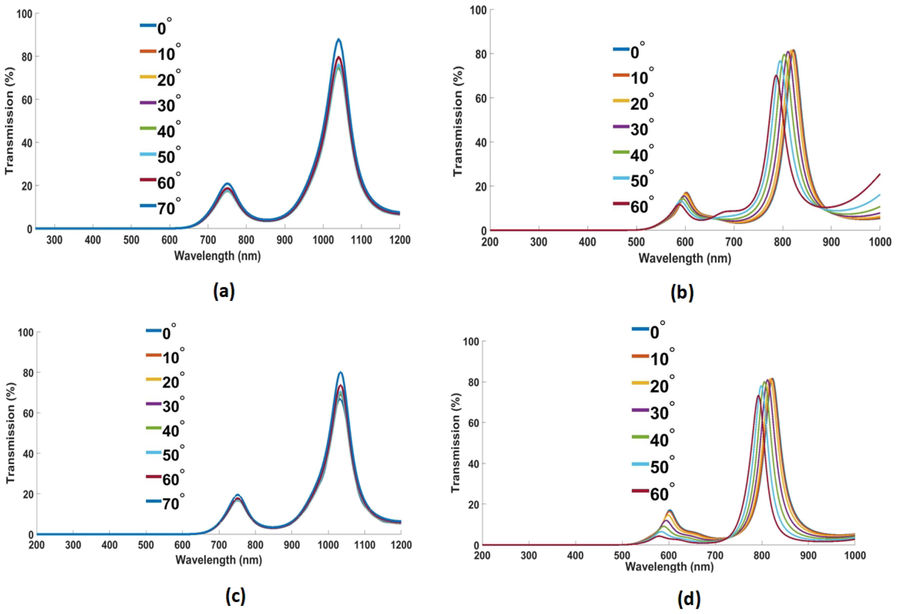
- The fit’s outcomes are assessed. If the results are not satisfactory, the optical model and/or fit parameters are modified, and the data is re-fitted. Mean-squared error (MSE) is a parameter that evaluates the quality of the match between the generated and the experimental data [43]. Mathematically, it is given aswhere N is the number of pairs, M is the number of variable parameters in the model, and is the standard deviation on the experimental data points. MSE should be positive and near-zero for the maximum likelihood estimate. Figure 8 shows the model fitted to the experimental data with mean-squared error (MSE) = 30.51, when the light is incident at , , and angles.
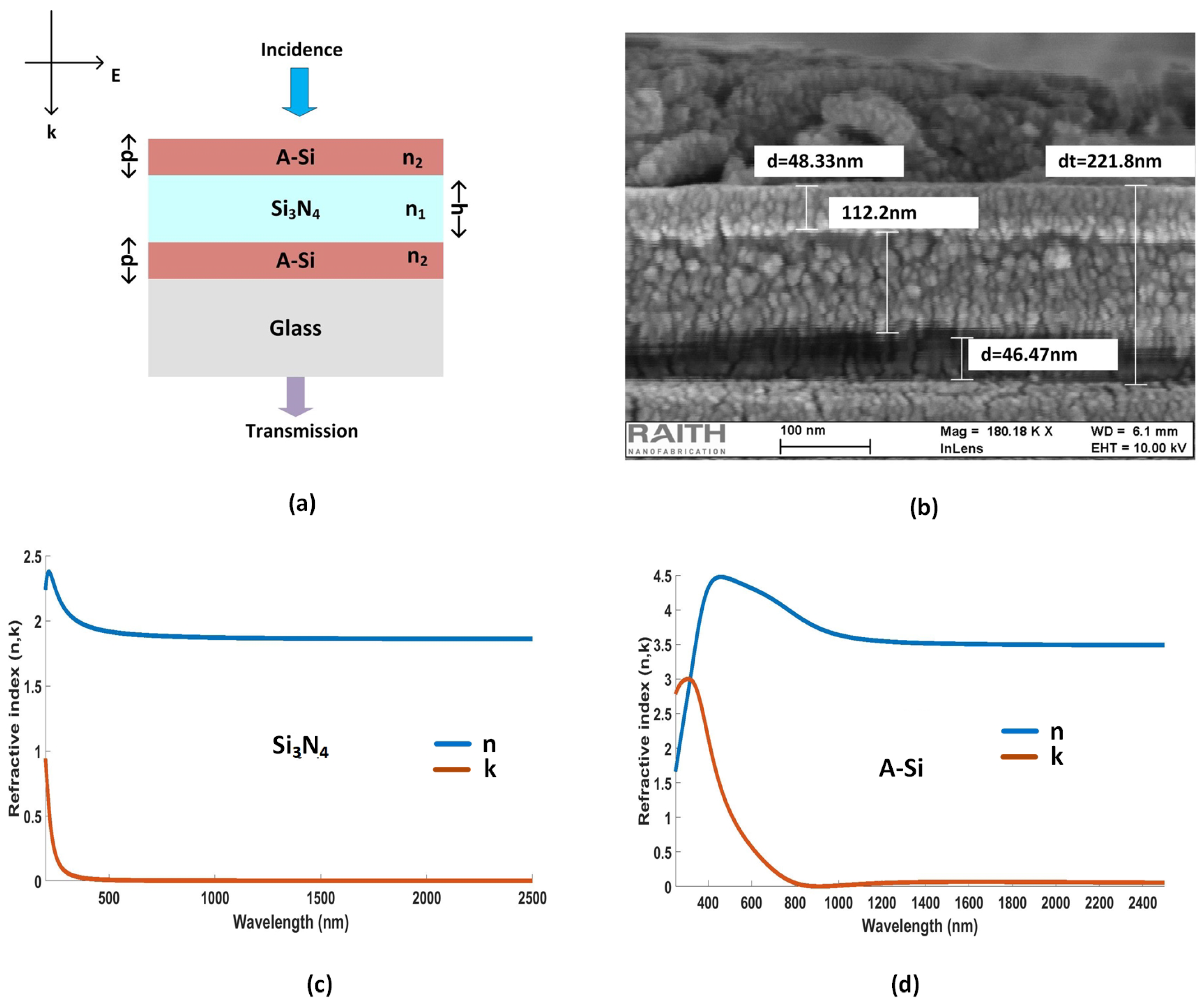
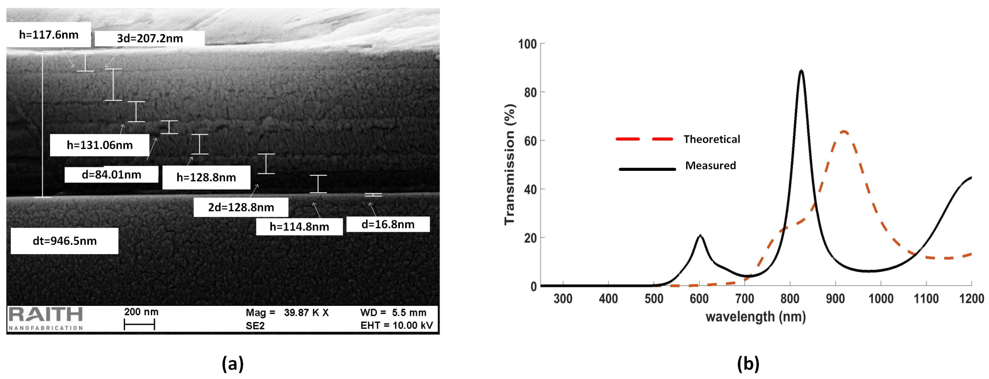
3.1. Fabrication
3.2. Film Characterization
4. Conclusions
Author Contributions
Funding
Data Availability Statement
Acknowledgments
Conflicts of Interest
Abbreviations
| ANFF | Australian National Fabrication Facility |
| CMOS | complementary metal-oxide semiconductor |
| EBL | electron beam lithography |
| FOM | figure of merit |
| GMR | guided mode resonance |
| MSE | mean-squared error |
| NIR | near infrared |
| PECVD | plasma-enhanced chemical vapor deposition |
| PML | perfectly matched layers |
| SE | spectroscopic ellipsometry |
| SEM | scanning electron microscopy |
| TE | transverse electric |
| TM | transverse magnetic |
| WVASE | Woollam variable-angle spectroscopic ellipsometry |
References
- ElMasry, G.; ElGamal, R.; Mandour, N.; Gou, P.; Al-Rejaie, S.; Belin, E.; Rousseau, D. Emerging thermal imaging techniques for seed quality evaluation: Principles and applications. Food Res. Int. 2020, 131, 109025. [Google Scholar] [CrossRef] [PubMed]
- Liu, J. Smoothing filter-based intensity modulation: A spectral preserve image fusion technique for improving spatial details. Int. J. Remote Sens. 2000, 21, 3461–3472. [Google Scholar] [CrossRef]
- Hook, S.J.; Johnson, W.R.; Abrams, M.J. NASA’s hyperspectral thermal emission spectrometer (HyTES). In Thermal Infrared Remote Sensing; Springer: Berlin/Heidelberg, Germany, 2013; pp. 93–115. [Google Scholar]
- Zheng, Z.; Luo, Y.; Yang, H.; Yi, Z.; Zhang, J.; Song, Q.; Yang, W.; Liu, C.; Wu, X.; Wu, P. Thermal tuning of terahertz metamaterial absorber properties based on VO2. Phys. Chem. Chem. Phys. 2022, 24, 8846–8853. [Google Scholar] [CrossRef] [PubMed]
- Modir, N.; Shahedi, M.; Dormer, J.; Fei, B. Development of a real-time spectral imaging system using in-site LED-based illumination for endoscopic applications. In High-Speed Biomedical Imaging and Spectroscopy VI; SPIE: Bellingham, WA, USA.
- Sousa, E.; Vardasca, R.; Teixeira, S.; Seixas, A.; Mendes, J.; Costa-Ferreira, A. A review on the application of medical infrared thermal imaging in hands. Infrared Phys. Technol. 2017, 85, 315–323. [Google Scholar] [CrossRef]
- Bitas, D.; Papastavros, K.; Tsipianitis, D. A Smart Cablebot for Spectral Imaging and Micro-climate measurements inside Greenhouses. In Proceedings of the 2020 11th International Conference on Information, Intelligence, Systems and Applications (IISA), Piraeus, Greece, 15–17 July 2020; pp. 1–4. [Google Scholar]
- Xiang, H.; Tian, L. Development of a low-cost agricultural remote sensing system based on an autonomous unmanned aerial vehicle (UAV). Biosyst. Eng. 2011, 108, 174–190. [Google Scholar] [CrossRef]
- Yuen, P.W.; Richardson, M. An introduction to hyperspectral imaging and its application for security, surveillance and target acquisition. Imaging Sci. J. 2010, 58, 241–253. [Google Scholar] [CrossRef]
- Koz, A. Ground-Based Hyperspectral Image Surveillance Systems for Explosive Detection: Part I—State of the Art and Challenges. IEEE J. Sel. Top. Appl. Earth Obs. Remote Sens. 2019, 12, 4746–4753. [Google Scholar] [CrossRef]
- Chen, H.; Chen, Z.; Yang, H.; Wen, L.; Yi, Z.; Zhou, Z.; Dai, B.; Zhang, J.; Wu, X.; Wu, P. Multi-mode surface plasmon resonance absorber based on dart-type single-layer graphene. RSC Adv. 2022, 12, 7821–7829. [Google Scholar] [CrossRef]
- Deng, Y.; Cao, G.; Yang, H.; Zhou, X.; Wu, Y. Dynamic control of double plasmon-induced transparencies in aperture-coupled waveguide-cavity system. Plasmonics 2018, 13, 345–352. [Google Scholar] [CrossRef]
- Liu, J.N.; Schulmerich, M.V.; Bhargava, R.; Cunningham, B.T. Optimally designed narrowband guided-mode resonance reflectance filters for mid-infrared spectroscopy. Opt. Express 2011, 19, 24182–24197. [Google Scholar] [CrossRef] [Green Version]
- Nguyen, D.T.; Ababtain, M.; Memon, I.; Ullah, A.; Istock, A.; Woidt, C.; Xie, W.; Lehmann, P.; Hillmer, H. 3D nanoimprint for NIR Fabry-Pérot filter arrays: Fabrication, characterization and comparison of different cavity designs. Appl. Nanosci. 2016, 6, 1127–1135. [Google Scholar] [CrossRef] [Green Version]
- Nguyen, D.M.; Lee, D.; Rho, J. Control of light absorbance using plasmonic grating based perfect absorber at visible and near-infrared wavelengths. Sci. Rep. 2017, 7, 2611. [Google Scholar] [CrossRef] [PubMed] [Green Version]
- Shaukat, A.; Noble, F.; Arif, K.M. Nanostructured Color Filters: A Review of Recent Developments. Nanomaterials 2020, 10, 1554. [Google Scholar] [CrossRef]
- Kodali, A.K.; Schulmerich, M.; Ip, J.; Yen, G.; Cunningham, B.T.; Bhargava, R. Narrowband midinfrared reflectance filters using guided mode resonance. Anal. Chem. 2010, 82, 5697–5706. [Google Scholar] [CrossRef] [Green Version]
- Shah, Y.D.; Grant, J.; Hao, D.; Kenney, M.; Pusino, V.; Cumming, D.R.S. Ultra-narrow Line Width Polarization-Insensitive Filter Using a Symmetry-Breaking Selective Plasmonic Metasurface. ACS Photonics 2018, 5, 663–669. [Google Scholar] [CrossRef] [Green Version]
- Fano, U. The theory of anomalous diffraction gratings and of quasi-stationary waves on metallic surfaces (Sommerfeld’s waves). JOSA 1941, 31, 213–222. [Google Scholar] [CrossRef]
- Wang, M. Lithography; BoD–Books on Demand: Norderstedt, Germany, 2010. [Google Scholar]
- Chen, J.; Nie, H.; Tang, C.; Cui, Y.; Yan, B.; Zhang, Z.; Kong, Y.; Xu, Z.; Cai, P. Highly sensitive refractive-index sensor based on strong magnetic resonance in metamaterials. Appl. Phys. Express 2019, 12, 052015. [Google Scholar] [CrossRef]
- Ng, R.C.; Garcia, J.C.; Greer, J.R.; Fountaine, K.T. Polarization-Independent, Narrowband, Near-IR Spectral Filters via Guided Mode Resonances in Ultrathin a-Si Nanopillar Arrays. ACS Photonics 2019, 6, 265–271. [Google Scholar] [CrossRef]
- Chhowalla, M.; Teo, K.; Ducati, C.; Rupesinghe, N.; Amaratunga, G.; Ferrari, A.; Roy, D.; Robertson, J.; Milne, W. Growth process conditions of vertically aligned carbon nanotubes using plasma enhanced chemical vapor deposition. J. Appl. Phys. 2001, 90, 5308–5317. [Google Scholar] [CrossRef]
- Ng, R.C.; Garcia, J.C.; Greer, J.R.; Fountaine, K.T. Miniaturization of a-Si guided mode resonance filter arrays for near-IR multi-spectral filtering. Appl. Phys. Lett. 2020, 117, 111106. [Google Scholar] [CrossRef]
- Grepstad, J.O.; Greve, M.M.; Holst, B.; Johansen, I.R.; Solgaard, O.; Sudbø, A. Finite-size limitations on quality factor of guided resonance modes in 2D photonic crystals. Opt. Express 2013, 21, 23640–23654. [Google Scholar] [CrossRef] [PubMed] [Green Version]
- Im, C.S.; Lee, S.S. Highly efficient and angle-tolerant mid-infrared filter based on a cascaded etalon resonator. Opt. Express 2017, 25, 16083–16091. [Google Scholar] [CrossRef] [PubMed]
- Shrestha, V.R.; Lee, S.S.; Kim, E.S.; Choi, D.Y. Non-iridescent transmissive structural color filter featuring highly efficient transmission and high excitation purity. Sci. Rep. 2014, 4, 4921. [Google Scholar] [CrossRef] [PubMed] [Green Version]
- Noh, T.H.; Yoon, Y.T.; Lee, H.S.; Lee, S.; Choi, D. Highly angle tolerant filter incorporating serially cascaded a-Si based etalons and its application to a compact receiver. Opt. Express 2013, 21 1, 1301–1309. [Google Scholar] [CrossRef]
- Lee, H.S.; Hwang, G.W.; Seong, T.Y.; Park, J.; Kim, J.W.; Kim, W.M.; Kim, I.; Lee, K.S. Design of mid-infrared filter array based on plasmonic metal nanodiscs array and its application to on-chip spectrometer. Sci. Rep. 2021, 11, 12218. [Google Scholar] [CrossRef]
- Ji, C.; Yang, C.; Shen, W.; Lee, K.T.; Zhang, Y.; Liu, X.; Guo, L.J. Decorative near-infrared transmission filters featuring high-efficiency and angular-insensitivity employing 1D photonic crystals. Nano Res. 2019, 12, 543–548. [Google Scholar] [CrossRef]
- Ding, F.; Dai, J.; Chen, Y.; Zhu, J.; Jin, Y.; Bozhevolnyi, S.I. Broadband near-infrared metamaterial absorbers utilizing highly lossy metals. Sci. Rep. 2016, 6, 39445. [Google Scholar] [CrossRef] [Green Version]
- Liu, N.; Mesch, M.; Weiss, T.; Hentschel, M.; Giessen, H. Infrared Perfect Absorber and Its Application As Plasmonic Sensor. Nano Lett. 2010, 10, 2342–2348. [Google Scholar] [CrossRef]
- Miyamichi, A.; Ono, A.; Kamehama, H.; Kagawa, K.; Yasutomi, K.; Kawahito, S. Multi-band plasmonic color filters for visible-to-near-infrared image sensors. Opt. Express 2018, 26, 25178–25187. [Google Scholar] [CrossRef]
- Jang, W.Y.; Ku, Z.; Jeon, J.; Kim, J.O.; Lee, S.J.; Park, J.; Noyola, M.J.; Urbas, A. Experimental demonstration of adaptive infrared multispectral imaging using plasmonic filter array. Sci. Rep. 2016, 6, 1–9. [Google Scholar] [CrossRef]
- Born, M.E. Wolf Principles of optics. Pergamon Press 1980, 6, 36–111. [Google Scholar]
- Yang, C.; Shen, W.; Zhang, Y.; Li, K.; Fang, X.; Zhang, X.; Liu, X. Compact multilayer film structure for angle insensitive color filtering. Sci. Rep. 2015, 5, 9285. [Google Scholar] [CrossRef] [PubMed]
- Lee, K.; Seo, S.; Lee, J.Y.; Guo, L.J. Strong Resonance Effect in a Lossy Medium-Based Optical Cavity for Angle Robust Spectrum Filters. Adv. Mater. 2014, 26, 6324–6328. [Google Scholar] [CrossRef]
- Li, Z.; Palacios, E.; Butun, S.; Kocer, H.; Aydin, K. Omnidirectional, broadband light absorption using large-area, ultrathin lossy metallic film coatings. Sci. Rep. 2015, 5, 15137. [Google Scholar] [CrossRef] [PubMed]
- Deng, Y.; Cao, G.; Wu, Y.; Zhou, X.; Liao, W. Theoretical description of dynamic transmission characteristics in MDM waveguide aperture-side-coupled with ring cavity. Plasmonics 2015, 10, 1537–1543. [Google Scholar] [CrossRef]
- Fujiwara, H. Spectroscopic Ellipsometry: Principles and Applications; John Wiley & Sons: Hoboken, NJ, USA, 2007. [Google Scholar]
- Woollam, J.A.; Hilfiker, J.N.; Bungay, C.L.; Synowicki, R.A.; Tiwald, T.E.; Thompson, D.W. Spectroscopic ellipsometry from the vacuum ultraviolet to the far infrared. In AIP Conference Proceedings; American Institute of Physics: College Park, MD, USA, 2001; Volume 550, pp. 511–518. [Google Scholar]
- Tompkins, H.; Irene, E.A. Handbook of Ellipsometry; William Andrew: Amsterdam, The Netherlands, 2005. [Google Scholar]
- Moré, J.J. The Levenberg–Marquardt algorithm: Implementation and theory. In Numerical Analysis; Springer: Berlin/Heidelberg, Germany, 1978; pp. 105–116. [Google Scholar]


| Ref. | Design | Fabrication Technique |
|---|---|---|
| [22] | GMR-based 2D A-Si nanodisk array embedded in SiO. | EBL and PECVD. |
| [31] | Ti nanodisk-shaped array with Ti/Au/SiO. | E-beam evaporation and RF sputtering. |
| [32] | MgF nanodisk-shaped array with MgF/Au/SiO. | E-beam evaporation and EBL. |
| [33] | A single aperture surrounded by concentric periodic corrugations on a silver (Ag) thin film for simultaneous imaging of a spectral range from the visible to the near-infrared | EBL, vacuum evaporation, and an FIB. |
| [29] | Triangular lattice of Al nanodisks with Al/SiO. | NIL and subsequent lift-off process. |
| [18] | Symmetry-breaking elliptical nanoholed Au sheet on SiO, with FWHM of 79 nm and efficiency up to 44%. | EBL and annealing. |
| [34] | Au circular nanohole sheet on a GaAs substrate for infrared filtering. | EBL and e-beam evaporation. |
| [17] | GMR-based 1D SiN grating on soda lime substrate for infrared filtration. | Contact photolithography and PECVD. |
| [26] | Hybrid cascaded multilayered thin-film filter Si/SiO, for mid-infra-red filtration. | E-beam and resistance-heating methods. |
| [28] | Cascaded thin-film filter (A-Si/SiO), provided sharp roll-off, and 130 nm bandwidth. | PECVD |
| [27] | Cascaded thin-film filter (A-Si/SiO), investigated to filter the red color (620–750 nm). | PECVD |
| [30] | Multilayered thin-film filter (A-Si/SiN) studied for blocking the visible region (400–700 nm). | PECVD |
| [This work] | Hybrid, cascaded, thin-film filter (A-Si/SiN) for NIR filtering with an FWHM of 77 nm. | PECVD |
| Layer Numbers | Symbol | Material | Thicknesses (nm) |
|---|---|---|---|
| 1 | L | A-Si | 54.730 |
| 2 | L | SiN | 84.430 |
| 3 | L | A-Si | 112.557 |
| 4 | L | SiN | 112.043 |
| 5 | L | A-Si | 52.043 |
| 6 | L | SiN | 106.518 |
| 7 | L | A-Si | 165.611 |
| 8 | L | SiN | 101.408 |
Publisher’s Note: MDPI stays neutral with regard to jurisdictional claims in published maps and institutional affiliations. |
© 2022 by the authors. Licensee MDPI, Basel, Switzerland. This article is an open access article distributed under the terms and conditions of the Creative Commons Attribution (CC BY) license (https://creativecommons.org/licenses/by/4.0/).
Share and Cite
Shaukat, A.; Umer, R.; Noble, F.; Arif, K.M. All-Dielectric Transreflective Angle-Insensitive Near-Infrared (NIR) Filter. Nanomaterials 2022, 12, 2537. https://doi.org/10.3390/nano12152537
Shaukat A, Umer R, Noble F, Arif KM. All-Dielectric Transreflective Angle-Insensitive Near-Infrared (NIR) Filter. Nanomaterials. 2022; 12(15):2537. https://doi.org/10.3390/nano12152537
Chicago/Turabian StyleShaukat, Ayesha, Rahila Umer, Frazer Noble, and Khalid Mahmood Arif. 2022. "All-Dielectric Transreflective Angle-Insensitive Near-Infrared (NIR) Filter" Nanomaterials 12, no. 15: 2537. https://doi.org/10.3390/nano12152537