Article

Spectrally Stable Blue Light-Emitting Diodes Based on All-Inorganic Halide Perovskite Films

1
State Key Laboratory of Luminescence and Applications, Changchun Institute of Optics, Fine Mechanics and Physics, Chinese Academy of Sciences, Dong_Nanhu Road 3888, Changchun 130033, China
2
University of Chinese Academy of Sciences, Beijing 100049, China
3
Changchun University of Chinese Medicine, Changchun 130017, China
4
School of Optoelectronic Engineering and Instrumentation Science, Dalian University of Technology, Dalian 116024, China
5
Key Lab of Physics and Technology for Advanced Batteries (Ministry of Education), Department of Physics, Jilin University, Changchun 130012, China
*
Authors to whom correspondence should be addressed.
Nanomaterials 2022, 12(17), 2906; https://doi.org/10.3390/nano12172906
Submission received: 29 June 2022 / Revised: 6 August 2022 / Accepted: 11 August 2022 / Published: 24 August 2022

Abstract

:
Substantial progress has been made in perovskite light-emitting diodes (PeLEDs), but the fabrication of high-performance blue PeLEDs still remains a challenge due to its low efficiency, spectral instability and short operational lifetime. How to produce an efficient and stable blue PeLED is the key to realizing the application of PeLEDs in full-color displays. We herein report a blue PeLED usint the ligand-assisted reprecipitation method, in which phenylethylammonium bromide (PEABr) was used as ligands, and chloroform was used as anti-solvent to prepare blue perovskite nanocrystal films. By increasing the PEABr content from 40% to 100% (The ratio of x% PEABr refers to the molar ratio between PEABr and PbBr2), the film quality is highly improved, and the emission exhibits a blue shift. Introducing a poly(9-vinylcarbazole) (PVK) hole transport layer into the device, the PVK layer can not only achieve efficient hole injection, but can also isolate the PEDOT: PSS layer to inhibit the non-radiative recombination of metal halide luminescence layer, reduce surface ion defects and successfully inhibit halide atom migration. Finally, the PeLED presents a stable electroluminescence under different driving voltages without any red shift.

1. Introduction

In recent years, all-inorganic metal halide perovskite materials have been widely used in the lighting and display fields due to their high color purity, easy band gap adjustment, narrow-band emission and high fluorescence quantum efficiency, making them ideal candidate materials for the preparation of next-generation light-emitting diodes (LEDs) [1,2,3,4,5,6,7]. As researchers have optimized perovskite composition [8], film quality [9], and device structure [10], great breakthroughs have been made in the external quantum efficiency (EQE) of perovskite light-emitting diodes (PeLEDs) during the past few years. The highest EQE of near-infrared, red and green PeLEDs has exceeded 20% [8,10,11,12,13,14], which is comparable to other commercial quantum-dot and organic LEDs.
As one of the three primary colors of white light, the blue PeLEDs still perform poorly compared with green and red PeLEDs [15,16,17,18], which is due to the fact that the chloride-doped blue PeLEDs are very sensitive to power supply and voltage fluctuations. In other words, the power supply will inevitably suffer voltage fluctuations, which will lead to peak wavelength shift, decreased light efficiency and the inferior reliability of blue PeLEDs [16,19]. This seriously affects its color purity and hinders the commercialization of blue PeLED. Therefore, we still need more effective methods to improve the spectral stability of the devices for chloride-doped perovskite, especially in the applications where the wavelength accuracy and luminous stability of LED are strictly required. Therefore, the blue PeLED need a more stable perovskite emission layer when they are operated in a higher working voltage or a stronger electric field. Therefore, how to improve its EQE and spectralstability is an essential step to accelerate the applications of blue devices.
In general, the realization of blue perovskite luminescence is mainly through halogen-doping component engineering and dimension regulation based on the quantum confining effect. The former tunes the bandgap of the mixed halide perovskite by controlling the bromine and chlorine doping components to realize the emission of blue light from perovskite [20,21,22,23]. The latter is a quasi-two-dimensional perovskite or quantum dot that can form a three-dimensional perovskite cambium by adding an organic ammonium salt or other ligands with long chains [24,25,26]. Yao et al. successfully obtained the blue emission of CsPbBrxCl3−x nanoparticles at 470 nm through halogen-doping component engineering [27]. However, a large amount of Cl- vacancies were easily formed due to the doping of a large amount of chlorine, which introduced deep-level defects, leading to strong non-radiative recombination, hence reducing the luminous efficiency of the blue light PeLEDs [28,29]. Moreover, the migration effect of halogen ions under an electric field will result in the degradation of perovskite films in lighting or stability, then at the electroluminescence (EL) spectrum peak red shift will inevitably occur. Chen et al. adjusted the perovskite structure of CH3NH3PbBr3 by adding different amounts of 2-phenoxyethylamine (POEA) to the CH3NH3PbBr3 precursor solution, resulting in dramatic changes in the photoluminescence (PL) and EL properties of CH3NH3PbBr3 films, changing the emission color from green to blue, and significantly improving the performance of the PeLED [30]. However, the introduction of a large number of long-chain ligands will lead to poor charge transfer ability of perovskite films, affecting the efficiency and brightness of the devices. Moreover, the EL spectra of currently reported quasi-two-dimensional blue PeLEDs with superior electrical properties are generally in a relative long wavelength region [31]. By introducing a variety of macromolecular ligands, EQE values of 5.5% at 467 nm for quasi-two-dimensional blue perovskites and 6.3% at 471 nm for CsPb(Br1−XClx)3 quantum dots have been achieved. However, it is equally important to solve the spectral stability and to prepare a higher electrical performance for chlorine-doped blue LEDs [32,33]. In this work, perovskite films of CsPbCl0.75Br2.25 were obtained by introducing Cl into the lattice of CsPbBr3 through compositional engineering. Phenylethylammonium bromide (PEABr) was introduced into CsPbCl0.75Br2.25 perovskite films, and the perovskite films with better morphology and coverage were prepared by the ligand-assisted reprecipitation (LARP) method by dropping the anti-solvent at an optimal time. Referring to the in situ preparation of FAPbBr3 nanocrystals by Zhong’s group, we obtained the high luminescence and uniform perovskite nanocrystalline thin films [9]. Here, we use polar solvent dimethylsulfoxide (DMSO) to dissolve the perovskite precursor and chloroform as the anti-solvent to prepare excellent-performance CsPbCl0.75Br2.25 perovskite film. We have realized a blue emission efficient PeLED at 478 nm via employing the ITO/PEDOT: PSS/PVK/perovskite film/TPBi/LiF/Al device structure. The greatest EQE is 2.65% and the maximum brightness reaches 1069 cd/m2. Finally, the EL spectra of the chlorine-doped PeLEDs with PVK layer do not shift as the voltage increases.

2. Materials and Methods

2.1. Chemicals and Reagents

CsBr (99.999%), CsCl (99.999%) and PbBr2 (99.999%) were purchased from Sigma-Aldrich, St. Louis, MO, USA. PEABr (99.5%) was purchased from Xi’an Polymer Light Technology Corp., Xi’an, China, DMSO (>99.0%) and CHCl3 (>99.0%) were purchased from TCI, Gurgaon, India. LiF was purchased from Alfa Aesar, Haverhill, MA, USA. PEDOT: PSS (CH 8000) was purchased from Heraeus. TPBi was purchased from Lumtec. PVK was purchased from Lumtec.

2.2. Perovskite Solution Preparation

The CsPbCl0.75Br2.25 precursor solutions were prepared by dissolving 0.18 mmol CsCl, 0.06 mmol CsBr and 0.20 mmol PbBr2, and an appropriate amount of PEABr was dissolved in 1 mL DMSO under continuous stirring for 2 h at room temperature. The whole process of preparing the precursor solution was carried out in the glove box and the prepared raw materials were free of impurities. The ratio of x% PEABr refers to the molar ratio between PEABr and PbBr2 (i.e., mPEABr/mPbBr2 = x%), when x = 40, 60, 80, 100, the amount of PEABr, respectively, were 0.08 mmol, 0.12 mmol, 0.16 mmol and 0.20 mmol.

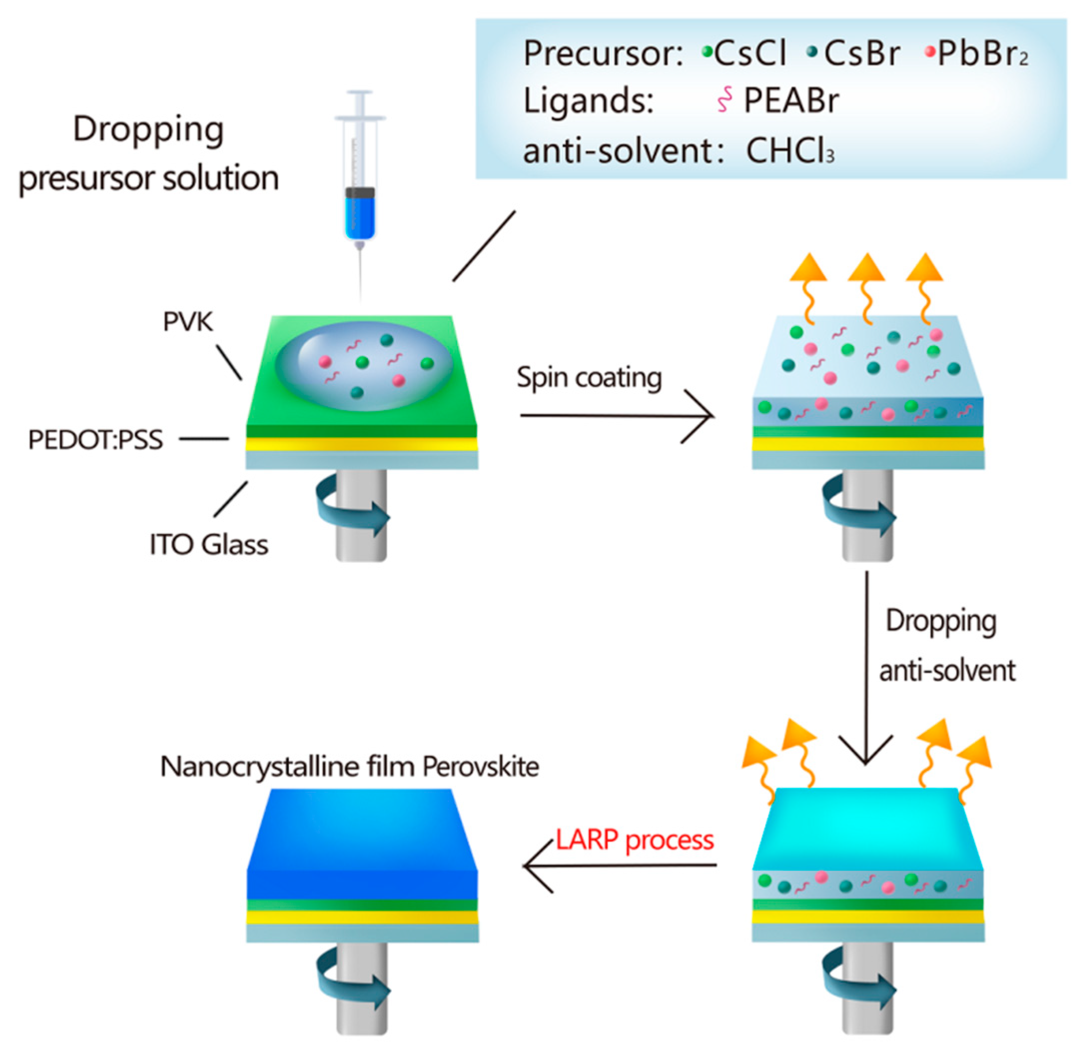
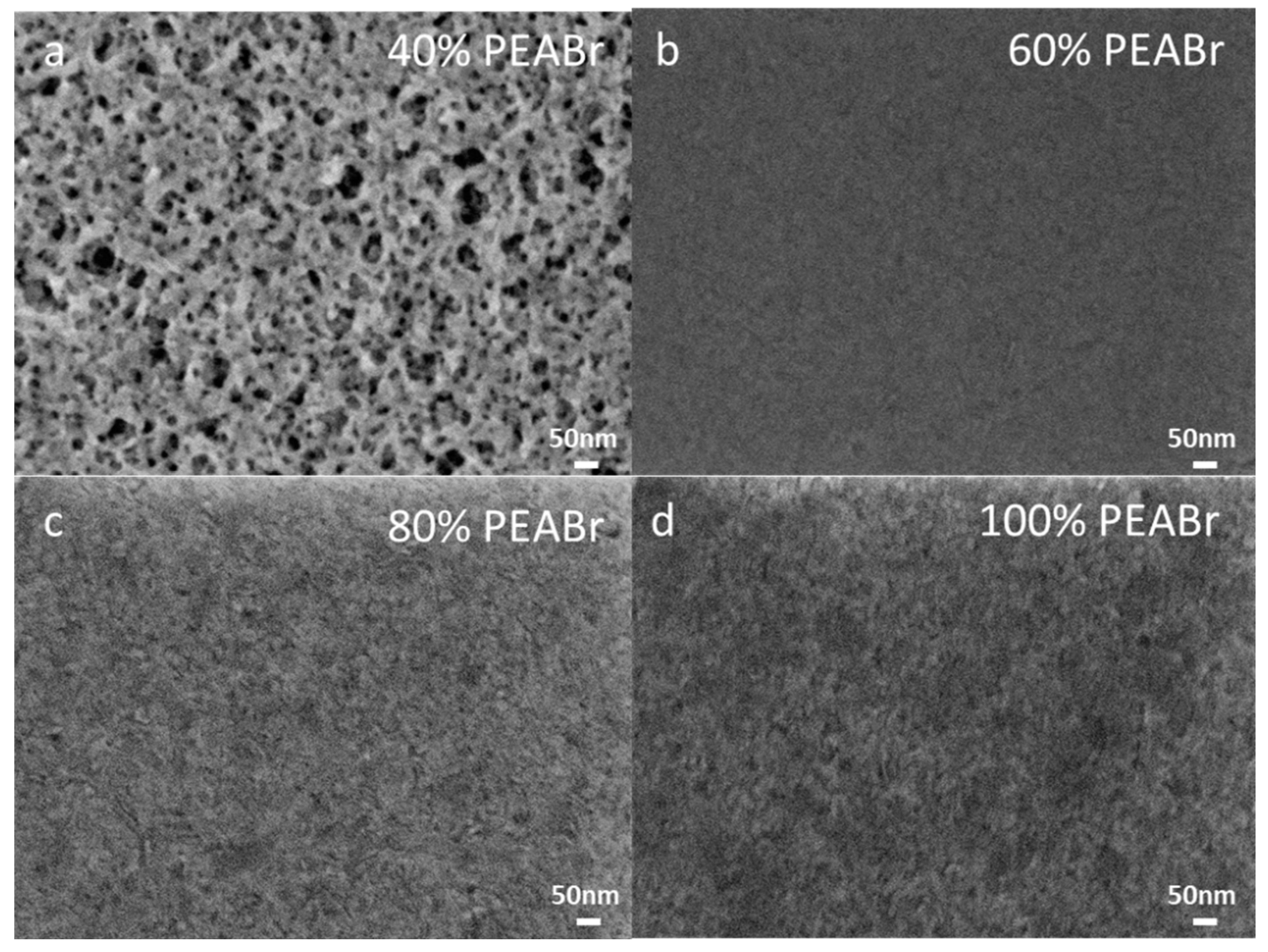
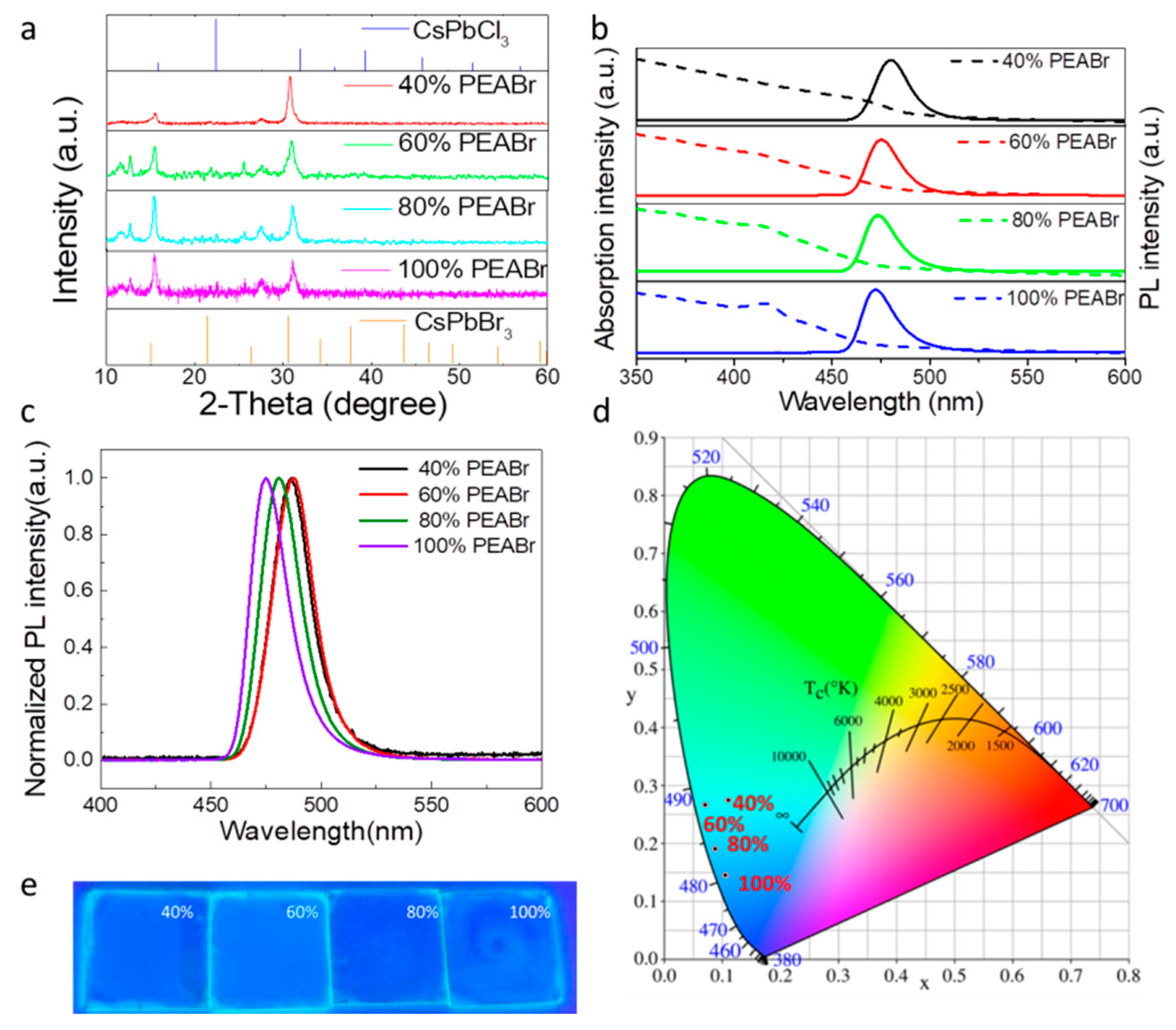
2.3. CsPbCl0.75Br2.25 Perovskite Nanocrystals (PNCs) Film Fabrication

All of the CsPbCl0.75Br2.25 PNCs films were fabricated on the PVK films. The different perovskite solution was spin-coated at 2500 rpm for 120 s and 200 uL trichloromethane was dropped on the spinning substrate after 30 s from the beginning of film rotation. In the process, the pipette head was completely perpendicular to the surface of the perovskite film. In order to prevent sputtering solution, the pipette head should be as close to the film as possible and should not touch the film surface. Then, it was dried at 80 °C for 5 min to remove residual solvent and ensure the complete reaction of the precursors. All of the above experiments were finished in a nitrogen filled glovebox.

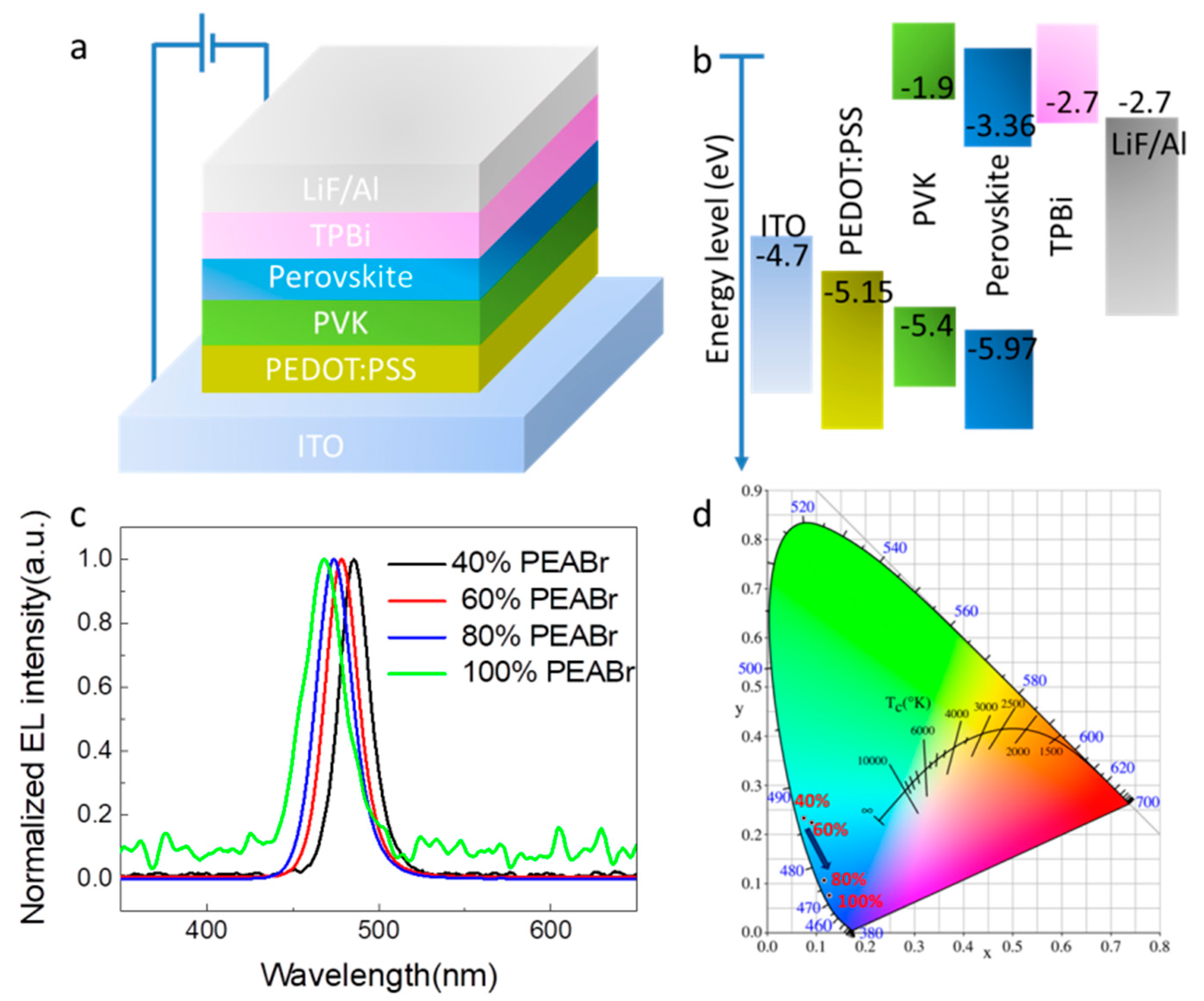
2.4. LED Device Fabrication

The patterned ITO-coated glass substrates cleaned with detergent were sequentially cleaned in deionized water, acetone, ethanol, and deionized water by sonication for 15 min. After a 9 min O2 plasma treatment for ITO, PEDOT: PSS was spin-coated on the substrate at 3500 rpm for 60 s, followed by annealing at 150 °C for 15 min in ambient air. Then, PVK (10 mg/mL in THF) was spin-coated on the PEDOT: PSS film at 4000 rpm for 40 s and baked at 120 °C for 30 min. PVK film was then treated with O2 plasma for 15 min. Then, the substrates were transferred to a nitrogen-filled glovebox. Different DMSO precursor solutions were spin-coated on top of the PVK film to fabricate the CsPbCl0.75Br2.25 PNC films, as carried out previously. Finally, TPBi (20 nm), LiF (1 nm), and the Al electrode (100 nm) were deposited using a thermal evaporation system.

2.5. Device Measurements and Film Characterization
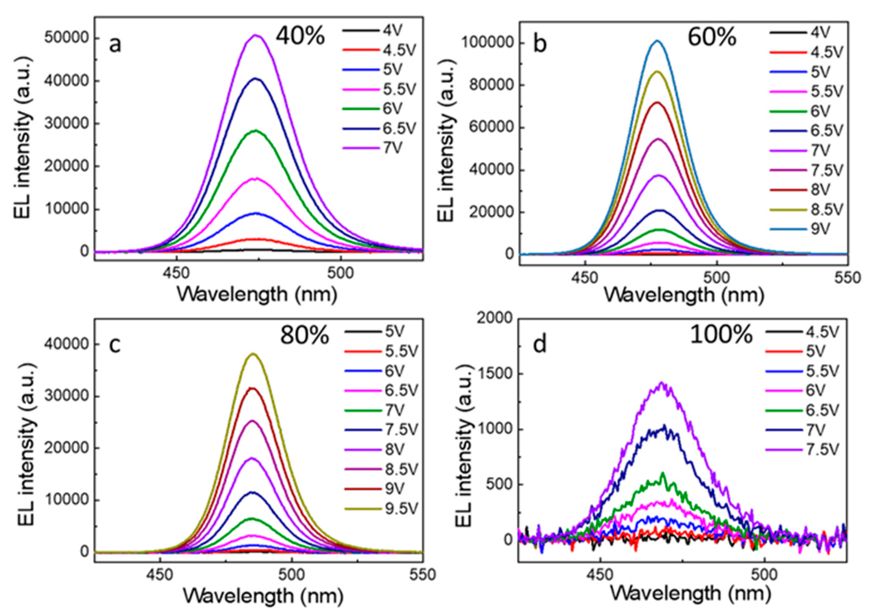
The morphology and energy-dispersive X-ray results of the perovskite films with different ratios of PEABr were obtained using field emission scanning electron microscopy (FE-SEM, Hitachi, Tokyo, Japan, SACS 4800). The voltage here is 5 KV, the working distance is 6900 um, and the emission current here is 1900 nA. A Nikon microscopy apparatus was applied to take the PL images of the perovskite films. Absorption and PL spectra at 360 nm excitation were evaluated at an indoor temperature under a xenon lamp at 150 W by a UV-3101 spectrophotometer and Hitachi F-7000 fluorescence spectrofluorometer, respectively. X-ray diffraction (XRD) patterns were characterized by the perovskite films by D8 Focus X-ray diffractometer purchased from Bruker Company. The 2θ Angle range of data acquisition during measurement was 10° to 80°, and 10° to 60° were captured for analysis. The Cu target was used as the radiation source. The radiation line Kα is λ = 1.54056 A. The operating voltage and current were 40 kV and 30 mA. The XRD step size was 0.02°, and the structure was confirmed to be a cubic crystal system by comparing with the standard card. Density—voltage characteristics, current efficiency—current density characteristics and power efficiency—voltage characteristics. The electroluminescence spectrum of the device was collected with Maya 2000 PRO spectrometer and the current-voltage-brightness and current-efficiency current-density characteristics of the device were tested by our self-built system. The test system includes: photometer, Geely voltage source and computer. A photometer (Konica Minolta LS-110, Tokyo, Japan) was used to record the brightness of the device. A Geely Time voltage source (Keithley 2400, Cleveland, OH, USA) acted as the voltage source of the device and tested the current flowing through the device. Finally, the software was used to read and record the brightness, voltage and current of the device, and calculate the current of the LED. The results of EQE were obtained from the system of the integrating sphere combined with the Ocean Optics spectrum-photometer.

3. Results

Herein, a blue-emission perovskite film with CsPbCl0.75Br2.25 perovskite nanocrystals (PNCs) were prepared based on in situ LARP technology. Figure 1 schematically illustrates the in situ fabrication process of CsPbCl0.75Br2.25 PNC films. LARP has been demonstrated to be a versatile method to fabricate PNCs toward a highly efficient cladding solution by mixing the precursors in polar solvents with non-polar solvents. During the precipitation process, the change in solubility caused the nucleation process. The nucleation process resulted in differences in crystal size and crystal homogeneity compared with ordinary preparation methods. The in situ LARP method can typically produce smaller and more uniform crystals. Typically, in situ fabrication on a substrate for PeLEDs involves two steps: spin-coating a precursor solution in polar solvents (usually dimethylformamide, DMF or DMSO) and then dropping the anti-solvent at an appropriate time [9].
In order to obtain high-performance blue PeLEDs, high-quality and uniform-thickness CsPbCl0.75Br2.25 PNC films are essential. In this work, we introduced PEABr as the ligand for the preparation of perovskite films, and DMSO was selected as the solvent to disperse the perovskite precursor, and chloroform was selected as the anti-solvent to induce the reaction processes. The scanning electron microscope (SEM) images of the perovskite films with different ratios of PEABr including 40%, 60%, 80% and 100% are shown in Figure 2. The SEM images of the perovskite films without PEABr are shown in Figure S1. With the increase in the amount of PEABr to 60%, a regular perovskite small crystal was obtained. Moreover, the perovskite film became more uniform and denser. This means that the introduction of PEABr can effectively regulate the formation of perovskite films. However, with the continuous increase in the amount of macromolecular ligand PEABr to 100%, the excessive addition of PEABr led to phase separation between PEABr and perovskite. The perovskite crystal returned to its irregular shape, resulting in a poorer crystal quality perovskite film [10,16]. The film quality can also be observed from the comment spectra. As shown in Table 1, the films with 60% PEABr had the strongest emission intensity and the smallest FWHM. This indicates that the nanocrystal size of the film was the most uniform, the film was well passivated and the occurrence of non-radiative recombination was weakened. As shown in Table S1 (Supplementary Material), the Photoluminescence quantum yield (PLQY) of the film was also enhanced with the increase in PEABr and then weakened due to the excess of PEABr.
The structure and properties of the perovskite films have been studied by X-ray diffraction (XRD), as shown in Figure 3a. In the original CsPbCl0.75Br2.25 film, a main peak appeared at 2θ angle of 15.4°, corresponding to the (100) plane of the 3D perovskite. A main peak appeared at 2θ angle of 30.8°, corresponding to the (200) plane of the 3D perovskite. With the increase in PEABr content, the crystal peak intensity of (200) decreased, while that of (100) increased. These results indicate that the PEABr can induce CsPbCl0.75Br2.25 perovskite crystal to grow oriented in (100) direction. The perovskite film was identified as CsPbBr3 and CsPbCl3 according to the standard card. As shown in Figure S4, we calculated and measured the lattice sizes of 0.290 nm and 0.283 nm in TEM images, corresponding to the (200) sides of the CsPbBr3 (0.2915 nm). Additionally, the lattice sizes of 0.231 nm corresponded to the (211) sides of the CsPbBr3 (0.238 nm) and CsPbCl3 (0.2288 nm). The absorption and PL spectra were measured and are shown in Figure 3b. It can be implied that with the increase in the amount of PEABr, the absorption and PL peaks gradually shifted to a short wavelength. The same trend based on the normalized PL measurements can be found in Figure 3c. With the increase in the proportion of perovskite generation, the wavelength of the PL peak blue shifted from 488 nm to 475 nm. It is worth noting that there should be several specific emission peaks if they were composed of different types of 2D perovskites, as reported in the previous work [31]. Here, the PL peaks present significant Gaussian distribution without the characteristic peaks of two-dimensional perovskites. From Figure 3d, the corresponding Commission Internationale de L’E chlaiage (CIE), Vienna, Austria coordinates agree well with the color change. The images of the blue perovskite films with the amount of PEABr ligand, increased from 40% to 60%, 80% and 100% under 365 nm light irradiation, are shown in Figure 3e. The colors of the perovskite films are obviously blue; moreover, the chemical composition of the synthesized CsPbCl0.75Br2.25 PNCs was analyzed via energy dispersive spectrometer (EDS) spectroscopy. As shown in Figure S2 (Supplementary Material) and Figure S3 (Supplementary Material), elements of Br, Pb, Cl and Cs are confirmed, indicating CsPbCl0.75Br2.25. As shown in Table S3 (Supplementary Material), the atom molar ratio of Cl to Br is about 1:3, which fits to the data of our pre-design CsPbCl0.75Br2.25 PNCs. These results demonstrated the successful synthesis of the CsPbCl0.75Br2.25 PNCs via our method.
Encouraged by the above results, we further fabricated the blue PeLEDs using perovskite films with different ratios of PEABr and a device structure of ITO/PEDOT: PSS/PVK/perovskite film/TPBi/LiF/Al, as indicated in Figure 4a. Their corresponding energy levels of the composed layers are shown in Figure 4b. The normalized EL spectrum of the blue PeLEDs by adding different ratios of PEABr were detected under 6 V, as shown in Figure 4c. The results showed that with the increase in PEABr content, the peak of the EL spectrum shifted from 485 nm to 468 nm, which was closely consistent with the results of the PL spectra. With the blue shift in EL spectra, the corresponding CIE value also changed from the sky-blue to pure-blue region, which meets the requirement of broad color gamut display. Figure 5 and Table 2 summarize the electrical properties of the devices prepared with different proportions of PEABr CsPbCl0.75Br2.25 thin films. It can be seen from Figure 5b that the working voltage of PeLED with different proportions of PEAB can be at least about 4 V, which conforms to the condition of the low working voltage of the device, indicating that the balance of PeLED carrier injection is excellent. We found that higher brightness (1069 cd/m2, Figure 5b, Table 2) was achieved through 60% PEABr addition. The best EQEs and current efficiency (CE) of 2.65% and 1.92 cd/A were found in device with 60% PEABr. The EL properties of the perovskite films are closely related to the trap density of the perovskite film. The higher the trap density is, the more severe traps, resulting in more severe non-radiation trap-assisted recombination. Due to the large number of pinholes in the pristine perovskite film, the introduction of ligand PEABr led to a better coverage and crystal quality. In other words, the introduction of 40% and 60% PEABr can effectively inhibit the current leakage. However, when the concentration of PEABr is further increased to 80% or 100%, the crystal quality of the thin films decreases compared with that of 60% PEABr. This is because excessive PEABr leads to phase separation with perovskite, so the PeLED performance also decreases.
When the content of PEABr is 60%, the perovskite film had the most excellent film morphology. The SEM and transmission electron microscope (TEM) of the superior morphological information is shown in Figure 2b and Figure S4 (Supplementary Material). We can see that the dimeter of the CsPbCl0.75Br2.25 PNCs is about 10 nm from Figure S4 (Supplementary Material). Figure S3c (Supplementary Material) and Figure S3d (Supplementary Material) show the spacings of the CsPbCl0.75Br2.25 PNCs, which is consistent with the previously measured XRD performance. Based on the high-quality film morphology, the prepared blue LED device has the superior electrical properties, which is shown in Figure 5. We measured the values of current density versus voltage in Figure 5a. As shown in Figure 6b, we observed 8.8 V, as shown in Figure 5c. From Figure 5d, we can calculate the EQE of the LED devices, in which the largest value is 2.65% on the voltage of 8.8 V. These results demonstrated the blue emitting PeLED has the predominant electrical properties. The blue emitting PeLED is shown in Figure S5 (Supplementary Material). Last but not least, the blue emitting PeLED still has a relatively high value of EQE on a comparatively high voltage.
Figure 6 shows the EL spectra of PeLEDs with different PEABr content under different operating voltages obtained recorded by a fiber optic spectrometer. It is notable that the position of the EL peak does not shift with the increase in voltage. Even at a driving voltage of 9 V, the device still shows good spectral stability. Figure S6 (Supplementary Material) shows that the EL spectra of ordinary devices without a PVK layer were significantly red shifted with increasing voltage, which is attributed to the perovskite phase with large n induced by PEDOT: PSS layer [31]. We also present the max EL intensity comparison of 60% PEABr at different voltages with or without the PVK layer in Table S3 (Supplementary Material). The electroluminescence performance of the PeLED with the PVK layer is much better than that without the PVK layer, especially at high pressure. The introduction of the PVK hole transport layer in the device can effectively isolate the PEDOT: PSS layer and luminescence layer, which can reduce or even eliminate the adverse induction of the PEDOT: PSS layer to the luminescence layer and successfully inhibit halide atom migration. In addition, the PVK layer with hydrophobic properties can provide environmental stability and effectively inhibit the non-radiative recombination of the metal halide luminescent layer. Combined with the high-quality thin film prepared by in situ LARP method such as luminescent layer, the PeLEDs finally shows excellent spectral stability.

4. Conclusions

In summary, we have realized stable and efficient blue PeLED emission at 478 nm using the ligand-assisted reprecipitation method. The maximum brightness is 1069 cd/m2 and the greatest EQE is 2.65%. The introduction of PEABr can effectively passivate the defect states on the surface of the perovskite film, making the perovskite film more compact. With the increase in PEABR, the PL peaks shift to a short wavelength. By introducing the PVK hole transport layer, the device can obtain efficient hole injection. The PVK layer with hydrophobic properties can provide environmental stability and can effectively isolate the PEDOT: PSS layer and luminescence layer and, thus, inhibit halide atom migration. Consequently, the EL peaks of the devices made by our method do not shift as the voltage increases. In other words, the devices have suitable spectral stability even at a high voltage, which is attributed to the combined effect of the PEABr and PVK layer. This overcomes the fatal shortcoming of voltage instability caused by an unstable power spectrum and greatly improves the application value and prospect of blue PeLEDs.

Supplementary Materials

The following are available online at https://www.mdpi.com/article/10.3390/nano12172906/s1, Figure S1: The SEM images of the perovskite films without PEABr; Figure S2: Energy dispersive spectrometer (EDS) spectrum of the CsPbCl0.75Br2.25 PNCs with different ratios of PEABr; Figure S3: Energy dispersive spectrometer mapping image of the CsPbCl0.75Br2.25 PNCs with 60% ratios of PEABr; Figure S4: top-view transmission electron microscope (TEM) images of perovskite thin films with 60% ratios of PEABr; Figure S5: CsPbCl0.75Br2.25 PeLEDs with 60% ratios of PEABr in in daylight and the darkness; Figure S6: The EL spectra of the PeLEDs without PVK layer and with 60% ratios of PEABr; Table S1: The optical properties of CsPbCl0.75Br2.25 films with different ratios of PEABr; Table S2: Element composition of Br, Pb, Cl and Cs atoms of the CsPbCl0.75Br2.25 PNCs samples calculated by the EDS results from Figure S1; Table S3: The max EL intensity comparison of 60% PEABr at different voltages with or without PVK layer.

Author Contributions

Methodology, Y.S. (Ying Su); software, H.Z., Y.S. (Ying Su) and X.X.; formal analysis, H.Z.; data curation, H.Z., W.Y. and Y.S. (Yifang Sun); writing—original draft preparation, H.Z.; writing—review and editing, H.Z., Q.Z. and Y.S. (Ying Su); supervision, Q.Z., W.J., K.Z. and X.L.; project administration, Q.Z. All authors have read and agreed to the published version of the manuscript.

Funding

This work was supported by the Science and Technology Development Project of Jilin Province under Grant No. 20180201057YY and No. 20160101231JC, and the program of the National Natural Science Foundation of China (No. 11974141, 1207414 and 62105054), and Student Innovation Training Program of CIOMP, and the Fundamental Research Funds for the Central Universities (DUT22YG117).

Data Availability Statement

Not applicable.

Conflicts of Interest

The authors declare no conflict of interest.

References

  1. Protesescu, L.; Yakunin, S.; Bodnarchuk, M.I.; Krieg, F.; Caputo, R.; Hendon, C.H.; Yang, R.X.; Walsh, A.; Kovalenko, M.V. Nanocrystals of Cesium Lead Halide Perovskites (CsPbX(3), X = Cl, Br, and I): Novel Optoelectronic Materials Showing Bright Emission with Wide Color Gamut. Nano Lett. 2015, 15, 3692–3696. [Google Scholar] [CrossRef] [Green Version]
  2. Su, Y.; Chen, X.; Ji, W.; Zeng, Q.; Ren, Z.; Su, Z.; Liu, L. Highly Controllable and Efficient Synthesis of Mixed-Halide CsPbX3 (X = Cl, Br, I) Perovskite QDs toward the Tunability of Entire Visible Light. ACS Appl. Mater. Interfaces 2017, 9, 33020–33028. [Google Scholar] [CrossRef] [PubMed]
  3. Li, X.; Wu, Y.; Zhang, S.; Cai, B.; Gu, Y.; Song, J.; Zeng, H. CsPbX3Quantum Dots for Lighting and Displays: Room-Temperature Synthesis, Photoluminescence Superiorities, Underlying Origins and White Light-Emitting Diodes. Adv. Funct. Mater. 2016, 26, 2435–2445. [Google Scholar] [CrossRef]
  4. Yang, X.; Zhang, X.; Deng, J.; Chu, Z.; Jiang, Q.; Meng, J.; Wang, P.; Zhang, L.; Yin, Z.; You, J. Efficient green light-emitting diodes based on quasi-two-dimensional composition and phase engineered perovskite with surface passivation. Nat. Commun. 2018, 9, 570. [Google Scholar] [CrossRef] [PubMed]
  5. Wang, H.; Zhang, X.; Wu, Q.; Cao, F.; Yang, D.; Shang, Y.; Ning, Z.; Zhang, W.; Zheng, W.; Yan, Y.; et al. Trifluoroacetate induced small-grained CsPbBr3 perovskite films result in efficient and stable light-emitting devices. Nat. Commun. 2019, 10, 665. [Google Scholar] [CrossRef] [PubMed] [Green Version]
  6. Song, J.; Li, J.; Li, X.; Xu, L.; Dong, Y.; Zeng, H. Quantum Dot Light-Emitting Diodes Based on Inorganic Perovskite Cesium Lead Halides (CsPbX3). Adv. Mater. 2015, 27, 7162–7167. [Google Scholar] [CrossRef]
  7. Jeong, C.H.; Kim, P.S.H.; Wolf, M.H.; Lee, Y.H.; Heo, C.; Sadhanala, C.L.; Myoung, J.H.; Yoo, A.; SeunghyupIm, N.S.; Friend, S.H.; et al. Overcoming the electroluminescence efficiency limitations of perovskite lightemitting diodes. Science 2015, 350, 1222–1225. [Google Scholar]
  8. Chiba, T.; Hayashi, Y.; Ebe, H.; Hoshi, K.; Sato, J.; Sato, S.; Pu, Y.-J.; Ohisa, S.; Kido, J. Anion-exchange red perovskite quantum dots with ammonium iodine salts for highly efficient light-emitting devices. Nat. Photonics 2018, 12, 681–687. [Google Scholar] [CrossRef]
  9. Han, D.; Imran, M.; Zhang, M.; Chang, S.; Wu, X.G.; Zhang, X.; Tang, J.; Wang, M.; Ali, S.; Li, X.; et al. Efficient Light-Emitting Diodes Based on in Situ Fabricated FAPbBr3 Nanocrystals: The Enhancing Role of the Ligand-Assisted Reprecipitation Process. ACS Nano 2018, 12, 8808–8816. [Google Scholar] [CrossRef]
  10. Cao, Y.; Wang, N.; Tian, H.; Guo, J.; Wei, Y.; Chen, H.; Miao, Y.; Zou, W.; Pan, K.; He, Y.; et al. Perovskite light-emitting diodes based on spontaneously formed submicrometre-scale structures. Nature 2018, 562, 249–253. [Google Scholar] [CrossRef]
  11. Lin, K.; Xing, J.; Quan, L.N.; de Arquer, F.P.G.; Gong, X.; Lu, J.; Xie, L.; Zhao, W.; Zhang, D.; Yan, C.; et al. Perovskite light-emitting diodes with external quantum efficiency exceeding 20 per cent. Nature 2018, 562, 245–248. [Google Scholar] [CrossRef] [PubMed]
  12. Zhao, B.; Bai, S.; Kim, V.; Lamboll, R.; Shivanna, R.; Auras, F.; Richter, J.M.; Yang, L.; Dai, L.; Alsari, M.; et al. High-efficiency perovskite–polymer bulk heterostructure light-emitting diodes. Nat. Photonics 2018, 12, 783–789. [Google Scholar] [CrossRef]
  13. Xu, W.; Hu, Q.; Bai, S.; Bao, C.; Miao, Y.; Yuan, Z.; Borzda, T.; Barker, A.J.; Tyukalova, E.; Hu, Z.; et al. Rational molecular passivation for high-performance perovskite light-emitting diodes. Nat. Photonics 2019, 13, 418–424. [Google Scholar] [CrossRef]
  14. Shen, Y.; Cheng, L.P.; Li, Y.Q.; Li, W.; Chen, J.D.; Lee, S.T.; Tang, J.X. High-Efficiency Perovskite Light-Emitting Diodes with Synergetic Outcoupling Enhancement. Adv. Mater. 2019, 31, e1901517. [Google Scholar] [CrossRef] [PubMed]
  15. Li, G.; Rivarola, F.W.; Davis, N.J.; Bai, S.; Jellicoe, T.C.; de la Pena, F.; Hou, S.; Ducati, C.; Gao, F.; Friend, R.H.; et al. Highly Efficient Perovskite Nanocrystal Light-Emitting Diodes Enabled by a Universal Crosslinking Method. Adv. Mater. 2016, 28, 3528–3534. [Google Scholar] [CrossRef]
  16. Li, Z.; Chen, Z.; Yang, Y.; Xue, Q.; Yip, H.L.; Cao, Y. Modulation of recombination zone position for quasi-two-dimensional blue perovskite light-emitting diodes with efficiency exceeding 5. Nat. Commun. 2019, 10, 1027. [Google Scholar] [CrossRef]
  17. Hoye, R.L.Z.; Lai, M.L.; Anaya, M.; Tong, Y.; Galkowski, K.; Doherty, T.; Li, W.; Huq, T.N.; Mackowski, S.; Polavarapu, L.; et al. Identifying and Reducing Interfacial Losses to Enhance Color-Pure Electroluminescence in Blue-Emitting Perovskite Nanoplatelet Light-Emitting Diodes. ACS Energy Lett. 2019, 4, 1181–1188. [Google Scholar] [CrossRef]
  18. Fang, T.; Zhang, F.; Yuan, S.; Zeng, H.; Song, J. Recent advances and prospects toward blue perovskite materials and light-emitting diodes. InfoMat 2019, 1, 211–233. [Google Scholar] [CrossRef] [Green Version]
  19. Cheng, L.; Cao, Y.; Ge, R.; Wei, Y.-Q.; Wang, N.-N.; Wang, J.-P.; Huang, W. Sky-blue perovskite light-emitting diodes based on quasi-two-dimensional layered perovskites. Chin. Chem. Lett. 2017, 28, 29–31. [Google Scholar] [CrossRef]
  20. Kumawat, N.K.; Dey, A.; Kumar, A.; Gopinathan, S.P.; Narasimhan, K.L.; Kabra, D. Band Gap Tuning of CH(3)NH(3)Pb(Br(1-x)Clx)(3) Hybrid Perovskite for Blue Electroluminescence. ACS Appl. Mater. Interfaces 2015, 7, 13119–13124. [Google Scholar] [CrossRef]
  21. Gangishetty, M.K.; Hou, S.; Quan, Q.; Congreve, D.N. Reducing Architecture Limitations for Efficient Blue Perovskite Light-Emitting Diodes. Adv. Mater. 2018, 30, e1706226. [Google Scholar] [CrossRef] [PubMed]
  22. Pan, J.; Quan, L.N.; Zhao, Y.; Peng, W.; Murali, B.; Sarmah, S.P.; Yuan, M.; Sinatra, L.; Alyami, N.M.; Liu, J.; et al. Highly Efficient Perovskite-Quantum-Dot Light-Emitting Diodes by Surface Engineering. Adv. Mater. 2016, 28, 8718–8725. [Google Scholar] [CrossRef] [PubMed]
  23. Hou, S.; Gangishetty, M.K.; Quan, Q.; Congreve, D.N. Efficient Blue and White Perovskite Light-Emitting Diodes via Manganese Doping. Joule 2018, 2, 2421–2433. [Google Scholar] [CrossRef] [Green Version]
  24. Yuan, M.; Quan, L.N.; Comin, R.; Walters, G.; Sabatini, R.; Voznyy, O.; Hoogland, S.; Zhao, Y.; Beauregard, E.M.; Kanjanaboos, P.; et al. Perovskite energy funnels for efficient light-emitting diodes. Nat. Nanotechnol. 2016, 11, 872–877. [Google Scholar] [CrossRef]
  25. Wang, N.; Cheng, L.; Ge, R.; Zhang, S.; Miao, Y.; Zou, W.; Yi, C.; Sun, Y.; Cao, Y.; Yang, R.; et al. Perovskite light-emitting diodes based on solution-processed self-organized multiple quantum wells. Nat. Photonics 2016, 10, 699–704. [Google Scholar] [CrossRef]
  26. Jiang, Y.; Qin, C.; Cui, M.; He, T.; Liu, K.; Huang, Y.; Luo, M.; Zhang, L.; Xu, H.; Li, S.; et al. Spectra stable blue perovskite light-emitting diodes. Nat. Commun. 2019, 10, 1868. [Google Scholar] [CrossRef] [Green Version]
  27. Yao, E.P.; Yang, Z.; Meng, L.; Sun, P.; Dong, S.; Yang, Y.; Yang, Y. High-Brightness Blue and White LEDs based on Inorganic Perovskite Nanocrystals and their Composites. Adv. Mater. 2017, 29, 1606859. [Google Scholar] [CrossRef] [PubMed]
  28. Ahmed, G.H.; El-Demellawi, J.K.; Yin, J.; Pan, J.; Velusamy, D.B.; Hedhili, M.N.; Alarousu, E.; Bakr, O.M.; Alshareef, H.N.; Mohammed, O.F. Giant Photoluminescence Enhancement in CsPbCl3 Perovskite Nanocrystals by Simultaneous Dual-Surface Passivation. ACS Energy Lett. 2018, 3, 2301–2307. [Google Scholar] [CrossRef] [Green Version]
  29. Yong, Z.J.; Guo, S.Q.; Ma, J.P.; Zhang, J.Y.; Li, Z.Y.; Chen, Y.M.; Zhang, B.B.; Zhou, Y.; Shu, J.; Gu, J.L.; et al. Doping-Enhanced Short-Range Order of Perovskite Nanocrystals for Near-Unity Violet Luminescence Quantum Yield. J. Am. Chem. Soc. 2018, 140, 9942–9951. [Google Scholar] [CrossRef] [Green Version]
  30. Chen, Z.; Zhang, C.; Jiang, X.F.; Liu, M.; Xia, R.; Shi, T.; Chen, D.; Xue, Q.; Zhao, Y.J.; Su, S.; et al. High-Performance Color-Tunable Perovskite Light Emitting Devices through Structural Modulation from Bulk to Layered Film. Adv. Mater. 2017, 29, 1603157. [Google Scholar] [CrossRef]
  31. Xing, J.; Zhao, Y.; Askerka, M.; Quan, L.N.; Gong, X.; Zhao, W.; Zhao, J.; Tan, H.; Long, G.; Gao, L.; et al. Color-stable highly luminescent sky-blue perovskite light-emitting diodes. Nat. Commun. 2018, 9, 3541. [Google Scholar] [CrossRef] [PubMed] [Green Version]
  32. Ren, Z.; Wang, K.; Sun, X.W.; Choy, W.C.H. Strategies Toward Efficient Blue Perovskite Light-Emitting Diodes. Adv. Funct. Mater. 2021, 31, 2100516. [Google Scholar] [CrossRef]
  33. Zhang, L.; Long, R. Developments and challenges ahead in blue perovskite light-emitting devices. J. Energy Chem. 2022, 71, 2095–4956. [Google Scholar] [CrossRef]
Figure 1. Schematic illustration of the in situ LARP to fabricateCsPbCl0.75Br2.25 PNC films.
Nanomaterials 12 02906 g001
Figure 2. Top-view SEM images of perovskite thin films with (a) 40%, (b) 60%, (c) 80% and (d) 100% ratios of PEABr.
Nanomaterials 12 02906 g002
Figure 3. (a) XRD patterns, (b) absorption and PL spectra, (c) normalized PL spectra, and (d) corresponding CIE of CsPbCl0.75Br2.25 thin films with different ratios of PEABr. (e) Images of the blue perovskite films with different ratios of PEABr under 365 nm light irradiation.
Nanomaterials 12 02906 g003
Figure 4. (a) PeLED architecture. (b) Energy levels for different layers of the device. (c) EL spectra of PeLEDs with different ratios of PEABr. (d) CIE values of the EL spectra of PeLEDs.
Nanomaterials 12 02906 g004
Figure 5. Performance of CsPbCl0.75Br2.25 PeLEDs with different ratios of PEABr. (a) current density versus voltage, (b) luminance versus voltage, (c) current efficiency versus voltage, and (d) EQE versus voltage curves.
Nanomaterials 12 02906 g005
Figure 6. EL spectra of PeLEDs with (a) 40%, (b) 60%, (c) 80% and (d) 100% ratios of PEABr.
Nanomaterials 12 02906 g006
Table 1. Summary of CsPbCl0.75Br2.25 perovskite films with different ratios of PEABr.
PL (nm)The Max PL IntensityFWHM (nm)
40% PEABr48033,88621.8
60% PEABr47556,53720.4
80% PEABr47349,98420.7
100% PEABr47222,31622.6
Table 2. Summary of CsPbCl0.75Br2.25 PeLEDs with different ratios of PEABr.
CE (cd/A)Luminance (cd/m2)EQEEL (nm)FWHM (nm)
40% PEABr0.95846.9@10 V1.01@7 V48522
60% PEABr1.921069@9 V[email protected] V47823
80% PEABr1.06[email protected] V[email protected] V47424
100% PEABr0.23[email protected] V0.47@7 V46826
Publisher’s Note: MDPI stays neutral with regard to jurisdictional claims in published maps and institutional affiliations.

