Article

Tuning Schottky Barrier of Single-Layer MoS2 Field-Effect Transistors with Graphene Electrodes

Division of Electrical, Electronic and Control Engineering, Kongju National University, Cheonan 31080, Korea
Nanomaterials 2022, 12(17), 3038; https://doi.org/10.3390/nano12173038
Submission received: 4 August 2022 / Revised: 22 August 2022 / Accepted: 30 August 2022 / Published: 1 September 2022
(This article belongs to the Special Issue 2D Nanostructures for Optoelectronic and Green Energy Devices)

Abstract

:
Two–dimensional materials have the potential to be applied in flexible and transparent electronics. In this study, single-layer MoS2 field-effect transistors (FETs) with Au/Ti–graphene heteroelectrodes were fabricated to examine the effect of the electrodes on the electrical properties of the MoS2 FETs. The contact barrier potential was tuned using an electric field. Asymmetrical gate behavior was observed owing to the difference between the MoS2 FETs, specifically between the MoS2 FETs with Au/Ti electrodes and those with graphene electrodes. The contact barrier of the MoS2 FETs with Au/Ti electrodes did not change with the electric field. However, the contact barrier at the MoS2–graphene interface could be modulated. The MoS2 FETs with Au/Ti–graphene electrodes exhibited enhanced on/off ratios (~102 times) and electron mobility (~2.5 times) compared to the MoS2 FETs with Au/Ti electrodes. These results could improve the understanding of desirable contact formation for high-performance MoS2 FETs and provide a facile route for viable electronic applications.

1. Introduction

Two–dimensional (2D) materials have attracted significant attention as potential candidates for next-generation electronics [1,2]. Graphene is considered to be one of the most promising 2D materials because of its unique electrical, mechanical, and optical properties. However, the widespread use of graphene in viable electronic device applications is limited by its zero-bandgap property, which considerably decreases the on/off ratio [3,4,5,6]. To overcome this limitation, graphene nanoribbons [7,8], bilayer graphene [9,10,11,12], and modified device architectures, such as vertical tunneling transistors, have been developed [13,14]. Although these devices have improved the on/off ratio, other desirable properties, such as mobility and current density, have deteriorated. Thus, there is an urgent requirement for 2D materials, including transition metal dichalcogenides (TMDs), with an appropriate bandgap and reasonable mobility to replace graphene. MoS2 is one of the most promising TMDs because its bandgap is 1.3–1.8 eV depending on the number of layers. Single-layer MoS2 films have a direct bandgap of 1.8 eV, whereas multilayer MoS2 films have an indirect bandgap of 1.2 eV [15,16,17]. Owing to these unique properties, MoS2 has been intensively studied for electronic and optoelectronic applications. In recent years, it has become possible to synthesize large-area single-layer MoS2 via chemical vapor deposition (CVD) [18,19,20,21,22]. This has provided a major opportunity for next-generation electronic device applications. However, the contact barrier issue must be studied for electronic device applications of 2D materials [23,24]. Moreover, the performance of MoS2 field-effect transistors (FETs) is lower than the theoretically predicted performance [25]. This discrepancy has been explained on the basis of charged impurities and localized states in MoS2 [26,27,28]. Dominant scattering processes decrease carrier mobility. In addition, the contact at MoS2–metal electrode interfaces is a critical issue. A tunneling barrier that is formed at the interface of a metal contact in an MoS2 device [29] significantly reduces carrier mobility in single–layer MoS2. This is one of the main reasons for the poor performance of single-layer MoS2 FETs. Sulfur atoms mediate the hybridization between a contact metal and Mo atoms, resulting in the tuning of the bandgap [30]. Furthermore, the bandgap of single-layer MoS2 can be determined by the strength of the Mo–S covalent bonding [31]. Therefore, a systematic study of the effects of electrode materials on the performance of MoS2 FETs can help resolve this critical issue and find a reliable method of improving the electrical properties of MoS2 FETs. A charge accumulation region forms at metal–MoS2 interfaces when a metal contact is used. This generally leads to the formation of an interface electric dipole, which modifies the interface band alignment [30]. This results in poor contact and an unexpected contact barrier between the metal and MoS2. Owing to the challenges associated with metal electrodes, graphene has been considered as a suitable electrode material for MoS2 FETs. Graphene and single-layer MoS2 bond via van der Waals (vdW) forces, thereby creating a pristine interface. Furthermore, the contact barrier between graphene and MoS2 can be controlled by tuning the work function of graphene (4.5 eV), which is quite similar to that of MoS2 [32]. As the work function of graphene can be readily tuned by applying an electric field, graphene-based heterostructures have recently been studied in electronic devices [33,34,35,36]. For instance, the Schottky barrier formed between graphene and silicon can be tuned by approximately 200 meV as a function of the gate voltage [13]. Therefore, the contact barrier between graphene and MoS2 can be tuned by applying an electric field.
Herein, we report high-performance single–layer MoS2 FETs with graphene electrodes that exhibit a considerable enhancement in the on/off ratio (~102 times) and electron mobility (~2.5 times) compared to the MoS2 FETs with Au/Ti electrodes. We show that the contact barrier potential of the MoS2 FETs with graphene electrodes can be effectively tuned by applying an electric field. The work function of graphene becomes higher than that of MoS2 at a negative bias voltage, resulting in the formation of a Schottky barrier. Similarly, the work function of graphene becomes lower than that of MoS2 at a positive bias voltage, resulting in the formation of an ohmic barrier. The contact barrier between MoS2 and graphene can be easily tuned using graphene electrodes. Thus, the on/off ratio and electron mobility of the MoS2 FET can be improved by tuning the contact barrier.

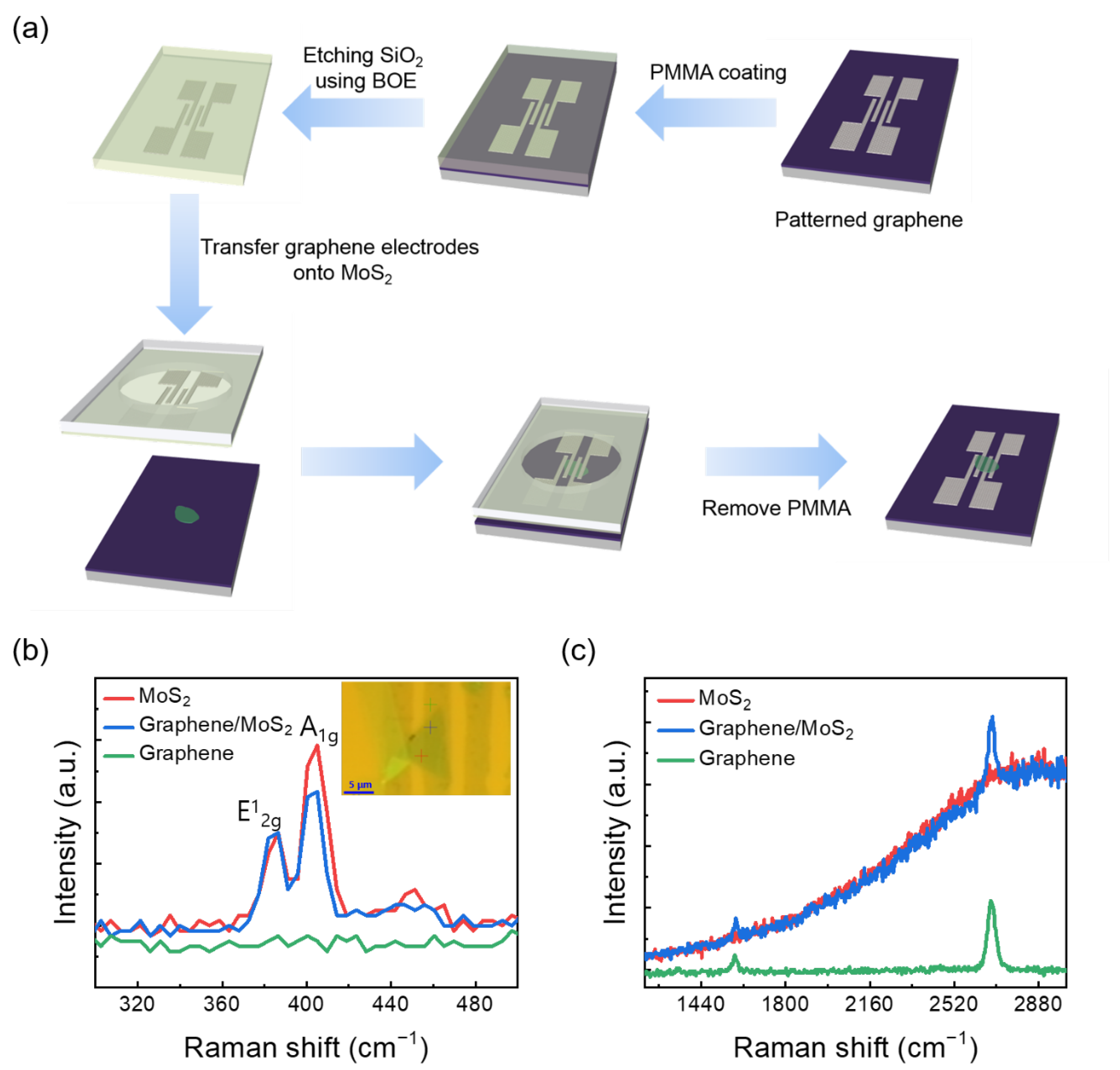
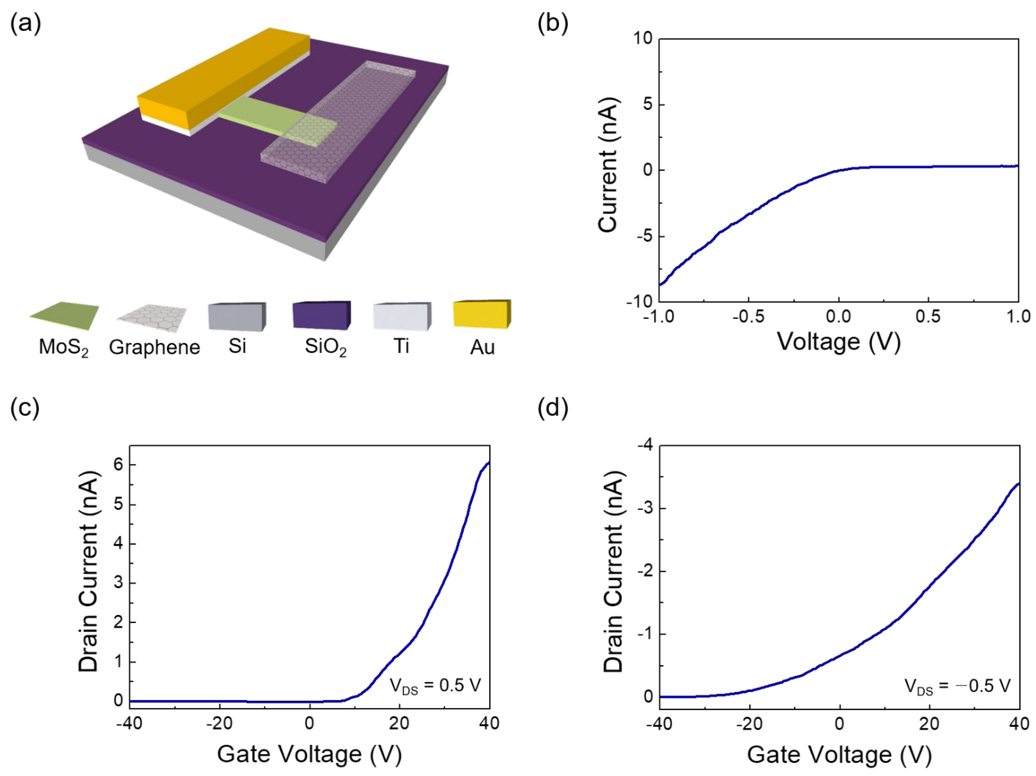
2. Materials and Methods

2.1. Graphene Growth and Transfer

Graphene was synthesized on a copper foil (99.8% purity, 0.025 mm thick, Alfa Aesar, Haverhill, MA, USA) using CVD at a growth temperature of 1050 °C with 10 sccm of H2 and 15 sccm of CH4 [37]. Then, the full side of the foil that faced upwards during synthesis was covered with poly(methyl methacrylate) (PMMA) (AR–N 7500.18, Allresist, Strausberg, Germany) via spin coating (4000 rpm for 60 s). The remaining graphene on the Cu foil that faced downwards during the synthesis was removed using O2 plasma (Femto, Diener, Ebhausen, Germany). The Cu foil was completely etched using 0.1 M ammonia persulfate (Sigma Aldrich, St. Louis, MO, USA). The PMMA/graphene layer was washed several times with fresh deionized water. Finally, the PMMA/graphene layer floated on the surface of the water, and it was transferred to a SiO2 substrate. The transferred PMMA/graphene layer was patterned using electron beam lithography (Nanobeam nB4, NBL, Cambridge, UK) as shown in Figure S1a.

2.2. Fabrication of the MoS2 Field-Effect Transistor

As shown in Figure S1b, single-layer MoS2 was prepared via mechanical exfoliation from a bulk MoS2 flake (429ML–AB, SPI Supplies, West Chester, PA, USA). To fabricate MoS2 FET with graphene electrode, a dry transfer process was employed [38]. Patterned graphene was transferred onto single–layer MoS2 flake after the alignment position using a micromanipulator (NMO–203, Narishige, Tokyo, Japan) (Figure 1a). Au/Ti electrodes were patterned using electron beam lithography with a positive electron beam resist (AR–P 671.04, Allresist, Strausberg, Germany). This was followed by metal deposition (Ti (5 nm)/Au (45 nm)) and a lift-off process.

2.3. Characterization of the MoS2 Thin Film and Field–Effect Transistor

Mechanical exfoliation was employed to extract high-quality single-layer MoS2 from bulk MoS2 [3]. Then, single–layer MoS2 was transferred onto a silicon wafer with a 300 nm thick SiO2 layer. Raman spectroscopy (Alpha 300R, WiTec, Ulm, Germany) was used to determine the number of layers of MoS2 [39]. The Raman spectrum of MoS2 revealed a peak spacing of less than 20 cm−1 between the E2g and A1g modes, indicating that single-layer MoS2 was formed. A 532 nm laser with a power of 1 mW was used as an excitation source. The exposure time was 1 s, and calibration was performed using a reference Si peak position of 520 cm−1. The fabricated MoS2 FETs were loaded into a vacuum chamber (Lake Shore) for electrical measurements. The electrical properties of the MoS2 FETs with graphene–graphene electrodes, Au/Ti–Au/Ti electrodes, and graphene–Au/Ti electrodes were characterized in vacuum (under 10−4 Torr) using a semiconductor parameter analyzer (4200-SCS with a preamplifier unit, Keithley, Cleveland, OH, USA) for comparison.

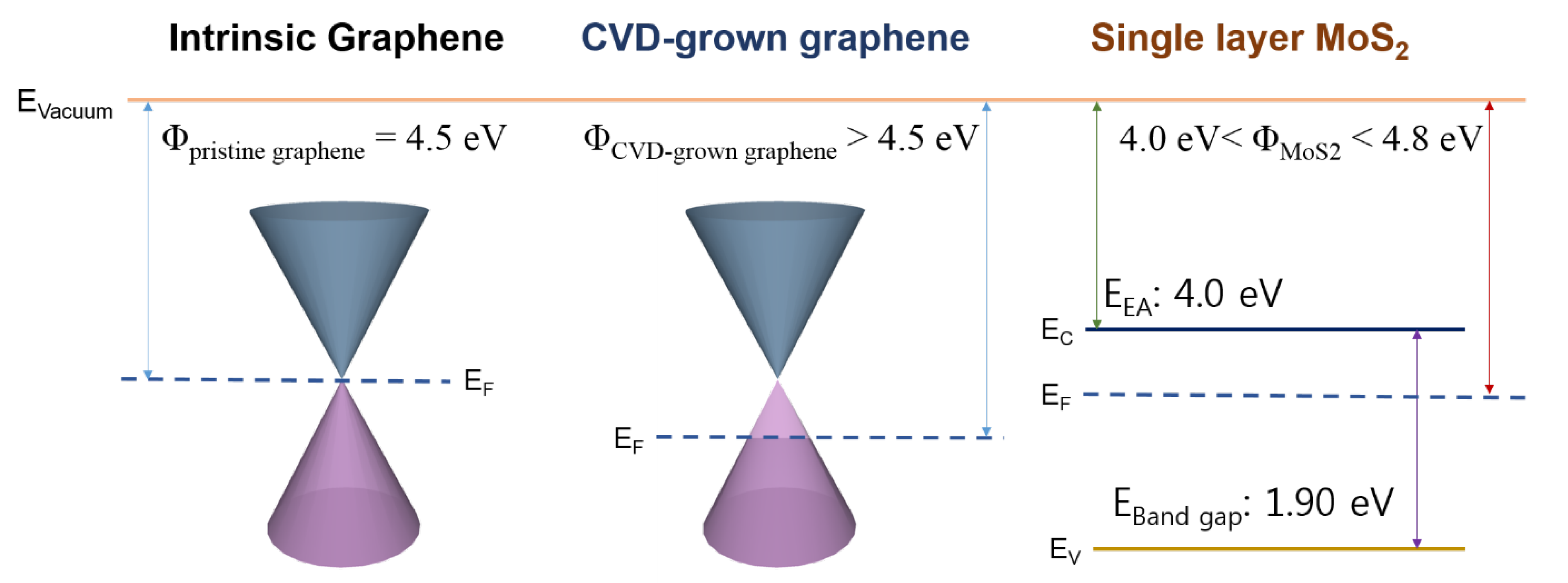
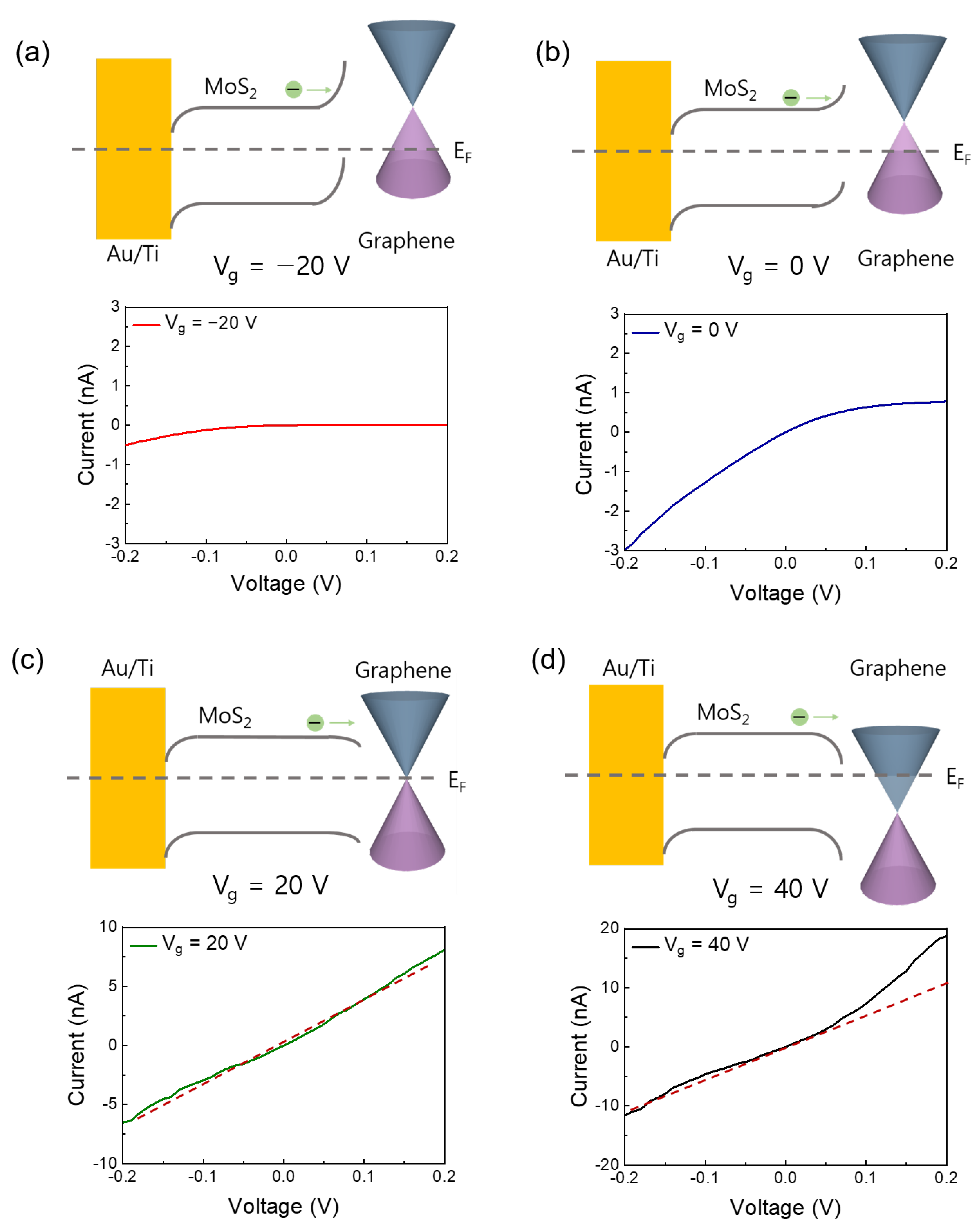
3. Results and Discussion

Figure 1b,c show the Raman spectra of single-layer MoS2, graphene on single-layer MoS2, and graphene, respectively. The MoS2 and graphene/MoS2 layers exhibit typical single-layer Raman active modes (~18.27 cm−1 of frequency difference between E2g and A1g), and the 2D/G ratio of graphene is about 4.06. Therefore, it can be noted that exfoliated MoS2 flake has a formation of single layer. The Dirac point of intrinsic graphene is at zero gate voltage, the work function of which is approximately 4.5 eV [32]. As shown in Figure S2, the Dirac point of the CVD-grown graphene electrode was measured at 22.5 V, owing to the hole doping originated from both coupling with dielectric layer of SiO2 and exposure to oxygen and moisture [40]. The schematic of the band structure of graphene and MoS2 is shown in Figure 2. Graphene and single-layer MoS2 were bonded via weak vdW forces. However, MoS2 and the metal interfaces formed covalent interactions, causing a change in the electronic structure [30]. This led to unexpected contact resistance. Three different types of single-layer MoS2 FETs were fabricated to investigate the effects of the graphene electrode. The first was a single-layer MoS2 FET with a Au/Ti–graphene heteroelectrode, as shown in Figure 3a. Highly boron-doped Si (resistance of 0.001 Ω) with a 300 nm thick SiO2 layer was used as the substrate. The channel length and width of the mechanically exfoliated MoS2 used in the single-layer MoS2 FET were ~2 μm and ~4 μm, respectively. Figure 3b shows the asymmetric IDS–VDS output characteristics of the single-layer MoS2 FET with the Au/Ti–graphene heteroelectrode without the gate voltage. Different contact barriers were generated according to the contact material. An ohmic contact was formed between single-layer MoS2 and Au/Ti. A Schottky contact was formed between single-layer MoS2 and graphene. Figure 3c shows the IDS–Vg transfer characteristics for a positive source–drain voltage (VDS). The on/off ratio and electron mobility (graphene in the heteroelectrode) were >105 and ~3.2 cm2/V∙s, respectively. Figure 3d shows the IDS–Vg transfer characteristics for a negative drain voltage. The on/off ratio and electron mobility (Au/Ti in the heteroelectrode) were >102 and ~1.2 cm2/V∙s, respectively. These results indicated that graphene could be used as an ideal electrode in a single-layer MoS2 FET. Mobility was calculated using the following equation: μ e = g m × L /   C g × V D × W ; where g m is the transconductance, V D is the source–drain voltage, L is the channel length, W is the channel width, and   C g is the capacitance of 300 nm thick SiO2. The MoS2 FET with the Au/Ti electrodes exhibited ohmic contact behavior, whereas the MoS2 FET with the graphene electrodes exhibited Schottky contact behavior. Multilayer MoS2 FETs with exfoliated graphene electrodes also showed ohmic contact behavior [41]. The work function of graphene was approximately 4.5 eV because mechanically exfoliated graphene was almost pure with no doping. Therefore, the single-layer MoS2 FET with the graphene electrodes exhibited a Schottky barrier without a gate bias voltage. However, the work function of graphene was electrostatically adjusted to approximately 300 meV for single-layer graphene by tuning the Fermi level (EF) by changing the gate voltage by 50 V [32]. The work function of graphene decreased at a positive gate bias voltage. Figure 4 shows the IDS–VDS characteristics of the single-layer MoS2 FET as a function of the back-gate voltage. The Schottky barrier between graphene and single-layer MoS2 was enhanced at a negative gate voltage; thus, current could not flow in the negative gate voltage direction (Figure 4a). As the gate was positively biased, the Schottky barrier between graphene and single-layer MoS2 decreased, and the contact barrier between single-layer MoS2 and Au/Ti did not change. The IDS–VDS output characteristics of the single-layer MoS2 FET with the Au/Ti–graphene heteroelectrode (green solid line) showed almost similar with linear (red dashed line) at a gate voltage of 20 V because the work function of graphene became similar to that of single-layer MoS2 (Figure 4c). As the gate voltage exceeded 20 V, the current level (black solid line) of the graphene electrode became higher than that of the Au/Ti electrode (Figure 4d). These results showed that the electrical properties of the single-layer MoS2 FET were enhanced using the graphene electrodes. A Schottky barrier was formed at the interface of graphene and MoS2 in the current-off region; thus, there was no leakage current. However, an ohmic barrier was formed at the interface between graphene and MoS2 in the current-on region. Therefore, the on/off ratio and electron mobility of single-layer MoS2 were high. The on/off ratio and electron mobility of single–layer MoS2 were compared with those of homogeneous electrodes. A single-layer MoS2 FET with the graphene electrodes was fabricated, and its electrical properties were measured. Figure 5a shows the schematic of the single-layer MoS2 FET with the graphene electrodes, and Figure 5b shows its IDS–Vg transfer characteristics. The IDS–VDS output characteristics shown in Figure 5c confirmed that a Schottky barrier was formed. When an increasingly positive back-gate bias was applied to the single-layer MoS2 FET with the graphene electrodes, the Schottky barrier was slightly modified into a clear ohmic contact, as shown in Figure 5d. The on/off ratio and electron mobility were >105 and ~2.3 cm2/V∙s, respectively. A single-layer MoS2 FET with the Au/Ti electrodes was fabricated, and its electrical properties were measured for comparison. Figure S2a shows the schematic of the single-layer MoS2 FET with the Au/Ti electrodes, and Figure S2b shows its IDS–Vg transfer characteristics. The on/off ratio and electron mobility were >103 and ~0.9 cm2/V∙s, respectively. The on/off ratio and electron mobility of the single-layer MoS2 FET with the graphene electrodes were ~102 and ~2.5 times higher than those of the single-layer MoS2 FET with the Au/Ti electrodes, respectively. To study the barrier height of the MoS2 FET with graphene electrode, current voltage characteristics (Figure 6a) and IDS–Vg transfer characteristics (Figure 6b) were measured at different temperatures. The 2D thermionic emission equation was used to describe the electrical transport behavior of Schottky contacted MoS2 devices [41,42].
I D S = A A 2 D * T 3 / 2 e x p [ q k B T ( Φ B V D S n ) ]
where A is the contact area of the junction, A 2 D * is the two–dimensional equivalent Richardson constant, q is the magnitude of the electron charge, Φ B is the Schottky barrier height, k B is the Boltzmann constant, n is the ideality factor, and V D S is the drain-source bias. Instead of the typical Arrehenius plot, ln ( I d / T 2 ) versus 1000/T for three-dimensional semiconductors, ln ( I d / T 3 / 2 ) versus 1000/T was used because here the semiconducting channel is two-dimensional. The ln ( I d / T 3 / 2 ) versus 1000/T of MoS2 FET with graphene electrodes for various values of V g is shown in Figure 6c. Based on Equation (1), the height of the Schottky barrier can be deduced as Equation (2):
y i n t e r c e p t = q 1000 k B Φ B
In the MoS2 FET with graphene electrodes, the Schottky barrier is decreased dramatically—from 51.5 meV to 0 meV—with the back gate voltage changing from −7.5 to 12.5 V, as shown in Figure 6d. The change of the Schottky barrier in the MoS2 FET with graphene electrodes comes from changes in work function of graphene.

4. Conclusions

This work demonstrates the enhancement of the electrical properties of an MoS2 FET with graphene electrodes by tuning the contact barrier using an electric field. The MoS2 FET with a Au/Ti–graphene heteroelectrode shows a clear change in the contact barrier between MoS2 and graphene. A Schottky barrier and ohmic barrier exist in the off and on states of the MoS2 FET with the graphene electrodes. The on/off ratio and electron mobility of the MoS2 FET with the graphene electrodes are 102 and 2.5 times higher than those of the MoS2 FET with the Au/Ti electrodes, respectively. The Schottky barrier between MoS2 and graphene is decreased from 51.5 to 0 meV by the back gate voltage. The implication of these results could be of great importance in better understanding the desirable contact formation for high performance MoS2 FETs. This FET may be promising for electronic device applications based on next-generation 2D materials.

Supplementary Materials

The following supporting information can be downloaded at: https://www.mdpi.com/article/10.3390/nano12173038/s1, Figure S1: Schematic illustration of sample preparation process; Figure S2: Electrical properties of chemical-vapor-deposition-grown graphene; Figure S3: Schematic and electrical properties of MoS2 field-effect transistor with Au/Ti electrodes.

Funding

This research was supported by the National Research Foundation of Korea (NRF) grant funded by the Korea government (MSIT) (2021R1A4A1031900, 2021R1I1A3049729) and Nano·Material Technology Development Program through the National Research Foundation of Korea (NRF) funded by the Ministry of Science, ICT and Future Planning (N220212001).

Institutional Review Board Statement

Not applicable.

Informed Consent Statement

Not applicable.

Data Availability Statement

Not applicable.

Conflicts of Interest

The author declare no conflict of interest.

References

  1. Glavin, N.R.; Rao, R.; Varshney, V.; Bianco, E.; Apte, A.; Roy, A.; Ringe, E.; Ajayan, P.M. 2D materials: Emerging applications of elemental 2D materials. Adv. Mater. 2020, 32, 1904302. [Google Scholar] [CrossRef] [PubMed]
  2. Cheng, Z.; Cao, R.; Wei, K.; Yao, Y.; Liu, X.; Kang, J.; Dong, J.; Shi, Z.; Zhang, H.; Zhang, X. 2D materials enabled next-generation integrated optoelectronics: From fabrication to applications. Adv. Sci. 2021, 8, 2003834. [Google Scholar] [CrossRef]
  3. Novoselov, K.S.; Geim, A.K.; Morozov, S.V.; Jiang, D.; Zhang, Y.; Dubonos, S.V.; Grigorieva, I.V.; Firsov, A.A. Electric field effect in atomically thin carbon films. Science 2004, 306, 666–669. [Google Scholar] [CrossRef] [PubMed]
  4. Novoselov, K.S.; Geim, A.K.; Morozov, S.V.; Jiang, D.; Katsnelson, M.I.; Grigorieva, I.V.; Dubonos, S.V.; Firsov, A.A. Two-dimensional gas of massless Dirac fermions in graphene. Nature 2005, 438, 197–200. [Google Scholar] [CrossRef] [PubMed]
  5. Zhang, Y.; Tan, Y.-W.; Srormer, H.L.; Kim, P. Experimental observation of the quantum Hall effect and Berry’s phase in graphene. Nature 2005, 438, 201–204. [Google Scholar] [CrossRef]
  6. Meric, I.; Han, M.Y.; Young, A.F.; Ozylmaz, B.; Kim, P.; Shepard, K.L. Current saturation in zero-bandgap, top-gated graphene field-effect transistors. Nat. Nanotechnol. 2008, 3, 654–659. [Google Scholar] [CrossRef]
  7. Li, X.; Wang, X.; Zhang, L.; Lee, S.; Dai, H. Chemically Derived. Ultrasmooth graphene nanoribbon semiconductors. Science 2008, 319, 1229–1232. [Google Scholar] [CrossRef]
  8. Wang, X.; Ouyang, Y.; Li, X.; Wang, H.; Guo, J.; Dai, H. Room-temperature all-semiconducting sub-10-nm graphene nanoribbon field-effect-transistors. Phys. Rev. Lett. 2008, 100, 206803. [Google Scholar] [CrossRef]
  9. Jing, L.; Velasco, J., Jr.; Kratz, P.; Liu, G.; Bao, W.; Bockrath, M.; Lau, C.N. Quantum transport and field-induced insulating states in bilayer graphene pnp junctions. Nano Lett. 2010, 10, 4000–4004. [Google Scholar] [CrossRef]
  10. Castro, E.V.; Novoselov, K.S.; Morozov, S.V.; Peres, N.M.R.; Santos, J.M.B.L.; Nilsson, J.; Guinea, F.; Geim, A.K.; Neto, A.H.C. Biased bilayer graphene: Semiconductor with a gap tunable by the electric field effect. Phys. Rev. Lett. 2007, 99, 216802. [Google Scholar] [CrossRef] [Green Version]
  11. Taychatanapat, T.; Jarillo-Herrero, P. Electronic transport in Dual-gated bilayer graphene at large displacement fields. Phys. Rev. Lett. 2010, 105, 166601. [Google Scholar] [CrossRef] [PubMed]
  12. Xia, F.; Farmer, D.B.; Lin, Y.-M.; Avouris, P. Graphene field-effect transistors with high On/Off current ratio and large transport band gap at room temperature. Nano Lett. 2010, 10, 715–718. [Google Scholar] [CrossRef] [PubMed]
  13. Yang, H.; Heo, J.; Park, S.; Song, H.J.; Seo, D.H.; Byun, K.-E.; Kim, P.; Yoo, I.; Chung, H.-J.; Kim, K. Graphene barrister, a triode device with a gate-controlled Schottky barrier. Science 2012, 336, 1140–1143. [Google Scholar] [CrossRef] [PubMed]
  14. Britnell, L.; Gorbachev, R.V.; Jalil, R.; Bello, B.D.; Schedin, F.; Mishchenko, A.; Georgiou, T.; Katsnelson, M.I.; Eaves, L.; Morozov, S.V.; et al. Field-Effect Tunneling Transistor Based on Vertical Graphene Heterostructures. Science 2012, 335, 947–950. [Google Scholar] [CrossRef] [PubMed]
  15. Mak, K.F.; Lee, C.; Hone, J.; Shan, J.; Heinz, T.F. Atomically thin MoS2: A new direct-gap semiconductor. Phys. Rev. Lett. 2010, 105, 136805. [Google Scholar] [CrossRef]
  16. Eda, G.; Yamaguchi, H.; Voiry, D.; Fujita, T.; Chen, M.; Chhowalla, M. Photoluminescence from Chemically Exfoliated MoS2. Nano Lett. 2011, 11, 5111–5116. [Google Scholar] [CrossRef]
  17. Lee, H.S.; Min, S.-W.; Chang, Y.-G.; Park, M.K.; Nam, T.; Kim, H.; Kim, J.H.; Ryu, S.; Im, S. MoS2 Nanosheet Phototransistors with Thickness-Modulated Optical Energy Gap. Nano Lett. 2012, 12, 3695–3700. [Google Scholar] [CrossRef]
  18. Najmaei, S.; Liu, Z.; Zhou, W.; Zou, X.; Shi, G.; Lei, S.; Yakobson, B.I.; Idrobo, J.-C.; Ajayan, P.M.; Lou, J. Vapour phase growth and grain boundary structure of molybdenum disulphide atomic layers. Nat. Mater. 2013, 12, 754–759. [Google Scholar] [CrossRef]
  19. Lee, Y.-H.; Zhang, X.-Q.; Zhang, W.; Chang, M.-T.; Lin, C.-T.; Chang, K.-D.; Yu, Y.-C.; Wang, J.T.-W.; Chang, C.-S.; Li, L.-J.; et al. Synthesis of large-area MoS2 atomic layers with chemical vapor deposition. Adv. Mater. 2012, 24, 2320–2325. [Google Scholar] [CrossRef]
  20. Lee, Y.-H.; Yu, L.; Wang, H.; Fang, W.; Ling, X.; Shi, Y.; Lin, C.-T.; Huang, J.-K.; Chang, M.-T.; Chang, C.-S.; et al. Synthesis and Transfer of Single-Layer Transition Metal Disulfides on Diverse Surfaces. Nano Lett. 2013, 13, 1852–1857. [Google Scholar] [CrossRef]
  21. Ling, X.; Lee, Y.-H.; Lin, Y.; Fang, W.; Yu, L.; Dresselhaus, M.S.; Kong, J. Role of the Seeding Promoter in MoS2 Growth by Chemical Vapor Deposition. Nano Lett. 2014, 14, 464–472. [Google Scholar] [CrossRef] [PubMed]
  22. Schmidit, H.; Wang, S.; Chu, L.; Toh, M.; Kumar, R.; Zhao, W.; Neto, A.H.C.; Martin, J.; Adam, S.; Adam, S.; et al. Transport Properties of Monolayer MoS2 Grown by Chemical Vapor Deposition. Nano Lett. 2014, 14, 1909–1913. [Google Scholar] [CrossRef]
  23. Schulman, D.S.; Arnold, A.J.; Das, S. Contact engineering for 2D materials and devices. Chem. Soc. Rev. 2018, 47, 3037–3058. [Google Scholar] [CrossRef] [PubMed]
  24. Chai, J.W.; Yang, M.; Callsen, M.; Zhou, J.; Yang, T.; Zhang, Z.; Pan, J.S.; Chi, D.Z.; Feng, Y.P.; Wang, S.J. Tuning contact barrier height between metals and MoS2 monolayer through interface engineering. Adv. Mater. Interfaces 2017, 4, 170035. [Google Scholar] [CrossRef]
  25. Kaasbjerg, K.; Thygesen, K.S.; Jacobsen, K.W. Phonon-limited mobility in n-type single-layer MoS2 from first principles. Phys. Rev. B 2012, 85, 115317. [Google Scholar] [CrossRef]
  26. Radisavljevic, B.; Kis, A. Mobility engineering and a metal-insulator transition in monolayer MoS2. Nat. Mater. 2013, 12, 815–820. [Google Scholar] [CrossRef]
  27. Jariwala, D.; Sangwan, V.K.; Late, D.; Johns, J.E.; Dravid, V.P.; Marks, T.J.; Lauhon, L.J.; Hersam, M.C. Band-like transport in high mobility unencapsulated single-layer MoS2 transistors. Appl. Phys. Lett. 2013, 102, 173107. [Google Scholar] [CrossRef]
  28. Qiu, H.; Xu, T.; Wang, Z.; Ren, W.; Nan, H.; Ni, Z.; Chen, Q.; Yuan, S.; Miao, F.; Song, F.; et al. Hopping transport through defect-induced localized states in molybdenum disulphide. Nat. Commun. 2013, 4, 2642. [Google Scholar] [CrossRef]
  29. Popov, I.; Seifert, G.; Tomanek, D. Designing Electrical Contacts to MoS2 Monolayers: A Computational Study. Phys. Rev. Lett. 2012, 108, 156802. [Google Scholar] [CrossRef]
  30. Gong, C.; Colombo, L.; Wallace, R.M.; Cho, K. The Unusual Mechanism of Partial Fermi Level Pinning at Metal-MoS2 Interfaces. Nano Lett. 2014, 14, 1714–1720. [Google Scholar] [CrossRef]
  31. Gong, C.; Zhang, H.; Wang, W.; Colombo, L.; Wallace, R.M.; Cho, K. Band alignment of two-dimensional transition metal dichalcogenides: Application in tunnel field effect transistors. Appl. Phys. Lett. 2013, 103, 053513. [Google Scholar] [CrossRef]
  32. Yu, Y.-J.; Zhao, Y.; Ryu, S.; Brus, L.E.; Kim, K.S.; Kim, P. Tuning the Graphene Work Function by Electric Field Effect. Nano Lett. 2009, 9, 3430–3434. [Google Scholar] [CrossRef] [PubMed]
  33. Huang, H.; Xu, W.; Chen, T.; Chang, R.-J.; Sheng, Y.; Zhang, Q.; Hou, L.; Warner, J.H. High-Performance Two-Dimensional Schottky Diodes Utilizing Chemical Vapour Deposition-Grown Graphene-MoS2 Heterojunctions. ACS Appl. Mater. Interfaces 2018, 10, 37258–37266. [Google Scholar] [CrossRef]
  34. Baik, S.S.; Im, S.; Choi, H.J. Work Function Tuning in Two-Dimensional MoS2 Field-Effect-Transistors with Graphene and Titanium Source-Drain Contacts. Sci. Rep. 2017, 7, 45546. [Google Scholar] [CrossRef] [PubMed]
  35. Tian, H.; Tan, Z.; Wu, C.; Wang, X.; Mohammad, M.A.; Xie, D.; Yang, Y.; Wang, J.; Li, L.-J.; Xu, J.; et al. Novel Field-Effect Schottky Barrier Transistors Based on Graphene-MoS2 Heterojunctions. Sci. Rep. 2014, 4, 5951. [Google Scholar] [CrossRef] [PubMed]
  36. Shin, C.-J.; Wang, Q.H.; Son, Y.; Jin, Z.; Blankschtein, D.; Strano, M.S. Tuning On-Off Current Ratio and Field-Effect Mobility in a MoS2-Graphene Heterostructure via Schottky Barrier Modulation. ACS Nano 2014, 8, 5790–5798. [Google Scholar]
  37. Li, X.; Cai, W.; An, J.; Kim, S.; Nah, J.; Yang, D.; Piner, R.; Velamakanni, A.; Jung, I.; Tutuc, E.; et al. Large-Area Synthesis of High-Quality and Uniform Graphene Films on Copper Foils. Science 2009, 324, 1312–1314. [Google Scholar] [CrossRef]
  38. Dean, C.R.; Young, A.F.; Meric, I.; Lee, C.; Wang, L.; Sorgenfrei, S.; Watanabe, K.; Taniguchi, T.; Kim, P.; Shepard, K.L.; et al. Boron nitride substrates for high-quality graphene electronics. Nat. Nanotechnol. 2010, 5, 722–726. [Google Scholar] [CrossRef]
  39. Li, H.; Zhang, Q.; Yap, C.C.R.; Tay, B.K.; Edwin, T.H.T.; Olivier, A.; Baillargeat, D. From Bulk to Monolayer MoS2: Evolution of Raman Scattering. Adv. Funct. Mater. 2012, 22, 1385–1390. [Google Scholar] [CrossRef]
  40. Ryu, S.; Liu, L.; Berciaud, S.; Yu, Y.-J.; Liu, H.; Kim, P.; Flynn, G.W.; Brus, L.E. Atmospheric Oxygen Binding and Hole Doping in Deformed Graphene on a SiO2 Substarte. Nano Lett. 2010, 10, 4944–4951. [Google Scholar] [CrossRef]
  41. Yoon, J.; Park, W.; Bae, G.-Y.; Kim, Y.; Jang, H.S.; Hyun, Y.; Lim, S.K.; Kahng, Y.H.; Hong, W.-K.; Lee, B.H.; et al. Highly Flexible and Transparent Multilayer MoS2 Transistors with Graphene Electrodes. Small 2013, 9, 3295–3300. [Google Scholar] [CrossRef] [PubMed]
  42. Chen, J.-R.; Odenthal, P.M.; Swartz, A.G.; Floyd, G.C.; Wen, H.; Luo, K.Y.; Kawakami, R.K. Control of Schottky Barriers in Single Layer MoS2 Transistors with Ferromagnetic Contacts. Nano Lett. 2013, 13, 3106–3110. [Google Scholar] [PubMed]
Figure 1. (a) Schematics illustration of the fabrication process for MoS2 FET with graphene electrode. Raman spectroscopy of mechanically exfoliated single–layer MoS2 (red), chemical vapor deposition (CVD)-grown graphene on single-layer MoS2 (blue), and CVD-grown graphene (green). (b) MoS2 region, and (c) graphene region of the Raman spectrum (the insert of (b) shows the Raman analysis position by cross mark).
Nanomaterials 12 03038 g001
Figure 2. Schematic band diagram of intrinsic graphene, CVD-grown graphene, and single-layer MoS2.
Nanomaterials 12 03038 g002
Figure 3. Schematic and electrical properties of MoS2 field-effect transistor (FET) with heteroelectrodes. (a) Schematic of MoS2 FET with heteroelectrodes; (b) IDS–VDS output characteristics; (c) IDS–Vg transfer characteristics at VDS = 0.5 V; (d) IDS–Vg transfer characteristics at VDS =−0.5 V.
Nanomaterials 12 03038 g003
Figure 4. Band diagrams and electrical properties of the MoS2 FET with Au–graphene heteroelectrode at different gate voltages ((a) −20 V, (b) 0 V, (c) 20 V, and (d) 40 V).
Nanomaterials 12 03038 g004
Figure 5. Schematic and electrical properties of MoS2 FET with graphene electrodes. (a) Schematic of MoS2 FET with graphene electrodes; (b) IDS–Vg transfer characteristics at VDS = 0.5 V; (c) IDS–VDS output characteristics; (d) IDS–VDS characteristics at different gate bias voltages.
Nanomaterials 12 03038 g005
Figure 6. Temperature-dependent electrical transport of the MoS2 FET with graphene electrode. (a) Current voltage characteristics and (b) IDS–Vg transfer characteristics from 30 K to 230 K, for source-drain bias voltage of 0.1 V. (c) Linear fit of the Arrhenius plot, ln ( I d / T 3 / 2 )   vs .   1000/T as function of Vg. (d) The Schottky barrier of MoS2 FET with graphene electrode depends on the gate voltage.
Nanomaterials 12 03038 g006
Publisher’s Note: MDPI stays neutral with regard to jurisdictional claims in published maps and institutional affiliations.

