
Physically Transient, Flexible, and Resistive Random Access Memory Based on Silver Ions and Egg Albumen Composites
Abstract
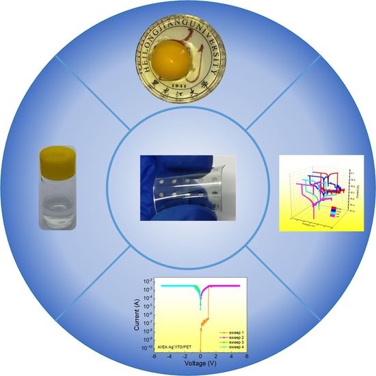
:
1. Introduction
2. Materials and Methods
2.1. Preparation of the Device
2.2. Feature Description
3. Results
3.1. Device Structure and Material Characterization
3.2. Memristor Performance
4. Conclusions
Author Contributions
Funding
Data Availability Statement
Acknowledgments
Conflicts of Interest
References
- Zoeteman, B.C.J.; Krikke, H.R.; Venselaar, J. Handling WEEE waste flows: On the effectiveness of producer responsibility in a globalizing world. Int. J. Adv. Manuf. Technol. 2009, 47, 415–436. [Google Scholar] [CrossRef]
- Mukherjee, C.; Hota, M.K.; Naskar, D.; Kundu, S.C.; Maiti, C.K. Resistive switching in natural silk fibroin protein-based bio-memristors. Phys. Status Solidi (a) 2013, 210, 1797–1805. [Google Scholar] [CrossRef]
- Ouyang, J.; Chu, C.W.; Szmanda, C.R.; Ma, L.; Yang, Y. Programmable polymer thin film and non-volatile memory device. Nat. Mater. 2004, 3, 918–922. [Google Scholar] [CrossRef]
- Wang, L.; Yang, T.; Wen, D. Tunable Multilevel Data Storage Bioresistive Random Access Memory Device Based on Egg Albumen and Carbon Nanotubes. Nanomaterials 2021, 11, 2085. [Google Scholar] [CrossRef]
- Zhu, Z.; Kin Tam, T.; Sun, F.; You, C.; Percival Zhang, Y.H. A high-energy-density sugar biobattery based on a synthetic enzymatic pathway. Nat. Commun. 2014, 5, 3026. [Google Scholar] [CrossRef]
- Chang, J.W.; Wang, C.G.; Huang, C.Y.; Tsai, T.D.; Guo, T.F.; Wen, T.C. Chicken albumen dielectrics in organic field-effect transistors. Adv. Mater. 2011, 23, 4077–4081. [Google Scholar] [CrossRef]
- Yukimoto, T.; Uemura, S.; Kamata, T.; Nakamura, K.; Kobayashi, N. Non-volatile transistor memory fabricated using DNA and eliminating influence of mobile ions on electric properties. J. Mater. Chem. 2011, 21, 15575–15579. [Google Scholar] [CrossRef]
- Waser, R.; Aono, M. Nanoionics-based resistive switching memories. Nat. Mater. 2007, 6, 833–840. [Google Scholar] [CrossRef]
- Waser, R.; Dittmann, R.; Staikov, G.; Szot, K. Redox-Based Resistive Switching Memories—Nanoionic Mechanisms, Prospects, and Challenges. Adv. Mater. 2009, 21, 2632–2663. [Google Scholar] [CrossRef]
- Kwon, D.H.; Kim, K.M.; Jang, J.H.; Jeon, J.M.; Lee, M.H.; Kim, G.H.; Li, X.S.; Park, G.S.; Lee, B.; Han, S.; et al. Atomic structure of conducting nanofilaments in TiO2 resistive switching memory. Nat. Nanotechnol. 2010, 5, 148–153. [Google Scholar] [CrossRef]
- Wang, X.F.; Tian, H.; Zhao, H.M.; Zhang, T.Y.; Mao, W.Q.; Qiao, Y.C.; Pang, Y.; Li, Y.X.; Yang, Y.; Ren, T.L. Interface Engineering with MoS2 -Pd Nanoparticles Hybrid Structure for a Low Voltage Resistive Switching Memory. Small 2018, 14, 1702525. [Google Scholar] [CrossRef] [PubMed]
- Yang, Y.; Gao, P.; Gaba, S.; Chang, T.; Pan, X.; Lu, W. Observation of conducting filament growth in nanoscale resistive memories. Nat. Commun. 2012, 3, 732. [Google Scholar] [CrossRef]
- Park, J.; Choi, J.; Chung, D.; Kim, S. Transformed Filaments by Oxygen Plasma Treatment and Improved Resistance State. Nanomaterials 2022, 12, 2716. [Google Scholar] [CrossRef]
- Shen, Z.; Zhao, C.; Qi, Y.; Xu, W.; Liu, Y.; Mitrovic, I.Z.; Yang, L.; Zhao, C. Advances of RRAM Devices: Resistive Switching Mechanisms, Materials and Bionic Synaptic Application. Nanomaterials 2020, 10, 1437. [Google Scholar] [CrossRef] [PubMed]
- Raeis-Hosseini, N.; Lee, J.S. Controlling the Resistive Switching Behavior in Starch-Based Flexible Biomemristors. ACS Appl. Mater. Int. 2016, 8, 7326–7332. [Google Scholar] [CrossRef] [PubMed]
- Hosseini, N.R.; Lee, J.S. Resistive Switching Memory Based on Bioinspired Natural Solid Polymer Electrolytes. ACS Nano 2015, 9, 419–426. [Google Scholar] [CrossRef] [PubMed]
- Ko, Y.; Kim, Y.; Baek, H.; Cho, J. Electrically Bistable Properties of Layer-by-Layer Assembled Multilayers Based on Protein Nanoparticles. ACS Nano 2011, 5, 9918–9926. [Google Scholar] [CrossRef]
- Zhang, C.; Shang, J.; Xue, W.; Tan, H.; Pan, L.; Yang, X.; Guo, S.; Hao, J.; Liu, G.; Li, R.W. Convertible resistive switching characteristics between memory switching and threshold switching in a single ferritin-based memristor. Chem. Commun. 2016, 52, 4828–4831. [Google Scholar] [CrossRef]
- Wang, Y.; Yan, X.; Dong, R. Organic memristive devices based on silver nanoparticles and DNA. Org. Electron. 2014, 15, 3476–3481. [Google Scholar] [CrossRef]
- Abbas, Y.; Dugasani, S.R.; Raza, M.T.; Jeon, Y.R.; Park, S.H.; Choi, C. The observation of resistive switching characteristics using transparent and biocompatible Cu(2+)-doped salmon DNA composite thin film. Nanotechnology 2019, 30, 335203. [Google Scholar] [CrossRef]
- Xing, Y.; Shi, C.Y.; Zhao, J.H.; Qiu, W.; Lin, N.B.; Wang, J.J.; Yan, X.B.; Yu, W.D.; Liu, X.Y. Mesoscopic-Functionalization of Silk Fibroin with Gold Nanoclusters Mediated by Keratin and Bioinspired Silk Synapse. Small 2017, 13, 1702390. [Google Scholar] [CrossRef] [PubMed]
- Shi, C.; Wang, J.; Sushko, M.L.; Qiu, W.; Yan, X.; Liu, X.Y. Silk Flexible Electronics: From Bombyx mori Silk Ag Nanoclusters Hybrid Materials to Mesoscopic Memristors and Synaptic Emulators. Adv. Funct. Mater. 2019, 29, 1904777. [Google Scholar] [CrossRef]
- Chang, Y.-C.; Jian, J.-C.; Hsu, Y.L.; Huang, W.-Y.; Young, S.-J. A Green Strategy for Developing a Self-Healing Gelatin Resistive Memory Device. ACS Appl. Polym. Mater. 2020, 2, 5318–5326. [Google Scholar] [CrossRef]
- Chang, Y.C.; Wang, Y.H. Resistive switching behavior in gelatin thin films for nonvolatile memory application. ACS Appl. Mater. Int. 2014, 6, 5413–5421. [Google Scholar] [CrossRef]
- Ge, L.; Xuan, W.; Liu, S.; Huang, S.; Wang, X.; Dong, S.; Jin, H.; Luo, J. Biomaterial Gelatin Film Based Crossbar Structure Resistive Switching Devices. IEEE Trans. Nanotechnol. 2018, 17, 78–83. [Google Scholar] [CrossRef]
- Liu, D.; Jing, Q.; Cheng, H. Synaptic-functional and fully water-soluble transient memristor made from materials compatible with semiconductor technology. Jpn. J. Appl. Phys. 2019, 58, 060903. [Google Scholar] [CrossRef]
- Koduvayur Ganeshan, S.; Selamneni, V.; Sahatiya, P. Water dissolvable MoS2 quantum dots/PVA film as an active material for destructible memristors. New J. Chem. 2020, 44, 11941–11948. [Google Scholar] [CrossRef]
- Guo, Y.; Hu, W.; Zeng, F.; Zhang, C.; Peng, Y.; Guo, Y. Ultrafast degradable resistive switching memory based on α-lactose thin films. Org. Electron. 2020, 83, 105750. [Google Scholar] [CrossRef]
- Lin, N.; Hu, F.; Sun, Y.; Wu, C.; Xu, H.; Liu, X.Y. Construction of White-Light-Emitting Silk Protein Hybrid Films by Molecular Recognized Assembly among Hierarchical Structures. Adv. Funct. Mater. 2014, 24, 5284–5290. [Google Scholar] [CrossRef]
- Bae, H.; Lee, B.H.; Lee, D.; Seol, M.L.; Kim, D.; Han, J.W.; Kim, C.K.; Jeon, S.B.; Ahn, D.; Park, S.J.; et al. Physically Transient Memory on a Rapidly Dissoluble Paper for Security Application. Sci. Rep. 2016, 6, 38324. [Google Scholar] [CrossRef] [Green Version]
- Ji, X.; Song, L.; Zhong, S.; Jiang, Y.; Lim, K.G.; Wang, C.; Zhao, R. Biodegradable and Flexible Resistive Memory for Transient Electronics. J. Phys. Chem. 2018, 122, 16909–16915. [Google Scholar] [CrossRef]
- Huang, W.-Y.; Chang, Y.-C.; Sie, Y.-F.; Yu, C.-R.; Wu, C.-Y.; Hsu, Y.-L. Bio-Cellulose Substrate for Fabricating Fully Biodegradable Resistive Random Access Devices. ACS Appl. Polym. Mater. 2021, 3, 4478–4484. [Google Scholar] [CrossRef]
- Chen, Y.-C.; Su, Y.-K.; Huang, C.-Y.; Yu, H.-C.; Cheng, C.-Y.; Chang, T.-H. Bistable Resistive Switching Characteristics of Poly(2-hydroxyethyl methacrylate) Thin Film Memory Devices. Appl. Phys. Express 2011, 4, 054204. [Google Scholar] [CrossRef]
- Zhang, J.; Yang, H.; Zhang, Q.-l.; Dong, S.; Luo, J.K. Bipolar resistive switching characteristics of low temperature grown ZnO thin films by plasma-enhanced atomic layer deposition. Appl. Phys. Lett. 2013, 102, 012113. [Google Scholar] [CrossRef]
- Zhuge, F.; Dai, W.; He, C.L.; Wang, A.Y.; Liu, Y.W.; Li, M.; Wu, Y.H.; Cui, P.; Li, R.-W. Nonvolatile resistive switching memory based on amorphous carbon. Appl. Phys. Lett. 2010, 96, 163505. [Google Scholar] [CrossRef]


Publisher’s Note: MDPI stays neutral with regard to jurisdictional claims in published maps and institutional affiliations. |
© 2022 by the authors. Licensee MDPI, Basel, Switzerland. This article is an open access article distributed under the terms and conditions of the Creative Commons Attribution (CC BY) license (https://creativecommons.org/licenses/by/4.0/).
Share and Cite
Wang, L.; Zhang, Y.; Zhang, P.; Wen, D. Physically Transient, Flexible, and Resistive Random Access Memory Based on Silver Ions and Egg Albumen Composites. Nanomaterials 2022, 12, 3061. https://doi.org/10.3390/nano12173061
Wang L, Zhang Y, Zhang P, Wen D. Physically Transient, Flexible, and Resistive Random Access Memory Based on Silver Ions and Egg Albumen Composites. Nanomaterials. 2022; 12(17):3061. https://doi.org/10.3390/nano12173061
Chicago/Turabian StyleWang, Lu, Yukai Zhang, Peng Zhang, and Dianzhong Wen. 2022. "Physically Transient, Flexible, and Resistive Random Access Memory Based on Silver Ions and Egg Albumen Composites" Nanomaterials 12, no. 17: 3061. https://doi.org/10.3390/nano12173061