
Nanoparticle/Core-Shell Composite Structures with Superior Optical and Electrochemical Properties in a Dye-Sensitized Solar Cell
 ,
,
Abstract
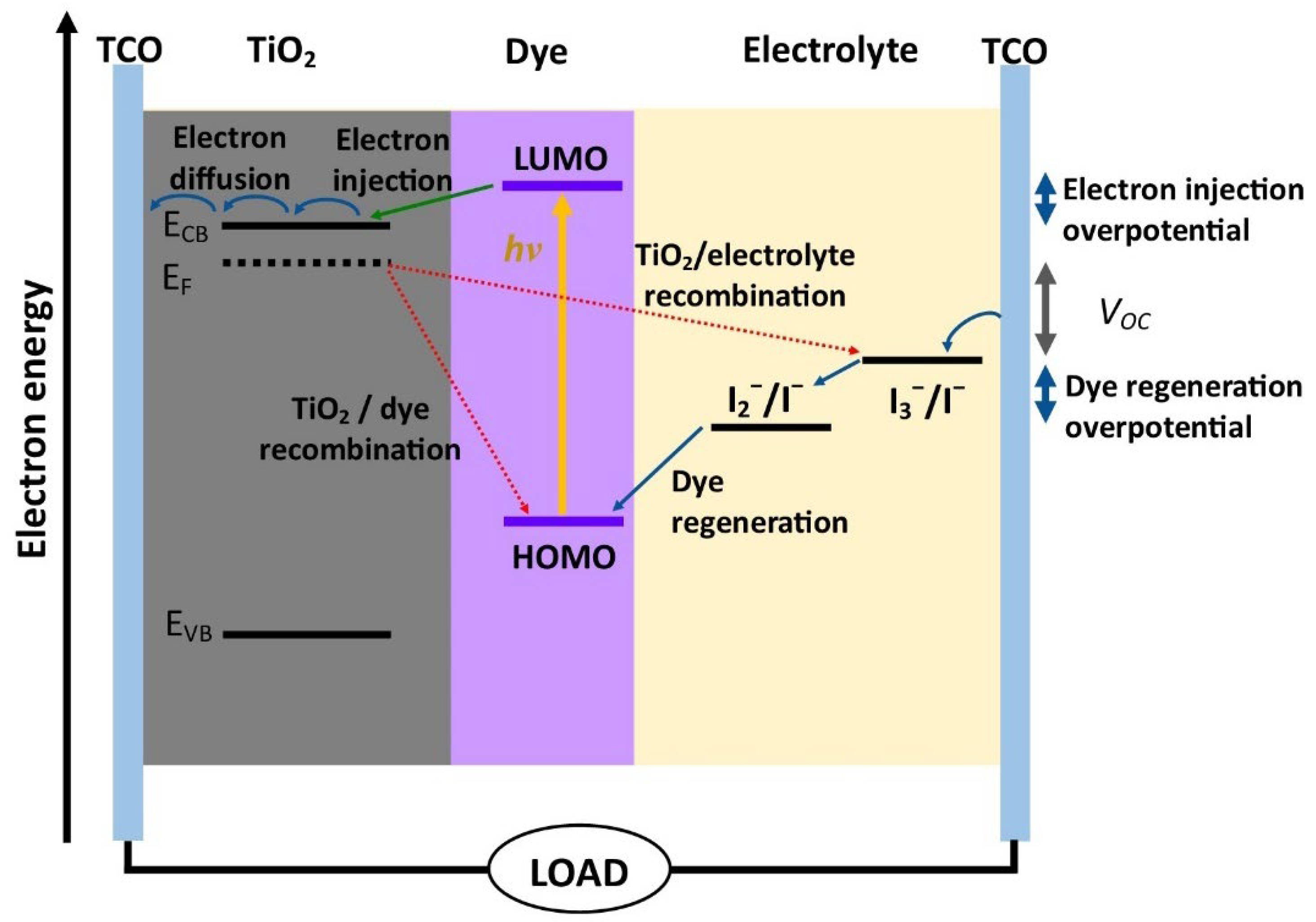
:1. Introduction
2. Materials and Methods
2.1. Synthesis of TiO2 Nanoparticles
2.2. Synthesis of SiO2-TiO2 Core-Shell Structures
2.3. Fabrication of DSSC
2.4. Samples Characterization and Performance Verification
3. Results and Discussion
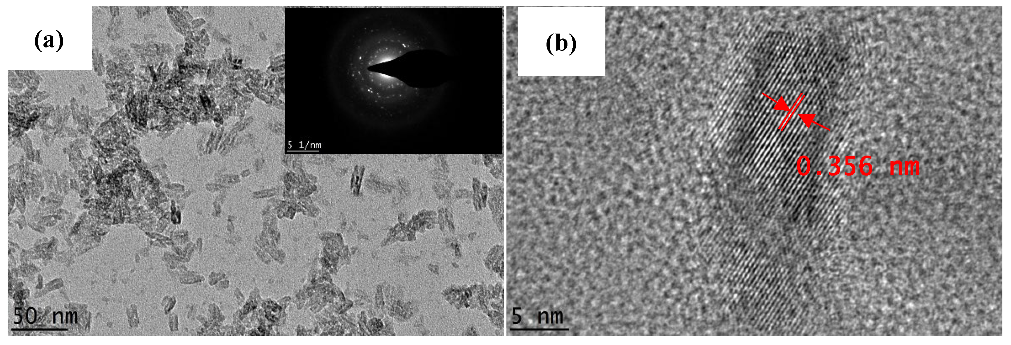
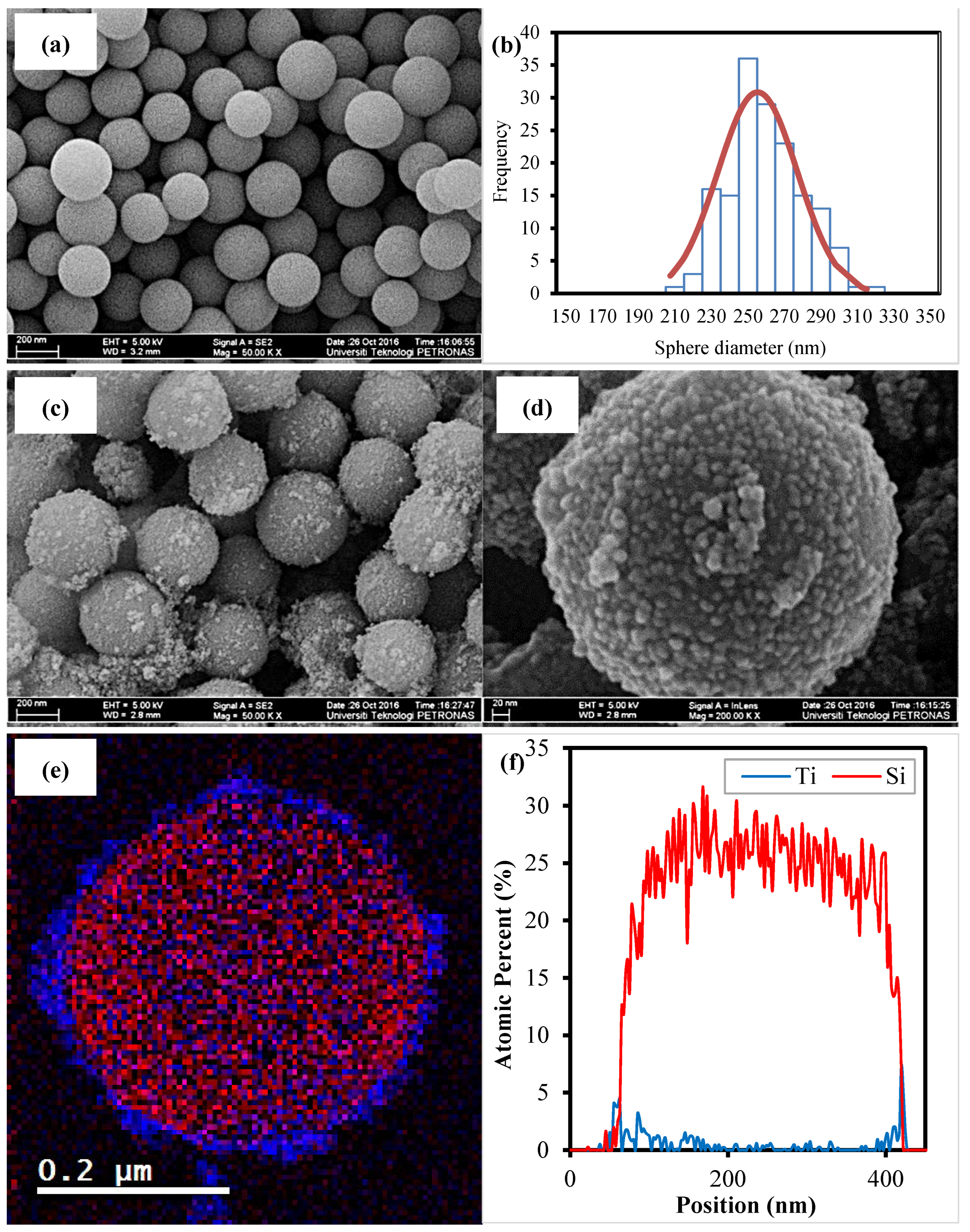
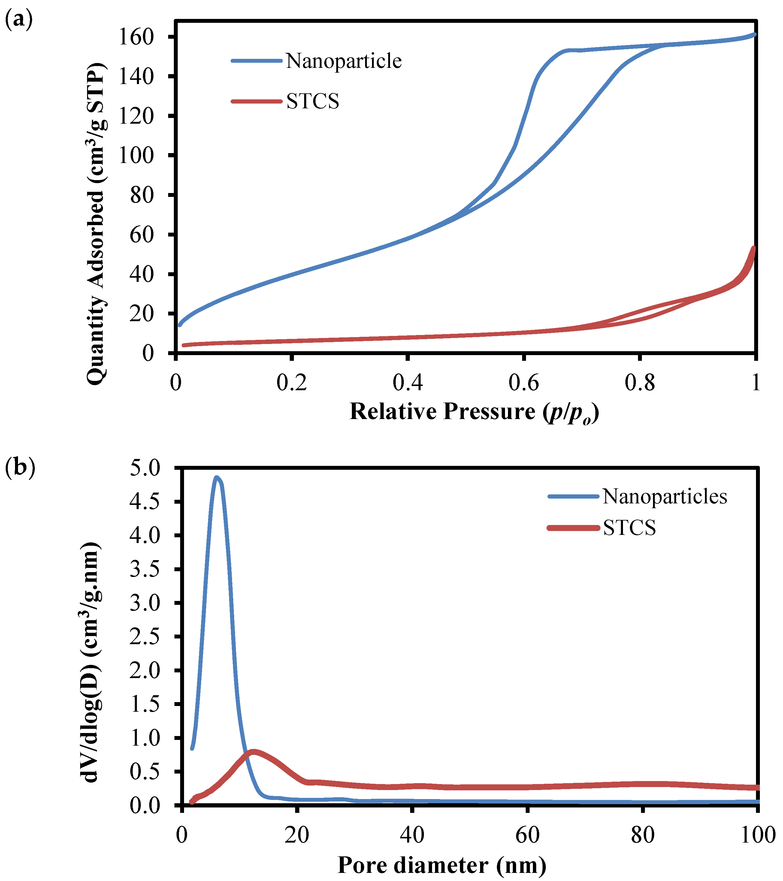
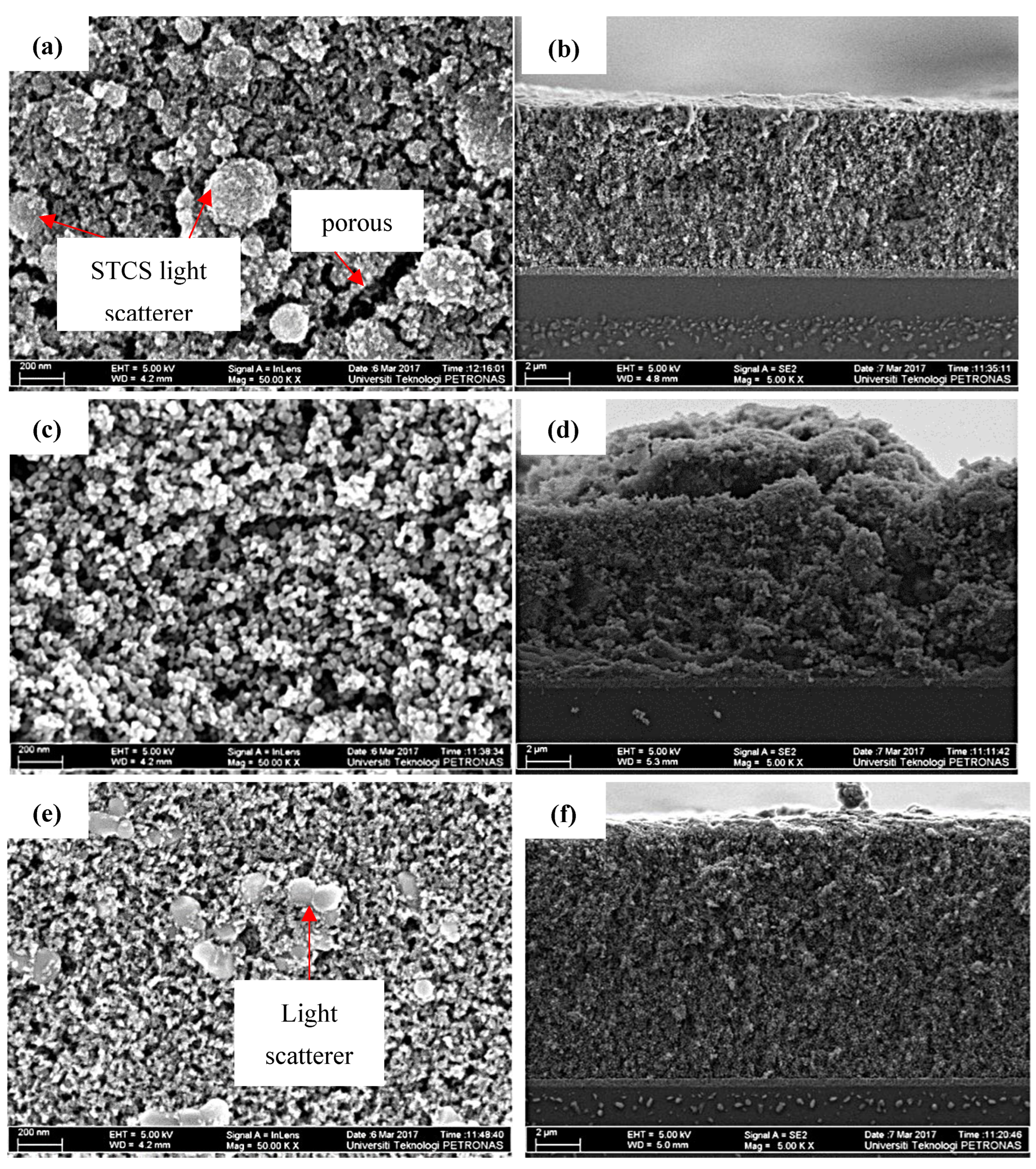
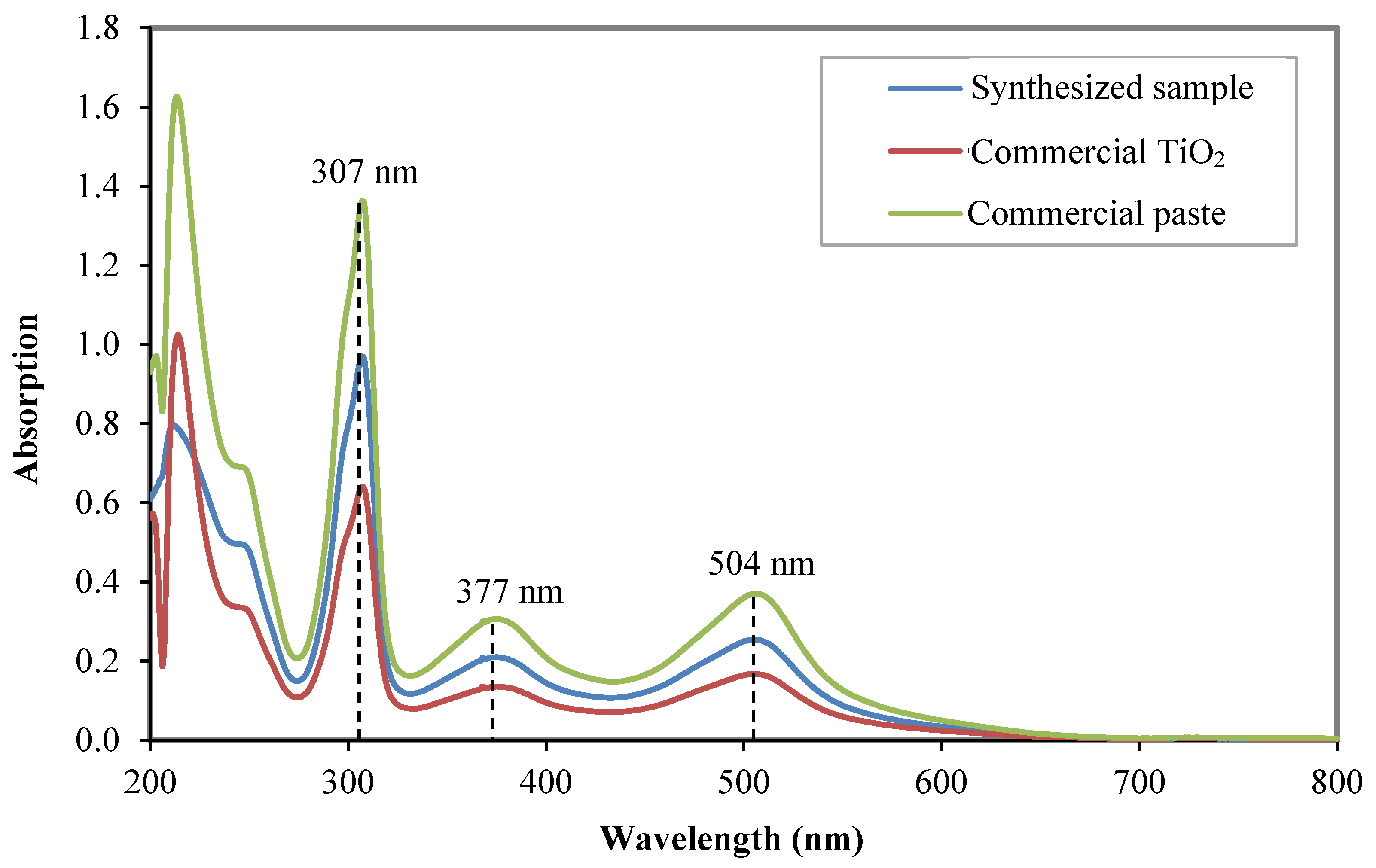
3.1. Physical Properties of the Synthesized Samples
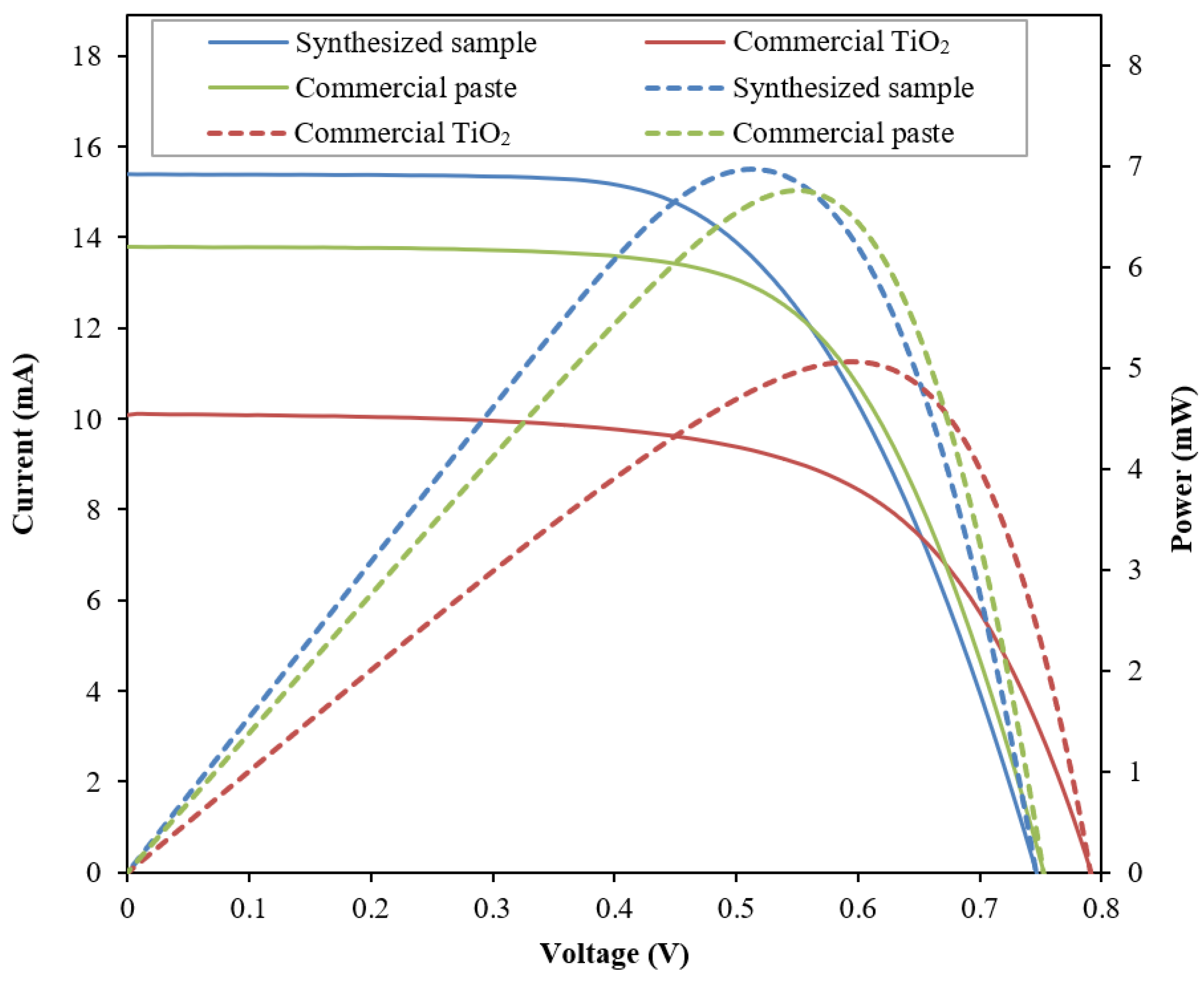
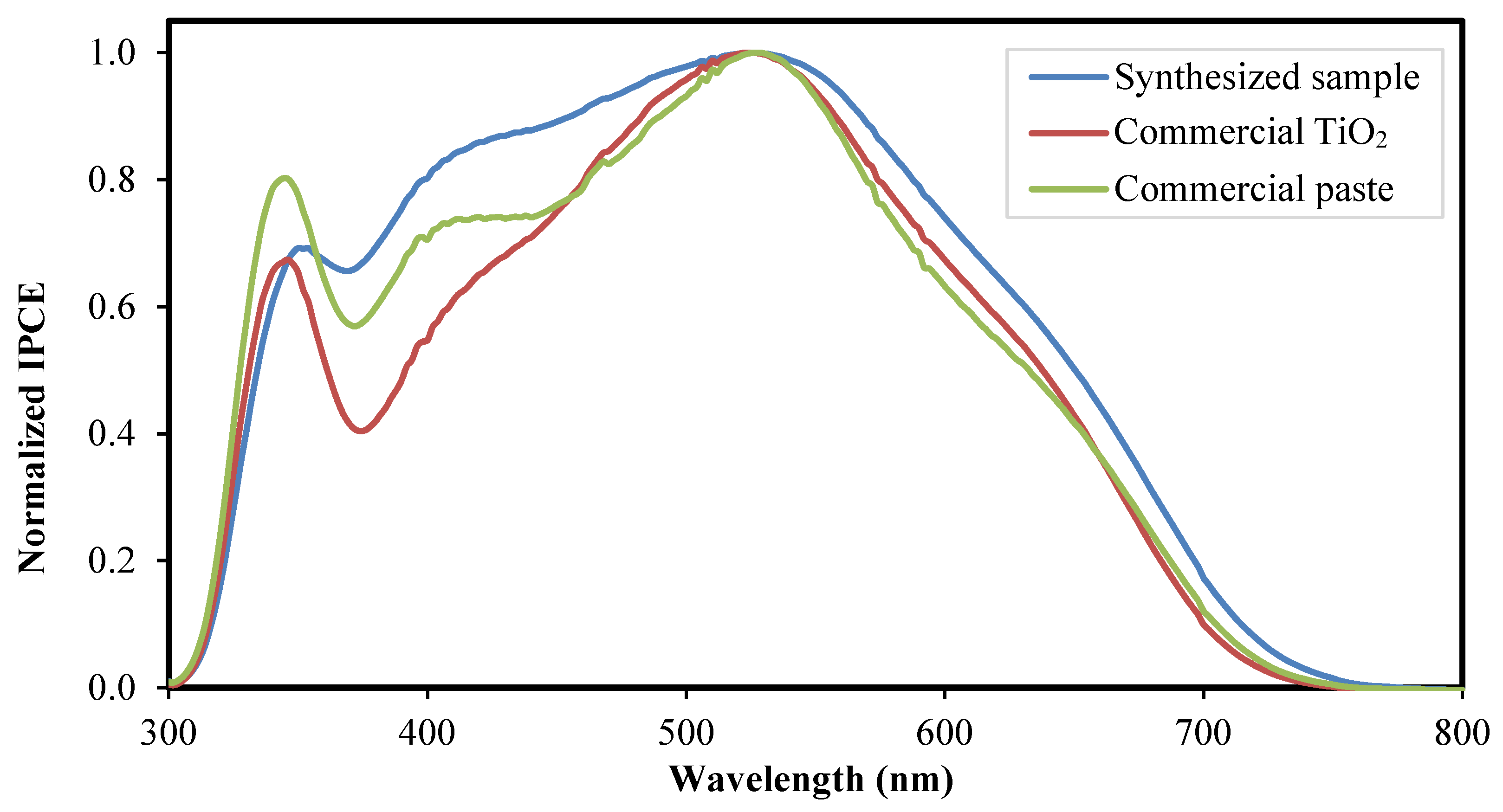
3.2. Performance Analysis of Fabricated DSSC
4. Conclusions
Author Contributions
Funding
Data Availability Statement
Acknowledgments
Conflicts of Interest
References
- Lee, H.M.; Yoon, J.H. Power performance analysis of a transparent DSSC BIPV window based on 2 year measurement data in a full-scale mock-up. Appl. Energy 2018, 225, 1013–1021. [Google Scholar] [CrossRef]
- Chung, M.H.; Park, B.R.; Choi, E.J.; Choi, Y.J.; Lee, C.; Hong, J.; Cho, H.U.; Cho, J.H.; Moon, J.W. Performance level criteria for semi-transparent photovoltaic windows based on dye-sensitized solar cells. Sol. Energy Mater. Sol. Cells 2020, 217, 110683. [Google Scholar] [CrossRef]
- Aslam, A.; Mehmood, U.; Arshad, M.H.; Ishfaq, A.; Zaheer, J.; Ul Haq Khan, A.; Sufyan, M. Dye-sensitized solar cells (DSSCs) as a potential photovoltaic technology for the self-powered internet of things (IoTs) applications. Sol. Energy 2020, 207, 874–892. [Google Scholar] [CrossRef]
- Devadiga, D.; Selvakumar, M.; Shetty, P.; Santosh, M.S. The integration of flexible dye-sensitized solar cells and storage devices towards wearable self-charging power systems: A review. Renew. Sustain. Energy Rev. 2022, 159, 112252. [Google Scholar] [CrossRef]
- Nazeeruddin, M.K.; Baranoff, E.; Grätzel, M. Dye-sensitized solar cells: A brief overview. Sol. Energy 2011, 85, 1172–1178. [Google Scholar] [CrossRef]
- Gong, J.; Sumathy, K.; Qiao, Q.; Zhou, Z. Review on dye-sensitized solar cells (DSSCs): Advanced techniques and research trends. Renew. Sustain. Energy Rev. 2017, 68, 234–246. [Google Scholar] [CrossRef]
- Lau, K.K.S.; Soroush, M. Overview of dye-sensitized solar cells. In Dye-Sensitized Solar Cells; Soroush, M., Lau, K.K.S., Eds.; Academic Press: Cambridge, MA, USA, 2019; pp. 1–49. [Google Scholar] [CrossRef]
- Zhang, Q.; Dandeneau, C.S.; Park, K.; Liu, D.; Zhou, X.; Jeong, Y.-H.; Cao, G. Light scattering with oxide nanocrystallite aggregates for dyesensitized solar cell application. J. Nanophotonics 2010, 4, 041540. [Google Scholar] [CrossRef]
- Hagfeldt, A.; Boschloo, G.; Sun, L.; Kloo, L.; Pettersson, H. Dye-sensitized solar cells. Chem. Rev. 2010, 110, 6595–6663. [Google Scholar] [CrossRef]
- Shalini, S.; Balasundaraprabhu, R.; Prasanna, S.; Mallick, T.K.; Senthilarasu, S. Review on natural dye sensitized solar cells: Operation, materials and methods. Renew. Sustain. Energy Rev. 2015, 51, 1306–1325. [Google Scholar] [CrossRef]
- Son, Y.J.; Kang, J.S.; Yoon, J.; Kim, J.; Jeong, J.; Kang, J.; Lee, M.J.; Park, H.S.; Sung, Y.-E. Influence of TiO2 particle size on dye-sensitized solar cells employing an organic sensitizer and a cobalt(III/II) redox electrolyte. J. Phys. Chem. C 2018, 122, 7051–7060. [Google Scholar] [CrossRef]
- Kang, M.G.; Ryu, K.S.; Chang, S.H.; Park, N.G.; Hong, J.S.; Kim, K.-J. Dependence of TiO2 film thickness on photocurrent-voltage characteristics of dye-sensitized solar cells. Bull.-Korean Chem. Soc. 2004, 25, 742–744. [Google Scholar]
- Shah, S.K.; Ishaq, M.; Khattak, S.A.; Ullah, I.; Hayat, K.; Khan, M.; Khan, G.; Tabbasam, L. Effect of mesoporous TiO2 thicknesses on the performance of solid-state dye-sensitized solar cells. J. Electron. Mater. 2019, 48, 696–704. [Google Scholar] [CrossRef]
- Zhang, Q.; Chou, T.P.; Russo, B.; Jenekhe, S.A.; Cao, G. Polydisperse aggregates of ZnO nanocrystallites: A method for energy-conversion-efficiency enhancement in dye-sensitized solar cells. Adv. Funct. Mater. 2008, 18, 1654–1660. [Google Scholar]
- Zhao, F.; Ma, R.; Jiang, Y. Strong efficiency improvement in dye-sensitized solar cells by novel multi-dimensional TiO2 photoelectrode. Appl. Surf. Sci. 2018, 434, 11–15. [Google Scholar] [CrossRef]
- Mohammadian-Sarcheshmeh, H.; Arazi, R.; Mazloum-Ardakani, M. Application of bifunctional photoanode materials in DSSCs: A review. Renew. Sustain. Energy Rev. 2020, 134, 110249. [Google Scholar] [CrossRef]
- Mustafa, M.N.; Sulaiman, Y. Review on the effect of compact layers and light scattering layers on the enhancement of dye-sensitized solar cells. Sol. Energy 2021, 215, 26–43. [Google Scholar] [CrossRef]
- Chou, T.P.; Zhang, Q.; Fryxell, G.E.; Cao, G. Hierarchically structured ZnO film for dye-sensitized solar cells with enhanced energy conversion efficiency. Adv. Mater. 2007, 19, 2588–2592. [Google Scholar] [CrossRef]
- Jiu, J.; Isoda, S.; Adachi, M.; Wang, F. Preparation of TiO2 nanocrystalline with 3–5nm and application for dye-sensitized solar cell. J. Photochem. Photobiol. A Chem. 2007, 189, 314–321. [Google Scholar] [CrossRef]
- Jiu, J.; Isoda, S.; Adachi, M.; Wang, H. Dye-sensitized solar cell based on nanocrystalline TiO2 with 3–10 nm in diameter. J. Mater. Sci. Mater. Electron. 2007, 18, 593–597. [Google Scholar] [CrossRef]
- Chou, T.P.; Zhang, Q.; Russo, B.; Fryxell, G.E.; Cao, G. Titania particle size effect on the overall performance of dye-sensitized solar cells. J. Phys. Chem. C 2007, 111, 6296–6302. [Google Scholar] [CrossRef]
- Karim, N.A.; Mehmood, U.; Zahid, H.F.; Asif, T. Nanostructured photoanode and counter electrode materials for efficient dye-sensitized solar cells (DSSCs). Sol. Energy 2019, 185, 165–188. [Google Scholar] [CrossRef]
- Wang, Y.; Chen, E.; Lai, H.; Lu, B.; Hu, Z.; Qin, X.; Shi, W.; Du, G. Enhanced light scattering and photovoltaic performance for dye-sensitized solar cells by embedding submicron SiO2/TiO2 core/shell particles in photoanode. Ceram. Int. 2013, 39, 5407–5413. [Google Scholar] [CrossRef]
- Falahatdoost, S.; Ara, M.H.M.; Shaban, Z.; Ghazyani, N. Optical investigation of shell thickness in light scattering SiO2 particle with TiO2 nanoshells and its application in dye sensitized solar cells. Opt. Mater. 2015, 47, 51–55. [Google Scholar] [CrossRef]
- Son, S.; Hwang, S.H.; Kim, C.; Yun, J.Y.; Jang, J. Designed synthesis of SiO2/TiO2 core/shell structure as light scattering material for highly efficient dye-sensitized solar cells. ACS Appl. Mater. Interfaces 2013, 5, 4815–4820. [Google Scholar] [CrossRef]
- Lee, J.-W.; Kong, S.; Kim, W.-S.; Kim, J. Preparation and characterization of SiO2/TiO2 core-shell particles with controlled shell thickness. Mater. Chem. Phys. 2007, 106, 39–44. [Google Scholar]
- Tong, H.; Enomoto, N.; Inada, M.; Tanaka, Y.; Hojo, J. Hydrothermal synthesis of mesoporous TiO2-SiO2 core-shell composites for dye-sensitized solar cells. Electrochim. Acta 2014, 130, 329–334. [Google Scholar] [CrossRef]
- Ullah, S.; Ferreira-Neto, E.P.; Pasa, A.A.; Alcântara, C.C.J.; Acuña, J.J.S.; Bilmes, S.A.; Martínez Ricci, M.L.; Landers, R.; Fermino, T.Z.; Rodrigues-Filho, U.P. Enhanced photocatalytic properties of core@shell SiO2@TiO2 nanoparticles. Appl. Catal. B Environ. 2015, 179, 333–343. [Google Scholar] [CrossRef]
- Zaine, S.N.A.; Mohamed, N.M.; Khatani, M.; Samsudin, A.E.; Shahid, M.U. Improving the light scattering efficiency of photoelectrode dye-sensitized solar cell through optimization of core-shell structure. Mater. Today Commun. 2019, 19, 220–229. [Google Scholar] [CrossRef]
- Shahid, M.U.; Mohamed, N.M.; Muhsan, A.S.; Zaine, S.N.A.; Bashiri, R.; Khatani, M.; Samsudin, A.E. Solvent exfoliated graphene incorporated mixed phase TiO2 transparent photoelectrode for the efficient and color transparent dye-sensitized solar cell. Sol. Energy 2020, 206, 317–329. [Google Scholar] [CrossRef]
- Zaine, S.N.A.; Mohamed, N.M.; Khatani, M.; Samsudin, A.E.; Shahid, M.U. Trap state and charge recombination in nanocrystalline passivized conductive and photoelectrode interface of dye-sensitized solar cell. Coatings 2020, 10, 284. [Google Scholar] [CrossRef]
- Johari, N.D.; Rosli, Z.M.; Juoi, J.M.; Yazid, S.A. Comparison on the TiO2 crystalline phases deposited via dip and spin coating using green sol–gel route. J. Mater. Res. Technol. 2019, 8, 2350–2358. [Google Scholar] [CrossRef]
- Deng, H.; Zeng, Y.; Ishaq, M.; Yuan, S.; Zhang, H.; Yang, X.; Hou, M.; Farooq, U.; Huang, J.; Sun, K.; et al. Quasiepitaxy strategy for efficient full-inorganic Sb2S3 solar cells. Adv. Funct. Mater. 2019, 29, 1901720. [Google Scholar] [CrossRef]
- Agarwala, S.; Kevin, M.; Wong, A.S.W.; Peh, C.K.N.; Thavasi, V.; Ho, G.W. Mesophase ordering of TiO2 film with high surface area and strong light harvesting for dye-sensitized solar cell. ACS Appl. Mater. Interfaces 2010, 2, 1844–1850. [Google Scholar] [CrossRef] [PubMed]
- Zhang, S.; Yang, X.; Numata, Y.; Han, L. Highly efficient dye-sensitized solar cells: Progress and future challenges. Energy Environ. Sci. 2013, 6, 1443–1464. [Google Scholar]
- Zhang, Q.; Myers, D.; Lan, J.; Jenekhe, S.A.; Cao, G. Applications of light scattering in dye-sensitized solar cells. Phys. Chem. Chem. Phys. 2012, 14, 14982–14998. [Google Scholar] [CrossRef] [PubMed]
- Bohren, C.F.; Huffman, D.R. Appendix B: Coated sphere. In Absorption and Scattering of Light by Small Particles; Wiley: New York, NY, USA, 2007; pp. 483–489. [Google Scholar] [CrossRef]
- Adachi, M.; Sakamoto, M.; Jiu, J.; Ogata, Y.; Isoda, S. Determination of parameters of electron transport in dye-sensitized solar cells using electrochemical impedance spectroscopy. J. Phys. Chem. B 2006, 110, 13872–13880. [Google Scholar] [CrossRef]
- Bisquert, J. Theory of the impedance of charge transfer via surface states in dye-sensitized solar cells. J. Electroanal. Chem. 2010, 646, 43–51. [Google Scholar] [CrossRef]


| Sample | Intensity (Count) | FWHM (β) | d-Spacing (Å) | Crystallite Size (nm) |
|---|---|---|---|---|
| Synthesized sample | 2374.32 | 0.8253 | 3.5181 | 9.8 |
| Commercial TiO2 | 4750.41 | 0.4529 | 3.5200 | 17.6 |
| Commercial paste | 4048.55 | 0.4767 | 3.5183 | 14.9 |
| Sample | Jsc (mA/cm2) | Voc (V) | FF | η (%) | Pmax (mW) |
|---|---|---|---|---|---|
| Synthesized sample | 15.144 ± 0.33 | 0.747 ± 0.001 | 0.608 ± 0.003 | 6.880 ± 0.124 | 6.880 ± 0.124 |
| Commercial TiO2 | 10.525 ± 0.386 | 0.793 ± 0.018 | 0.641 ± 0.013 | 5.289 ± 0.197 | 5.289 ± 0.197 |
| Commercial paste | 13.534 ± 0.353 | 0.753 ± 0.007 | 0.655 ± 0.004 | 6.626 ± 0.134 | 6.626 ± 0.134 |
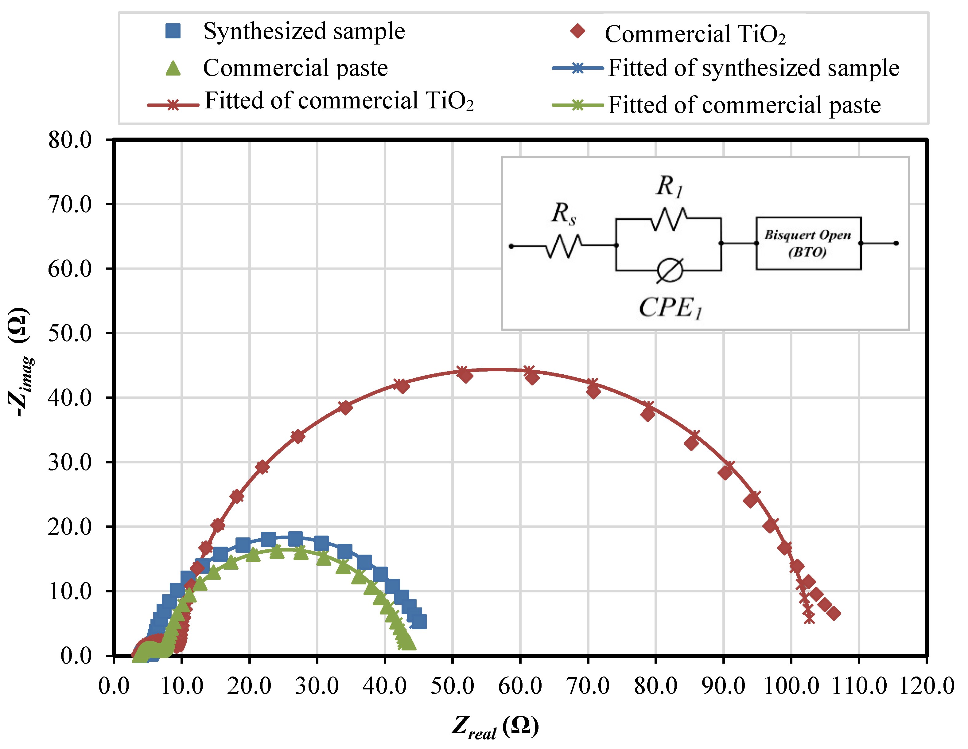
| Sample | Rt (Ω) | Rbr (Ω) | Cµ (µF) | τn (s) | k (s−1) | Dn (cm2 s−1) | Ln (µm) | Con (Ωcm s−1) | ns (cm−3) |
|---|---|---|---|---|---|---|---|---|---|
| Synthesized sample | 1.20 | 39.93 | 5.39 × 10⁻³ | 0.215 | 4.650 | 1.55 × 10⁻⁶ | 5.766 | 0.1485 | 10.80 × 10¹⁷ |
| Commercial TiO2 | 3.66 | 93.80 | 1.10 × 10⁻³ | 0.103 | 9.718 | 2.49 × 10⁻⁶ | 5.062 | 1.00483 | 1.53 × 10¹⁷ |
| Commercial paste | 4.78 | 35.25 | 2.34 × 10⁻³ | 0.082 | 12.133 | 0.89 × 10⁻⁶ | 2.714 | 0.4919 | 3.26 × 10¹⁷ |
Publisher’s Note: MDPI stays neutral with regard to jurisdictional claims in published maps and institutional affiliations. |
© 2022 by the authors. Licensee MDPI, Basel, Switzerland. This article is an open access article distributed under the terms and conditions of the Creative Commons Attribution (CC BY) license (https://creativecommons.org/licenses/by/4.0/).
Share and Cite
Zaine, S.N.A.; Mohamed, N.M.; Khatani, M.; Shahid, M.U. Nanoparticle/Core-Shell Composite Structures with Superior Optical and Electrochemical Properties in a Dye-Sensitized Solar Cell. Nanomaterials 2022, 12, 3128. https://doi.org/10.3390/nano12183128
Zaine SNA, Mohamed NM, Khatani M, Shahid MU. Nanoparticle/Core-Shell Composite Structures with Superior Optical and Electrochemical Properties in a Dye-Sensitized Solar Cell. Nanomaterials. 2022; 12(18):3128. https://doi.org/10.3390/nano12183128
Chicago/Turabian StyleZaine, Siti Nur Azella, Norani Muti Mohamed, Mehboob Khatani, and Muhammad Umair Shahid. 2022. "Nanoparticle/Core-Shell Composite Structures with Superior Optical and Electrochemical Properties in a Dye-Sensitized Solar Cell" Nanomaterials 12, no. 18: 3128. https://doi.org/10.3390/nano12183128