
Spatially-Localized Functionalization on Nanostructured Surfaces for Enhanced Plasmonic Sensing Efficacy
 , , , and
Abstract
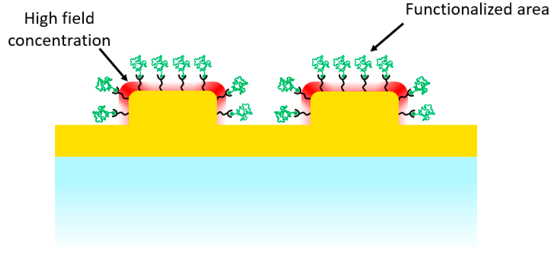
:1. Introduction
2. Materials and Methods
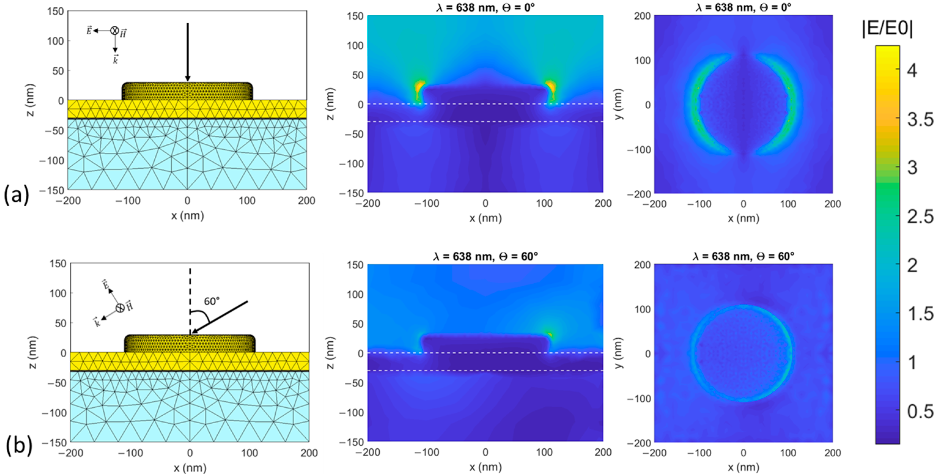
2.1. Numerical Modeling of Nanodisks Arrays
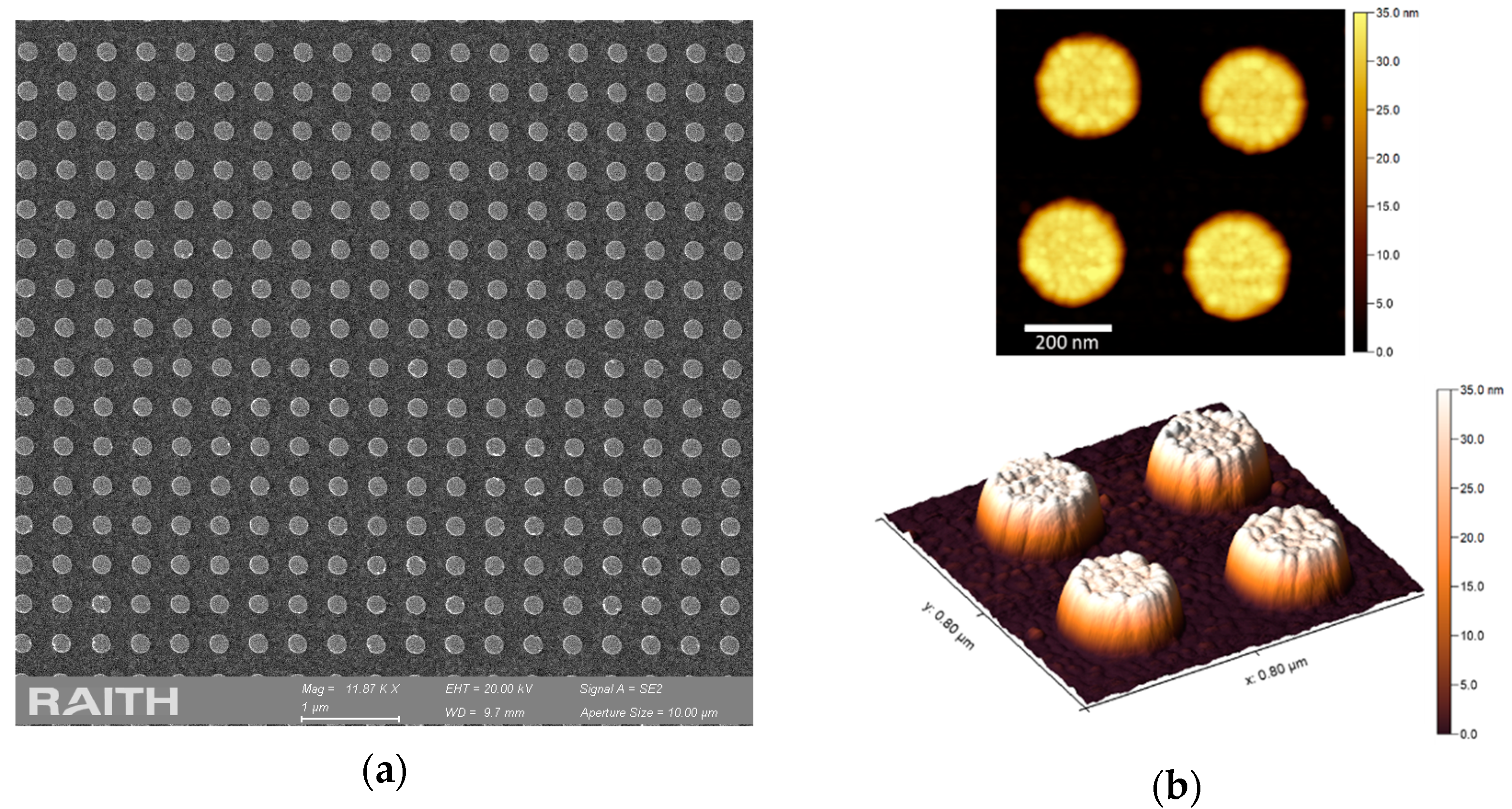
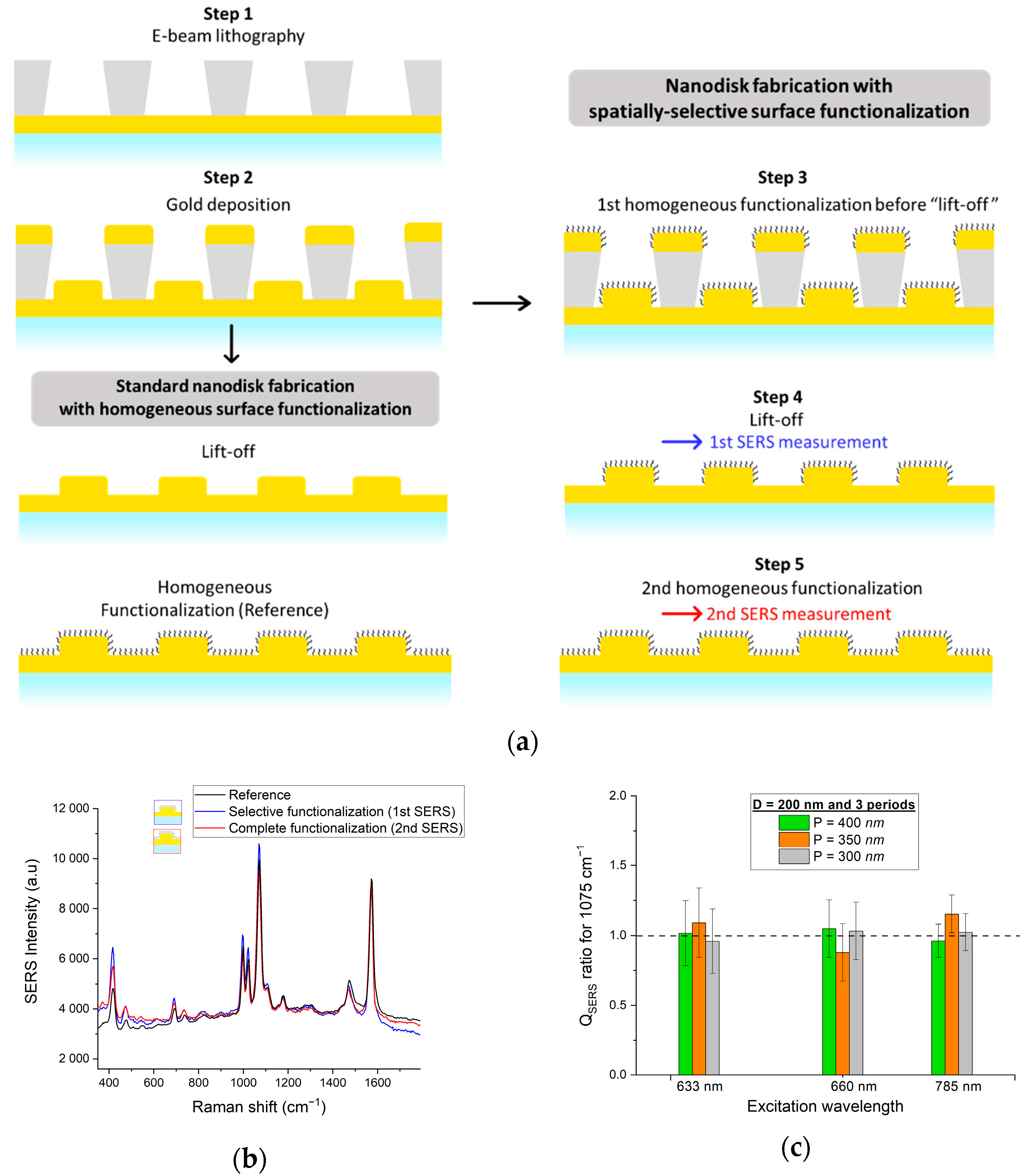
2.2. Fabrication of Nanodisks Arrays
2.3. Surface Functionalization with Thiophenol
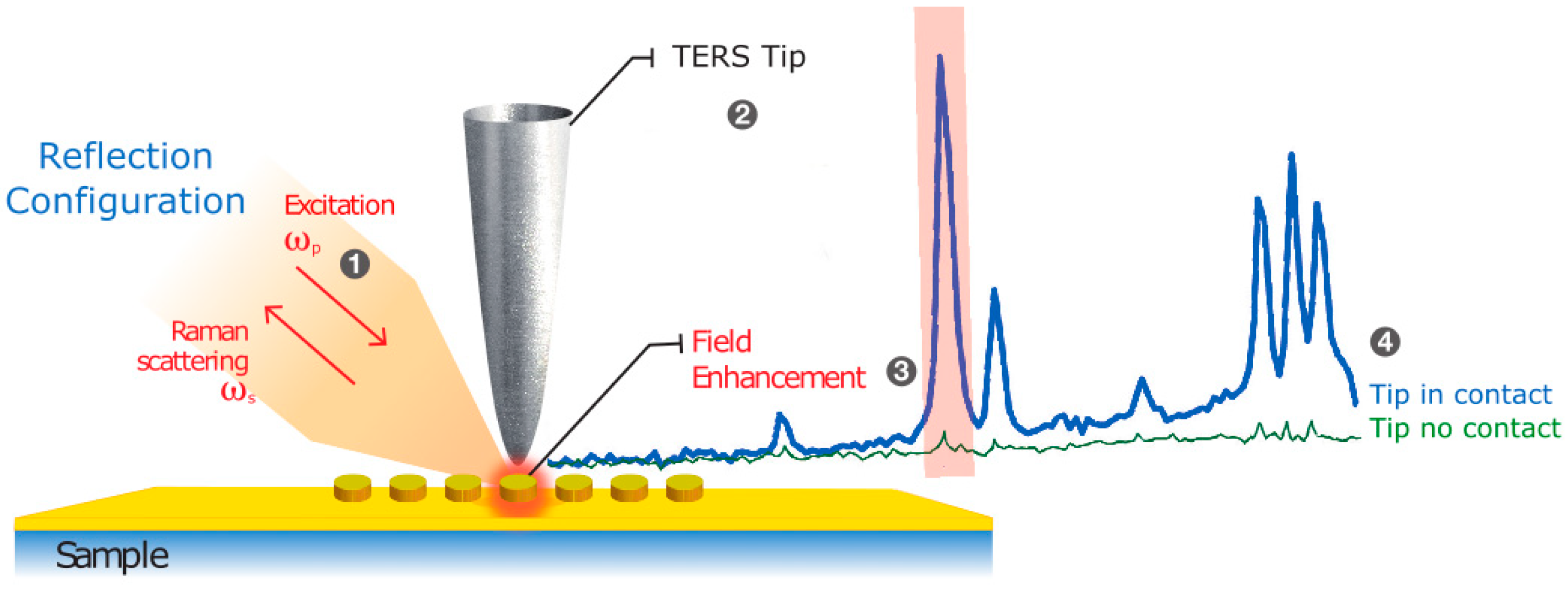
2.4. TERS and SERS Measurement Methodology
3. Results and Discussion
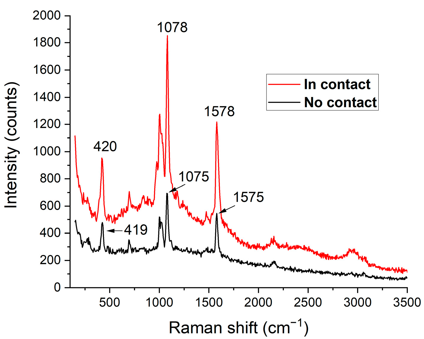
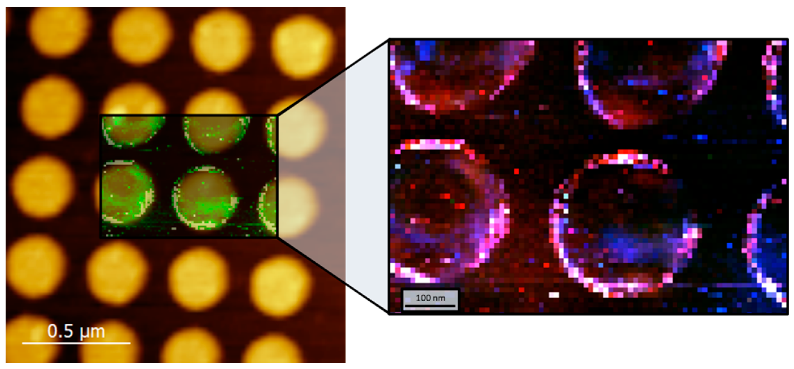
3.1. TERS and SERS Measurements on Samples with Homogeneous Surface Functionalization
3.2. SERS Measurements on Samples with Spatially-Localized Surface Functionalization
4. Conclusions
Supplementary Materials
Author Contributions
Funding
Institutional Review Board Statement
Informed Consent Statement
Data Availability Statement
Conflicts of Interest
References
- Le Ru, E.; Etchegoin, P. Principles of Surface-Enhanced Raman Spectroscopy; Elsevier: Amsterdam, The Netherlands, 2008. [Google Scholar] [CrossRef]
- Bryche, J.-F.; Gillibert, R.; Barbillon, G.; Gogol, P.; Moreau, J.; Lamy de la Chapelle, M.; Bartenlian, B.; Canva, M. Plasmonic En-hancement by a Continuous Gold Underlayer: Application to SERS Sensing. Plasmonic 2015, 11, 601–698. [Google Scholar] [CrossRef]
- Mandal, P.; Tewari, B.S. Progress in surface enhanced Raman scattering molecular sensing: A review. Surf. Interfaces 2022, 28, 101655. [Google Scholar] [CrossRef]
- Jia, K.; Adam, P.M.; Marks, R.S.; Ionescu, R.E. Fixed Escherichia coli bacterial templates enable the production of sensitive SERS-based gold nanostructures. Sens. Actuators B Chem. 2015, 211, 213–219. [Google Scholar] [CrossRef]
- Le Ru, E.C.; Myer, M.; Etchegoin, P.G. Proof of Single-Molecule Sensitivity in Surface Enhanced Raman Scattering (SERS) by Means of a Two-Analyte Technique. J. Phys. Chem. B 2006, 110, 1944–2948. [Google Scholar] [CrossRef] [PubMed]
- Yue, W.; Gong, T.; Long, X.; Kravets, V.; Gao, P.; Pu, M.; Wang, C. Sensitive and reproducible surface-enhanced raman spectroscopy (SERS) with arrays of dimer-nanopillars. Sens. Actuators B Chem. 2020, 322, 128563. [Google Scholar] [CrossRef]
- Yue, W.; Yang, Y.; Wang, Z.; Chen, L.; Wang, X. Surface-enhanced Raman scattering on gold nanorod pairs with interconnec-tion bars of different widths. Sens. Actuators B Chem. 2012, 171–172, 734–738. [Google Scholar] [CrossRef]
- Bryche, J.-F.; Gillibert, R.; Barbillon, G.; Sarkar, M.; Coutrot, A.-L.; Hamouda, F.; Aassime, A.; Moreau, J.; Lamy de la Chapelle, M.; Bartenlian, B.; et al. Density effect of gold nanodisks on the SERS intensity for a highly sensitive detection of chemical molecules. J. Mater Sci. 2015, 50, 6601–6607. [Google Scholar] [CrossRef] [Green Version]
- Bryche, J.-F.; Hamouda, F.; Besbes, M.; Gogol, P.; Moreau, J.; Lamy de la Chapelle, M.; Canva, M.; Bartenlian, B. Experimental and numerical investigation of biosensors plasmonic substrates induced differences by e-beam, soft and hard UV-NIL fabrication techniques. Micro Nano Eng. 2019, 2, 122–130. [Google Scholar] [CrossRef]
- Banville, F.A.; Moreau, J.; Chabot, K.; Cattoni, A.; Fröhlich, U.; Bryche, J.-F.; Collin, S.; Charette, P.G.; Grandbois, M.; Canva, M. Nanoplasmonics-enhanced label-free imaging of endothelial cell monolayer integrity. Biosens. Bioelectron. 2019, 141, 111478. [Google Scholar] [CrossRef] [PubMed]
- Sarkar, M.; Besbes, M.; Moreau, J.; Bryche, J.F.; Olivéro, A.; Barbillon, G.; Coutrot, A.L.; Bartenlian, B.; Canva, M. Hybrid Plas-monic Mode by Resonant Coupling of Localized Plasmons to Propagating Plasmons in a Kretschmann Configuration. ACS Pho-Tonics 2015, 2, 237–245. [Google Scholar] [CrossRef]
- Bryche, J.F.; Tsigara, A.; Bélier, B.; de la Chapelle, M.L.; Canva, M.; Bartenlian, B.; Barbillon, G. Surface enhanced Raman scattering improvement of gold triangular nanoprisms by a gold reflective underlayer for chemical sensing. Sens. Actuators B Chem. 2016, 228, 31–35. [Google Scholar] [CrossRef]
- Hohenau, A.; Krenn, J.R. Plasmonic modes of gold nano-particle arrays on thin gold films. Phys. Status Solidi RRL Rapid Res. Lett. 2010, 4, 256–258. [Google Scholar] [CrossRef] [Green Version]
- Borah, R.; Verbruggen, S.W. Effect of size distribution, skewness and roughness on the optical properties of colloidal plasmonic nanoparticles. Colloids Surf. A Physicochem. Eng. Asp. 2022, 640, 128521. [Google Scholar] [CrossRef]
- Mamiyev, Z.; Fink, C.; Holtgrewe, K.; Pfnür, H.; Sanna, S. Enforced Long-Range Order in 1D Wires by Coupling to Higher Dimensions. Phys. Rev. Lett. 2021, 126, 106101. [Google Scholar] [CrossRef]
- Khlopin, D.; Laux, F.; Wardley, W.P.; Martin, J.; Wurtz, G.A.; Plain, J.; Bonod, N.; Zayats, A.V.; Dickson, W.; Gérard, D. Lattice modes and plasmonic linewidth engineering in gold and aluminum nanoparticle arrays. J. Opt. Soc. Am. B 2017, 34, 691–700. [Google Scholar] [CrossRef] [Green Version]
- Chamtouri, M.; Sarkar, M.; Moreau, J.; Besbes, M.; Ghalila, H.; Canva, M. Field enhancement and target localization impact on the biosensitivity of nanostructured plasmonic sensor. J. Opt. Soc. Am. B 2014, 31, 1223. [Google Scholar] [CrossRef]
- Bhattarai, A.; Crampton, K.T.; Joly, A.G.; Kovarik, L.; Hess, W.P.; El-Khoury, P.Z. Imaging the optical fields of functionalized silver nanowires through molecular TERS. J. Phys. Chem. Lett. 2018, 9, 7105–7109. [Google Scholar] [CrossRef] [PubMed]
- Bhattarai, A.; O’Callahan, B.T.; Wang, C.F.; Wang, S.; El-Khoury, P.Z. Spatio-spectral characterization of multipolar plasmonic modes of Au nanorods via tip-enhanced Raman scattering. J. Phys. Chem. Lett. 2020, 11, 2870–2874. [Google Scholar] [CrossRef] [PubMed]
- Richard-Lacroix, M.; Zhang, Y.; Dong, Z.; Deckert, V. Mastering high resolution tip-enhanced Raman spectroscopy: Towards a shift of perception. Chem. Soc. Rev. 2017, 46, 3922–3944. [Google Scholar] [CrossRef]
- Zrimsek, A.B.; Chiang, N.; Mattei, M.; Zaleski, S.; McAnally, M.O.; Chapman, C.T.; Henry, A.I.; Schatz, G.C.; Van Duyne, R.P. Single-molecule chemistry with surface-and tip-enhanced Raman spectroscopy. Chem. Rev. 2017, 117, 7583–7613. [Google Scholar] [CrossRef] [PubMed]
- Zhang, C.; Chen, B.Q.; Li, Z.Y. Optical origin of subnanometer resolution in tip-enhanced Raman mapping. J. Phys. Chem. C 2015, 119, 11858–11871. [Google Scholar] [CrossRef]
- Mahapatra, S.; Li, L.; Schultz, J.F.; Jiang, N. Tip-enhanced Raman spectroscopy: Chemical analysis with nanoscale to angstrom scale resolution. J. Chem. Phys. 2020, 153, 010902. [Google Scholar] [CrossRef] [PubMed]
- El-Khoury, P.Z.; Aprà, E. Spatially Resolved Mapping of Three-Dimensional Molecular Orientations with∼ 2 nm Spatial Resolution through Tip-Enhanced Raman Scattering. J. Phys. Chem. C 2020, 124, 17211–17217. [Google Scholar] [CrossRef]
- Kumar, N.; Mignuzzi, S.; Su, W.; Roy, D. Tip-enhanced Raman spectroscopy: Principles and applications. EPJ Tech. Instrum. 2015, 2, 9. [Google Scholar] [CrossRef] [Green Version]
- Verma, P. Tip-enhanced Raman spectroscopy: Technique and recent advances. Chem. Rev. 2017, 117, 6447–6466. [Google Scholar] [CrossRef]
- Sartin, M.M.; Su, H.S.; Wang, X.; Ren, B. Tip-enhanced Raman spectroscopy for nanoscale probing of dynamic chemical systems. J. Chem. Phys. 2020, 2020. 153, 170901. [Google Scholar] [CrossRef]
- Bhattarai, A.; Joly, A.G.; Hess, W.P.; El-Khoury, P.Z. Visualizing electric fields at Au (111) step edges via tip-enhanced Raman scattering. Nano Lett. 2017, 17, 7131–7137. [Google Scholar] [CrossRef] [PubMed]
- El-Khoury, P.Z.; Schultz, Z.D. From SERS to TERS and Beyond: Molecules as Probes of Nanoscopic Optical Fields. J. Phys. Chem. C 2020, 124, 27267–27275. [Google Scholar] [CrossRef] [PubMed]
- Bhattarai, A.; Cheng, Z.; Joly, A.G.; Novikova, I.V.; Evans, J.E.; Schultz, Z.D.; Jones, M.R.; El-Khoury, P.Z. Tip-enhanced Raman nanospectroscopy of smooth spherical gold nanoparticles. J. Phys. Chem. Lett. 2020, 11, 1795–1801. [Google Scholar] [CrossRef] [PubMed]
- Cao, Y.; Sun, M. Tip-enhanced Raman spectroscopy. In Reviews in Physics; Elsevier: Amsterdam, The Netherlands, 2022; Volume 8, p. 100067. [Google Scholar] [CrossRef]
- Foti, A.; Venkatesan, S.; Lebental, B.; Zucchi, G.; Ossikovski, R. Comparing Commercial Metal-Coated AFM Tips and Home-Made Bulk Gold Tips for Tip-Enhanced Raman Spectroscopy of Polymer Functionalized Multiwalled Carbon Nanotubes. Nanomaterials 2022, 12, 451. [Google Scholar] [CrossRef] [PubMed]
- He, L.; Rahaman, M.; Madeira, T.I.; Zahn, D.R. Understanding the Role of Different Substrate Geometries for Achieving Optimum Tip-Enhanced Raman Scattering Sensitivity. Nanomaterials 2021, 11, 376. [Google Scholar] [CrossRef]
- Rahaman, M.; Milekhin, A.G.; Mukherjee, A.; Rodyakina, E.E.; Latyshev, A.V.; Dzhagan, V.M.; Zahn, D.R. The role of a plasmonic substrate on the enhancement and spatial resolution of tip-enhanced Raman scattering. Faraday Discuss. 2019, 214, 309–323. [Google Scholar] [CrossRef] [PubMed]
- Wang, X.; Huang, S.C.; Huang, T.X.; Su, H.S.; Zhong, J.H.; Zeng, Z.C.; Li, M.H.; Ren, B. Tip-enhanced Raman spectroscopy for surfaces and interfaces. Chem. Soc. Rev. 2017, 46, 4020–4041. [Google Scholar] [CrossRef] [PubMed]
- Besbes, M.; Hugonin, J.P.; Lalanne, P.; van Haver, S.; Janssen, O.T.A.; Nugrowati, A.M.; Xu, M.; Pereira, S.F.; Urbach, H.P.; van de Nes, A.S.; et al. Numerical analysis of a slit-groove diffraction problem. J. Eur. Opt. Soc. Rapid Publ. 2007, 2, 07022. [Google Scholar] [CrossRef] [Green Version]
- Li, S.; Wu, D.; Xu, X.; Gu, R. Theoretical and experimental studies on the adsorption behavior of thiophenol on gold nanoparticles. J. Raman Spectrosc Int. J. Orig. Work. All Asp. Raman Spectrosc. Incl. High. Order Process. Also Brillouin Rayleigh Scatt. 2007, 38, 1436–1443. [Google Scholar] [CrossRef]
- Holze, R. The adsorption of thiophenol on gold–a spectroelectrochemical study. Phys. Chem. Chem. Phys. 2015, 17, 21364–21372. [Google Scholar] [CrossRef] [PubMed] [Green Version]
- Kumar, N.; Rae, A.; Roy, D. Accurate measurement of enhancement factor in tip-enhanced Raman spectroscopy through elimination of far-field artefacts. Appl. Phys. Lett. 2014, 104, 123106. [Google Scholar] [CrossRef]
- Pettinger, B.; Schambach, P.; Villagómez, C.J.; Scott, N. Tip-enhanced Raman spectroscopy: Near-fields acting on a few molecules. Annu. Rev. Phys. Chem. 2012, 63, 379–399. [Google Scholar] [CrossRef]
- Pettinger, B.; Ren, B.; Picardi, G.; Schuster, R.; Ertl, G. Tip-enhanced Raman spectroscopy (TERS) of malachite green isothiocyanate at Au (111): Bleaching behavior under the influence of high electromagnetic fields. J. Raman Spectrosc. Int. J. Orig. Work. All Asp. Raman Spectrosc. Incl. High. Order Process. Also Brillouin Rayleigh Scatt. 2005, 36, 541–550. [Google Scholar] [CrossRef]
- Bañuls, M.J.; González-Martínez, M.Á.; Sabek, J.; García-Rupérez, J.; Maquieira, Á. Thiol-click photochemistry for surface functionalization applied to optical biosensing. Anal. Chim. Acta 2019, 1060, 103–113. [Google Scholar] [CrossRef]
- Mahshid, S.S.; Camiré, S.; Ricci, F.; Vallée-Bélisle, A. A highly selective electrochemical DNA-based sensor that employs steric hindrance effects to detect proteins directly in whole blood. J. Am. Chem. Soc. 2015, 137, 15596–15599. [Google Scholar] [CrossRef] [PubMed]
- Gillibert, R.; Sarkar, M.; Moreau, J.; Besbes, M.; Canva, M.; de la Chapelle, M.L. Near-field enhancement localization on plasmonic gratings. J. Phys. Chem. C 2016, 120, 27562–27570. [Google Scholar] [CrossRef]
- Palazon, F.; Léonard, D.; Le Mogne, T.; Zuttion, F.; Chevalier, C.; Phaner-Goutorbe, M.; Souteyrand, É.; Chevolot, Y.; Cloarec, J.P. Orthogonal chemical functionalization of patterned gold on silica surfaces. Beilstein J. Nanotechnol. 2015, 6, 2272–2277. [Google Scholar] [CrossRef] [Green Version]
- Langer, J.; Jimenez de Aberasturi, D.; Aizpurua, J.; Alvarez-Puebla, R.A.; Auguié, B.; Baumberg, J.J.; Bazan, G.C.; Bell, S.E.; Boisen, A.; Brolo, A.G.; et al. Present and future of surface-enhanced Raman scattering. ACS Nano 2019, 14, 28–117. [Google Scholar] [CrossRef] [PubMed] [Green Version]
- Mayevsky, A.D.; Funston, A.M. Control of electric field localization by three-dimensional bowtie nanoantennae. J. Phys. Chem. C 2018, 122, 18012–18020. [Google Scholar] [CrossRef]
- Dodson, S.; Haggui, M.; Bachelot, R.; Plain, J.; Li, S.; Xiong, Q. Optimizing electromagnetic hotspots in plasmonic bowtie nanoantennae. J. Phys. Chem. Lett. 2013, 4, 496–501. [Google Scholar] [CrossRef] [PubMed]
- Hatab, N.A.; Hsueh, C.H.; Gaddis, A.L.; Retterer, S.T.; Li, J.H.; Eres, G.; Zhang, Z.; Gu, B. Free-standing optical gold bowtie nanoantenna with variable gap size for enhanced Raman spectroscopy. Nano Lett. 2010, 10, 4952–4955. [Google Scholar] [CrossRef] [PubMed]
- Huang, Y.; Chen, Y.; Wang, L.L.; Ringe, E. Small morphology variations effects on plasmonic nanoparticle dimer hotspots. J. Mater. Chem. C 2018, 6, 9607–9614. [Google Scholar] [CrossRef]

Publisher’s Note: MDPI stays neutral with regard to jurisdictional claims in published maps and institutional affiliations. |
© 2022 by the authors. Licensee MDPI, Basel, Switzerland. This article is an open access article distributed under the terms and conditions of the Creative Commons Attribution (CC BY) license (https://creativecommons.org/licenses/by/4.0/).
Share and Cite
Bryche, J.-F.; Vega, M.; Tempez, A.; Brulé, T.; Carlier, T.; Moreau, J.; Chaigneau, M.; Charette, P.G.; Canva, M. Spatially-Localized Functionalization on Nanostructured Surfaces for Enhanced Plasmonic Sensing Efficacy. Nanomaterials 2022, 12, 3586. https://doi.org/10.3390/nano12203586
Bryche J-F, Vega M, Tempez A, Brulé T, Carlier T, Moreau J, Chaigneau M, Charette PG, Canva M. Spatially-Localized Functionalization on Nanostructured Surfaces for Enhanced Plasmonic Sensing Efficacy. Nanomaterials. 2022; 12(20):3586. https://doi.org/10.3390/nano12203586
Chicago/Turabian StyleBryche, Jean-François, Marlo Vega, Agnès Tempez, Thibault Brulé, Thomas Carlier, Julien Moreau, Marc Chaigneau, Paul G. Charette, and Michael Canva. 2022. "Spatially-Localized Functionalization on Nanostructured Surfaces for Enhanced Plasmonic Sensing Efficacy" Nanomaterials 12, no. 20: 3586. https://doi.org/10.3390/nano12203586