1. Introduction
The research and development of materials, devices and processes that are related to non-volatile resistive memory is of great interest due to the prospects of the important practical applications including large-volume memory arrays [
1], systems-on-chip [
2] and neuromorphic computing systems [
3]. Two reliable resistive states, high-resistance (HRS) ones and low-resistance (LRS) ones, along with a high switching speed, low power and a high number of cycles, make the elements of resistive memory attractive for their implementation in digital electronics, while them achieving multiple intermediate resistive states allows for the development of artificial neural networks, in which resistive memory elements can act as artificial synapses [
4]. These possibilities stimulate the intensive scientific research of the widely used dielectrics, such as metal oxides [
1] and new materials, among which the various graphene derivatives, e.g., graphene oxide (GO), graphene nitride and graphene fluoride, are of rapidly growing interest [
5,
6,
7,
8,
9,
10]. Graphene oxide is the most intensively studied material as it exhibits reliable and repeatable resistive switching [
8,
11,
12]. However, unlike the case of the metal oxides, for which the switching mechanisms have been thoroughly investigated and strong models have been developed [
13,
14], the operative mechanisms of resistive switching in graphene oxides have not yet been fully elucidated due mainly to a complex structure of the GO film [
15,
16]. To determine the switching mechanisms, the research is being focused on the evaluation of the fabrication/deposition methods, electrode materials, control of the degree of the reduction in/oxidation of the graphene oxide/graphene structures, the determination of its structural properties and its chemical composition [
17]. The three major models that have been developed so far to explain the changes in the resistive state of graphene oxide under an electric field are grounded in the concepts of (1) metallic-like filamentary conduction [
5,
6,
11], (2) contact resistance modification due to ion drift [
7] and (3) the oxidation of/reduction in the graphene oxide bulk [
8]. Filament-based switching can occur due to the drift of the oxygen vacancies under an electric field, thus leading to formation of conductive channels between the graphene oxide flakes or at their interfaces [
18]. The drift of the oxygen ions near the GO/metal interface, e.g., near the aluminum electrode, can lead to a change in its resistance due to the formation of a local conductive filament near the interface with the volume of graphene oxide. The change of the properties of the bulk graphene oxide is assumed to be due to the transition of the sp3 domains with dielectric properties to a conducting state that is associated with two sp2 bonds [
8].
In our previous work [
19], the HRS-to-LRS transition in the Al/GO/n-Si structures were shown to occur under both positive and negative voltage sweeps, indicating the formation of multiple conductive filaments between the GO layers. Stable non-volatile switching was explained by capturing and emitting the electrons by deep-level traps that exist in the GO film, and it was concluded that at least two resistive switching mechanisms work simultaneously.
In this work, we used Al/GO/n-Si metal–insulator–semiconductor (MIS) structures to investigate the resistive switching mechanisms and determine the locations of the conductive channels in the graphene oxide films by the electron beam-induced current (EBIC) technique [
20,
21]. To the best of our knowledge, the EBIC method was used for the first time to reveal conductive channels that are formed in the graphene oxide due to resistive switching. Although several switching mechanisms including metallic-like filamentary conduction, contact resistance modification and the oxidation of/reduction in the graphene oxide bulk have been previously discussed, our work demonstrates that all three of the mechanisms govern the resistive switching in graphene oxide, simultaneously. In addition, by using the Al/GO/n-Si structures, we were able to identify the unique local properties of the conductive channels. These properties include the change in the charge state of a conductive channel, and this change is caused by either the creation of negatively charged traps or an increase in the GO work function.
2. Materials and Methods
The graphene oxide that was used in this work was synthesized by the oxidation of graphite using the modified Hummers’ method [
22,
23], and it was deposited on the n-type Si substrates by spin-coating 5 mg/mL of the GO-based sol at the rotation speed of 3000 rpm. The GO films that we used in the present study were the same as those which we investigated in our previous work [
19], where the structural and electronic properties were characterized in detail by scanning electron microscopy, atomic force microscopy as well as by infrared, Raman, X-ray absorption and photoelectron spectroscopies. Here, we briefly note that the GO film under the study consists of flakes with a size that is between 2 and 10 µm. Based on the XPS and Raman spectroscopy measurements, the oxygen content in the GO films was estimated to be 35 +/− 5%. An analysis of the Raman and photoelectron spectra showed that the GO films consist of sp2 graphene domains in an oxygen-enriched sp3 matrix.
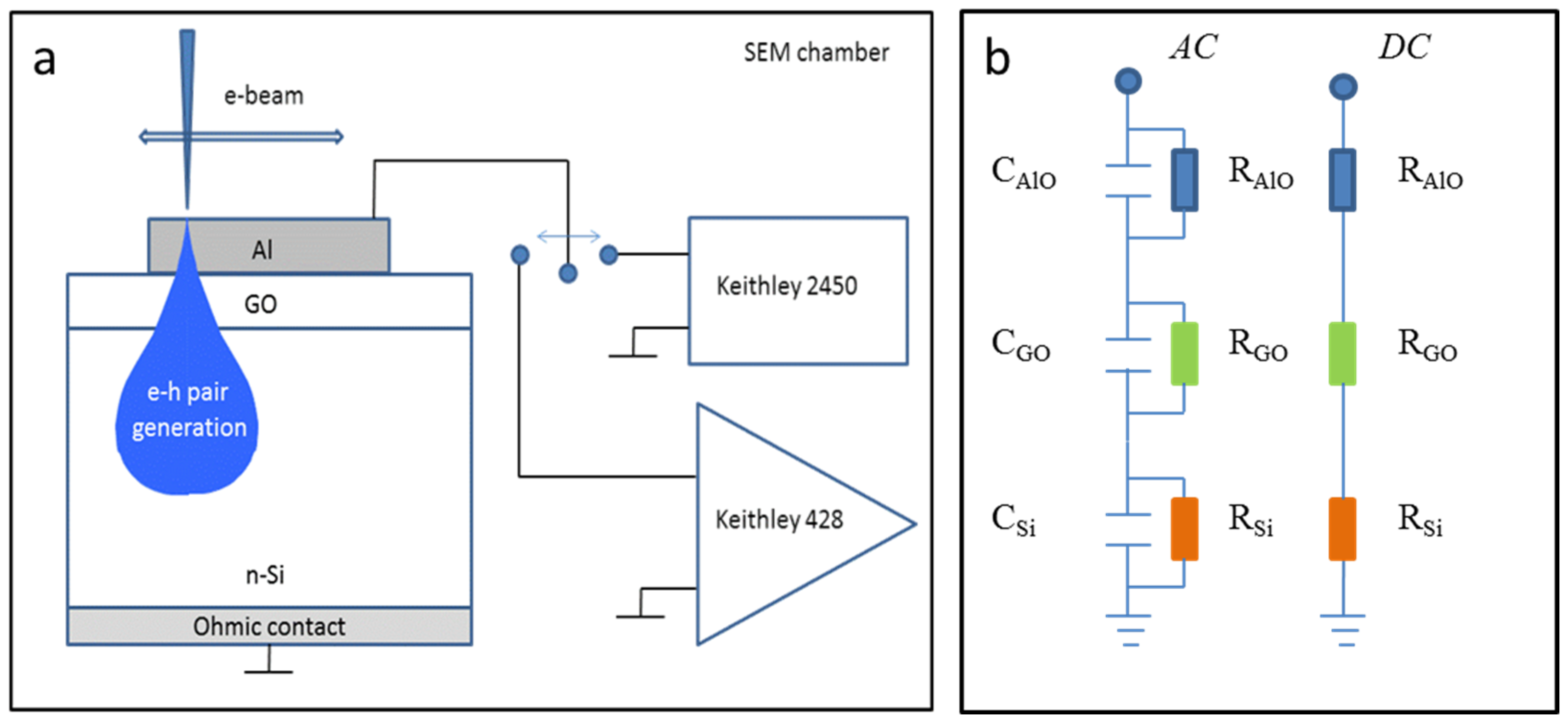
The investigations of the resistive switching characteristics and operative switching mechanisms in the GO films were carried out on the MIS structures that were made on phosphorous-doped Si wafer pieces with the GO film thickness of 40 nm. The top electrodes of circular shape and 1 mm in diameter were made by the sputtering of Al or Pt; the ohmic contact to the bottom Si electrode was formed by scratching the InGa paste. The use of the MIS structures with the bottom electrode of the n-type silicon allows us to determine the charges in the graphene oxide, evaluate its dielectric permittivity and provide the injection of holes under the negative bias that was applied to the top electrode. The use of aluminum as a top metal electrode allows the experimental verification of one of the switching mechanisms that is listed above, whereas Al fusibility can be employed to visualize the conductive channels under a high current flow. The use of the MIS structures also makes it possible to apply the method of electron beam-induced current to detect the conductive channels that are formed during the resistive switching processes. The GO film switching characteristics were studied by the DC current–voltage measurements using the Keithley 2450 Source Meter. To evaluate the presence of the charge traps in the GO film, the capacitance–voltage (C–V) characteristics were measured using the Keithley 4200A-SCS parametric analyzer at 100 kHz. The EBIC study was carried out using the scanning electron microscope (SEM) Jeol JSM-840 and using the Keithly 428 current amplifier at room temperature with a beam energy that was in the range from 8 keV to 30 keV and a beam current that was lower than 10
−11 A to minimize the irradiation dose. To monitor the e-beam irradiation effect during the EBIC mapping, the switching characteristics were measured on more than 20 MOS structures before and after their irradiation with an electron beam. After the experiments on resistive switching and the EBIC characterization, the aluminum electrodes were chemically removed, and the underlying GO film was characterized using the SENTERRA Bruker Raman microscope at the laser wavelength of 532 nm. A schematic presentation of the MIS structure and the experimental setup for the current–voltage and EBIC measurements is given in
Figure 1a. The device was placed into the SEM chamber, where an electron beam was turned off during the measurements of current–voltage characteristics. An electron beam generates electron–hole pairs at different depth depending on the beam energy. As it is discussed below, the electrons and holes are separated by an internal electric field; the generated holes are driven towards the Al electrode and contribute to the collected current, the value of which determines the brightness of an EBIC image.
Figure 1b presents the equivalent circuits of the Al/GO/n-Si MIS structure under the
AC and
DC measurements, respectively. Note that the capacitance playing a major role during the C–V measurements at a frequency of 100 kHz had an infinite value during the
DC voltage sweep. The presence and role of aluminum oxide are explained in
Section 3.4.
4. Discussion
The results of the current–voltage and EBIC measurements that are presented in
Figure 2 and
Figure 3, respectively, indicate that the HRS-to-LRS transition under the voltage sweep results in the formation of multiple conductive paths in the graphene oxide. Due to a complex structure of the graphene oxide film, both the number and locations of the point-like conductive channels across the film area are quite random and vary from device to device. Some of these conductive channels disappear under the voltage sweep of the opposite polarity, while several new channels are formed. This feature may indicate either a different origin of the formed conductive channels, or a different mechanism that governs the resistive switching. Some of the conductive channels can be associated with metallic-like conductive filaments, while the others—with the presence of sp2 graphene domains in an oxygen-enriched sp3 matrix of a pristine film or with a local thinning of the insulating GO layer, thereby resulting in a correspondent increase in an electric field.
Based on the analysis that is presented in
Section 3.2, it was shown that the detection of the conductive channels in the Al/GO/n-Si MIS structures by EBIC was possible due to the formation of local rectifying contacts at the conductive channel/Si interfaces. A rectifying contact that is formed during resistive switching must over-compensate the impact of a positive charge (
Figure 6a) in the bulk of the pristine GO film in order to separate the electrons and holes using a built-in internal electric field. This is a fundamentally important requirement for the drift of the holes towards the top electrode and for their contribution to the collected current that is responsible for detection of the conductive channels by EBIC. The evidence of the major contribution of the holes that are generated by an electron beam to the collected current was experimentally established (
Section 3.2). Although the origin of such a rectifying barrier is unknown, it is reasonable to suggest that an applied electric field results in either creation of negatively charged traps or an increase in GO work function near the interface of a conductive channel with silicon. The formation of the rectifying contacts implies that all of the conductive channels that are revealed by the EBIC must be located in close vicinity to or directly at the GO/Si interface.
The transitions from HRS to LRS are seen when a negative voltage was applied to the top electrode (
Figure 2). In this case, the multiple local conductive channels that were revealed by EBIC (
Figure 3) could be formed due to the upward drift of the positively charged oxygen vacancies in the GO or caused by the drift of cations in the opposite direction. Along with an observed decrease in the current (
Figure 2b), some of these conductive filaments were found to disappear under the applied voltage of an opposite polarity (
Figure 3f), thus demonstrating a typical bipolar resistive switching behavior. These findings strongly support the model of metallic-like filamentary conduction [
5,
6,
11]. Therefore, it is reasonable to assume that the physical mechanism that is responsible for the LRS-to-HRS transition is based on the destruction of the conductive filaments, consisting of either oxygen vacancies or cations that have accumulated near/at the GO/Si interface.
According to the data in [
8], the conductive filaments consisting of the sp2 fragments in the sp3 domain can be formed under an electric field and provide stable conductive paths. The EBIC data that were obtained using the devices after the resistive switching at a high compliance current of 100 mA indicate that some of the conductive channels occupy a large area that is comparable to the size of the GO flakes (
Figure 5a,d). Although a Raman investigation of these areas (
Figure 5b,c) did not reveal direct evidence of the sp3-to-sp2 transition in the GO bulk, the data clearly indicate that the large GO areas with an increased and uniform conductivity were not related to the GO thickness variations. The experimental verification of the sp3-to-sp2 transitions in the GO bulk under an electric field should be continued on the structures with semi-transparent metal electrodes to avoid the GO film oxidation during the procedure of the metal removal.
The role of aluminum oxide in the resistive switching of the Al/GO structures was discussed in [
7], where it was demonstrated that the surface of the GO film was reduced, while the aluminum at the interface with GO was oxidized. The presence of a thin aluminum oxide layer in the Al/GO/n-Si MIS structures that were used in the present work was demonstrated by results of the capacitance–voltage measurements (
Figure 6). In particular, the accumulation capacitance was found to notably increase after increasing the negative voltage that was applied to the top electrode to at least 4 V. (
Figure 6a). This can be explained by a series connection of graphene oxide with aluminum oxide (see
AC equivalent circuit in
Figure 1b). A negative bias that is applied to the Al electrode initiates the upward drift of the oxygen vacancies which create conductive paths in a thin aluminum oxide layer that, in turn, results in the electrical shortening of the aluminum oxide. As a consequence, the accumulation capacitance is determined by the thickness of the GO layer only, and hence, it increases. The values of both of the capacitances (the capacitance of graphene and aluminum oxides which are connected in series and the capacitance after the aluminum oxide shortening) are known from the C–V characteristics (
Figure 6b). Therefore, the capacitance of the aluminum oxide layer and hence its thickness can be determined. Assuming that the aluminum oxide dielectric constant is in a range that spans from seven to nine, then the aluminum oxide thickness is estimated to be between 2.5 nm and 3.2 nm. It should be noted that the conductive channels in the aluminum oxide cannot be directly detected by the EBIC due to the GO layer separating them from the GO/Si interface. However, due to their contribution to the series resistance, the conductive channels in the aluminum oxide can affect the brightness of the EBIC images that are shown in
Figure 3. Thus, the observed data strongly support the model of the contact resistance modification [
7]. In this model, the resistive switching is attributed to the formation and rupture of the local filaments in a thin insulating layer at the interface with a top Al electrode.
To illustrate the formation and disappearance of the conductive channels in the Al/GO/n-Si MIS structure,
Figure 7 presents the simple equivalent circuits of the device before and after the resistive switching. A symbol of a diode in
Figure 7a illustrates a potential barrier that is formed at the GO/Si interface due to a positive charge in the pristine GO film. After the HRS-to-LRS transition (green dash-lined rectangle in
Figure 7b), the initial resistance of the aluminum oxide layer R
AlO was strongly reduced to R*
AlO due to the formation of multiple metallic-like conductive filaments under relatively low voltages. Conductive filaments in the GO (R*
GO) are formed at higher voltages, and they can be directly detected by the EBIC due to the formation of local rectifying barriers at the GO/Si interface. These local barriers over-compensate a barrier in the pristine GO film, as shown by the change in the diode polarity in
Figure 7b. Some of the local conductive channels in the GO can be aligned with the conductive filaments in the aluminum oxide as denoted by a thicker line connecting the GO and the aluminum oxide layers. After the LRS-to-HRS transition (blue dash-lined rectangle in
Figure 7b), some of the conductive channels in the GO disappear (
Figure 3f) due to a full or partial elimination of the conductive filaments. The transition of some of the channels to HRS is accompanied by a polarity change in a rectifying barrier (denoted as 2*), while no barrier change occurs for the other channels (denoted as 1*). This difference illustrates the different mechanisms governing the change in the conductive channel resistance, i.e., reduction in the length of a conductive filament and/or sp2-to sp3-transition. The sub-circuit 3* illustrates the case when some channels remain unchanged during the LRS-to-HRS transition, while some of the new channels are formed as observed in the EBIC (
Figure 3f).
The presence of the GO bulk traps for the holes was established by measuring the GO-based MIS capacitors (
Figure 6). A notable shift of the C–V curve (
Figure 6a) indicates the accumulation of a positive charge in the GO bulk traps. Although the specific location of these traps within the GO bulk is not known, they can participate in the resistive switching processes.


 ,
, 