Abstract
The applications of thin-film transistors (TFTs) based on oxide semiconductors are limited due to instability under negative bias illumination stress (NBIS). Here, we report TFTs based on solution-processed In2O3 semiconductors doped with Pr4+ or Tb4+, which can effectively improve the NBIS stability. The differences between the Pr4+-doped In2O3 (Pr:In2O3) and Tb4+-doped In2O3 (Tb:In2O3) are investigated in detail. The undoped In2O3 TFTs with different annealing temperatures exhibit poor NBIS stability with serious turn-on voltage shift (ΔVon). After doping with Pr4+/Tb4+, the TFTs show greatly improved NBIS stability. As the annealing temperature increases, the Pr:In2O3 TFTs have poorer NBIS stability (ΔVon are −3.2, −4.8, and −4.8 V for annealing temperature of 300, 350, and 400 °C, respectively), while the Tb:In2O3 TFTs have better NBIS stability (ΔVon are −3.6, −3.6, and −1.2 V for annealing temperature of 300, 350, and 400 ℃, respectively). Further studies reveal that the improvement of the NBIS stability of the Pr4+/Tb4+:In2O3 TFTs is attributed to the absorption of the illuminated light by the Pr/Tb4f n—O2p6 to Pr/Tb 4f n+1—O2p5 charge transfer (CT) transition and downconversion of the light to nonradiative transition with a relatively short relaxation time compared to the ionization process of the oxygen vacancies. The higher NBIS stability of Tb:In2O3 TFTs compared to Pr:In2O3 TFTs is ascribed to the smaller ion radius of Tb4+ and the lower energy level of Tb 4f 7 with a isotropic half-full configuration compared to that of Pr 4f 1, which would make it easier for the Tb4+ to absorb the visible light than the Pr4+.
Keywords:
praseodymium; terbium; tetravalent; oxide semiconductors; thin-film transistors; stability 1. Introduction
Oxide semiconductors, such as InGaZnO4 (IGZO) [1,2,3,4,5], have drawn considerable attention for the advantages of relatively high mobility, large-area processability, good uniformity, high transparency to visible light, etc. [6] In particular, the extremely low off current (Ioff) makes it attractive in energy-saving devices that require long stand-by time [7]. However, a critical technical issue remains to be solved for better device applications of the thin-film transistors (TFTs) based on oxide semiconductors. Although oxide semiconductors are highly transparent in the visible range, they suffer from serious threshold voltage (Vth) change under negative bias illumination stress (NBIS) even when illuminated by visible light with smaller photon energies than their bandgaps [8,9,10,11,12]. Although the NBIS instability of the oxide TFTs have been studied intensively over the past decade, no consensuses have been reached on the mechanism of the NBIS instability [6].
Our previous work shows that the doping of tetravalent lanthanides (Ln)—praseodymium (Pr4+) and terbium (Tb4+)—can improve the NBIS stability of the oxide TFTs greatly [13]. However, the insightful effects of the tetravalent lanthanides on photostability of the oxide TFTs is still unclear. In this paper, the differences between Pr4+ and Tb4+ doped oxide semiconductors are compared in detail, and new experiments and analysis (such as low-temperature measurements) are carried out to give a more insightful understanding of the mechanism of the NBIS instability of oxide TFTs and the intrinsic effect of Pr4+/Tb4+ on the electrical and optical properties of oxide TFTs.
2. Experimental Section
2.1. Precursor Solutions
The oxide semiconductor films were deposited by spin-coating and thermal decomposition of precursor solutions. A 0.2 M In2O3 solution was prepared by dissolving indium nitrate hydrate ((In(NO)3·nH2O), Sigma-Aldrich, Tianhe District, Guangzhou, China) in deionized water. The Ln:In2O3 precursor solutions were synthesized by dissolving indium nitrate hydrate ((In(NO)3·nH2O), Sigma-Aldrich, Tianhe District, Guangzhou, China) and lanthanides nitrate hydrate (Pr/Tb(NO)3·nH2O, Aladdin, Industrial Co., Shanghai, China) in deionized water, which was optimized to the total concentration of metal ion of 0.2 M and In/Ln molar ratio of 19:1. All the precursor solutions were stirred vigorously for 12 h at room temperature and filtered through a 0.22 μm syringe filter before spin-coating.
2.2. Device Fabrication
A bottom-gate and top-contact structure was used to fabricate Ln:In2O3 TFT, as shown in Figure 1. First, a 300-nm-thick Al:Nd alloy film was deposited onto a glass substrate by sputtering and patterned by wet etch, followed by an anodization process to form a 200-nm-thickness Nd:AlOx gate dielectric layer on the surface of Al:Nd film [14]. Next, an ultraviolet light irradiating for a long time was used to treat a part (channel area) of the Nd:AlOx surface with a stencil shadow mask in order to form a hydrophilic surface in the channel area. The Ln:In2O3 precursor films were deposited onto the wettable area irradiated by UV by spin-coating the precursor solutions at 2000 rpm for 5 s and 6500 rpm for 40 s, followed by drying at 40 °C and thermal annealing at 300/350/400 °C for 1 h in an air condition. Then, the Al source and drain electrodes were deposited on the Ln: In2O3 layer by thermal evaporation and defined the channel area with 800 μm width (W) and 200 μm length (L) by using a stencil shadow mask. Finally, the devices were post-annealed at 300 °C for 1 h in an air condition.
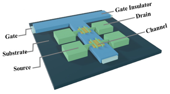
Figure 1.
Schematic structure of the TFTs with an anodized gate dielectric.
2.3. Characterization of Films and Devices
The electrical characteristics of the TFTs were measured using a semiconductor parameter analyzer system in conjunction with a probe station in a vacuum condition. The NBIS stability was tested by monitoring evolutions of the transfer curves of the TFTs as a function of the stress time under gate bias stresses of −20 V combined with white LED irradiation (250 Lux). The crystallization characteristics of the films were determined by X-ray diffraction (XRD) experiments. The chemical shift of different elements was characterized by the X-ray Photoelectron Spectroscopy (XPS).
3. Results and Discussion
3.1. TFT Characteristics
The transfer curves of the In2O3, Pr:In2O3, and Tb:In2O3 TFTs with different annealing temperature are shown in Figure 2a–c, respectively. All the TFTs showed increases on the current (Ion) and off current (Ioff) with increasing annealing temperatures, which reflects that the channels became more conductive as the annealing temperature increased. Compared to those of the Pr:In2O3 and Tb:In2O3 TFTs, the In2O3 TFTs displayed higher Ioff, more negative Vth, and more sensitivity to the annealing temperature, which reflects that both Pr and Tb can reduce the free carriers. The saturation mobility (μsat) of TFTs were calculated using Equation (1).
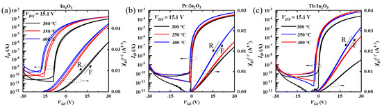
Figure 2.
Transfer curves of the (a) In2O3, (b) Pr:In2O3 TFTs, and (c) Tb:In2O3 TFTs; all of the curves recorded both forward (F) and reverse (R) gate sweeps.
The properties of the In2O3, Pr:In2O3, and Tb:In2O3 TFTs are summarized in Table 1. Although the In2O3 TFTs had higher mobility, they exhibited large hysteresis in the transfer curves between forward and reverse gate sweeps, which suggests that the In2O3 TFTs were in a rather unstable state even annealed at 400 °C. For Pr:In2O3 TFTs, the mobility increased slightly from 5.0 to 6.1 cm2·V−1·s−1 as the annealing temperature increased from 300 °C to 350 °C; when the annealing temperature further increased to 400 °C, the mobility increased largely to 10.1 cm2·V−1·s−1. For Tb:In2O3 TFTs, the mobility at 300 °C annealing temperature was only 4.7 cm2·V−1·s−1, which was a bit lower than that of the Pr:In2O3 TFTs. As the annealing temperature increased to 350 °C, the mobility increased significantly to 13.4 cm2·V−1·s−1, which was much higher than that of the Pr:In2O3 TFTs. When the annealing temperature further increased to 400 °C, the mobility further increased to as high as 18.2 cm2·V−1·s−1. It can be briefly summarized that, at a low annealing temperature (300 °C), the Pr:In2O3 TFT and Tb:In2O3 TFT showed little difference on mobility, but at high annealing temperature (350/400 °C), the Tb:In2O3 TFTs had much higher mobilities than the Pr:In2O3 TFTs.

Table 1.
Summary of the properties of the Pr/Tb:In2O3 TFTs with different annealing temperatures.
3.2. Film Structures
As known, in solution-processed oxide semiconductors, increasing annealing temperature is good for reducing the chemical residues and hence increasing the mobility, which is consistent with the results summarized in Table 1 [15]. For TFTs with the same annealing temperature (350 or 400 °C), the higher mobility of the Tb:In2O3 TFTs compared to that of the Pr:In2O3 TFTs may be attributed to the smaller ions radius of the Tb ions compared to the corresponding Pr ions. Unlike most of the other elements, lanthanides with larger atomic numbers have smaller ion radii due to the lanthanide contradiction, so Tb has a smaller ion radius (0.92 Å for Tb3+, and 0.76 Å for Tb4+) than Pr (0.99 Å for Pr3+, and 0.85 Å for Pr4+). Therefore, the ion radius of Tb is closer to that of In3+ (0.80 Å) compared to those of Pr, which may result in being easier to incorporate into the In2O3 lattice of Tb than Pr. The structures of the solution-processed Pr:In2O3 and Tb:In2O3 films annealed at different temperature were characterized by XRD experiments, as shown in Figure S1. All of the films showed a relatively strong diffraction peak around 30.6°, which is close to the (222) of the bixbyite In2O3, and a weak diffraction peak around 35.2°, which is close to the (400) of the bixbyite In2O3. Both Pr:In2O3 and Tb:In2O3 films exhibited better crystallinity as the annealing temperature increased. The 300 °C-annealing Tb:In2O3 film exhibited a much stronger (222) diffraction peak than the 300 °C-annealing Pr:In2O3 one. For the films annealed at higher temperatures (350 and 400 °C), there were no clear differences in the (222) diffraction peaks between Pr:In2O3 and Tb:In2O3, but the Tb:In2O3 showed a stronger (400) peak than the Pr:In2O3. Interestingly, the diffraction peak of the Pr:In2O3 film was almost in the same position as that of In2O3 film, while the diffraction peak of the Tb:In2O3 film exhibited an apparent left shit (~0.2°) compared to the standard (222) diffraction peak of the pure In2O3. The result implied that the Tb ions (at least some of them) may incorporate into the In2O3 lattice (causing lattice expansion) while most of the Pr ions may not incorporate into the In2O3 lattice (still In2O3 phase after Pr doping). Compared to the Pr:In2O3 with separated phases of PrOx and In2O3, the Tb:In2O3 with Tb incorporated into the In2O3 lattice is better for carrier transport, which may result in higher mobility.
3.3. NBIS Instabilities
To further investigate the effect of Pr/Tb on the TFT properties, the stability of the TFTs were characterized under NBIS with a negative VG stress of −20 V combined with an illumination stress of 250-Lux white LED light. Figure 3 shows the transfer curve evolutions of different TFTs as a function of the stress time during NBIS. The Von shift (ΔVon, defined by the gate voltage shift at ID = 10−8 A) under 3600 s NBIS are summarized in Table 1. The In2O3 TFTs with different annealing temperatures exhibited poor NBIS stability with large ΔVon (the actual ΔVon of the In2O3 TFTs was much larger than the measured ΔVon, as discussed below). After doping with Pr/Tb, the TFTs showed greatly improved NBIS stability. Surprisingly, the Pr:In2O3 and the Tb:In2O3 TFTs exhibited different temperature-dependent trends. As the annealing temperature increased, the Pr:In2O3 TFTs had poorer NBIS stability (ΔVon were −3.2, −4.8, and −4.8 V for annealing temperature of 300, 350, and 400 °C, respectively), while the Tb:In2O3 TFTs had better NBIS stability (ΔVon were −3.6, −3.6, and −1.2 V for annealing temperatures of 300, 350, and 400 ℃, respectively).
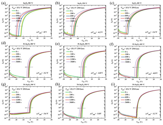
Figure 3.
Variations of time-dependent transfer curves under NBIS (a negative gate bias stress of −20 V combined with white LED light illumination of 250 Lux) for the TFTs with channels of In2O3 (annealed at (a) 300 °C, (b) 350 °C, (c) 400 °C), Pr:In2O3 (annealed at (d) 300 °C, (e) 350 °C, (f) 400 °C), and Tb:In2O3 (annealed at (g) 300 °C, (h) 350 °C, (i) 400 °C).
It should be noted that the Von of all the undoped-In2O3 TFTs with different annealing temperatures reached the negative limit of −20 V (the voltage of the stressing gate bias) after 3600 s NBIS, which means that the actual ΔVon of the undoped-In2O3 TFTs was much larger than the measured ΔVon. To confirm the dependence of the Von shift limit on the stressing gate bias, the TFTs were characterized under NBIS with a more negative stressing gate bias of −30 V combined with an illumination stress of 250-Lux white LED light. Figure S2 shows the evolutions of the transfer curves of different TFTs under −30 V NBIS as a function of the stress time. The ΔVon of the In2O3 TFTs under −30 V NBIS were much larger than those under −20 V NBIS, and the negative limit of the Von of the In2O3 TFTs after NBIS is close to −30 V. Thus, the NBIS instability of the In2O3 TFTs were much more serious than measured. In contrast to the undoped In2O3 TFTs, the Pr/Tb:In2O3 TFTs did not show much difference for ΔVon under −30 V NBIS, as shown in Figure S3.
3.4. Oxygen Vacancies
It has been reported that the decrease in VO concentration of the IGZO can improve the NBIS stability effectively [16]. Compared to the IGZO, the In2O3 has much higher VO concentration. Although the lanthanide doping can reduce the VO concentration and suppress the free carrier generation of the In2O3, the VO concentration is still much higher than that of the IGZO. Here, the large improvement of NBIS stability after Pr/Tb doping is not mainly due to the reduction of the VO concentration, because there are no direct relationships between the NBIS stability and the VO concentration [13,17,18]. For example, the Pr:In2O3 had much higher VO concentration than Tb:In2O3 (see Figure 4) for annealing temperature of 300 ℃, but it did not exhibit much difference in NBIS stability compared with Tb:In2O3. The In2O3 doped with another lanthanide element gadolinium (Gd, which has low electronegativity and large metal–oxide bonding energy that is comparable to those of Pr and Tb) had a low VO concentration, but the Gd:In2O3 TFT had poor NBIS stability with ΔVon of as large as −13.9 V [13] for Pr:In2O3 annealed at 400 °C, the VO concentration reduced greatly compared to the one annealed at 300 °C, but its NBIS stability was not as good as the one annealed at 300 °C. Thus, the reduction of VO concentration is not the main reason for the large improvement of NBIS stability after Pr/Tb doping.
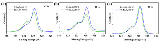
Figure 4.
O 1s XPS spectra of Pr/Tb:In2O3 annealed at (a) 300, (b) 350, and (c) 400 °C.
3.5. Temperature-Dependent Performances
To further investigate the intrinsic mechanism of the NBIS stability, the NBIS stability measurements were performed at different temperatures (from 78 K to 295 K). Figure 5 shows the ΔVon evolution of the different TFTs under NBIS, and Figure S4 shows the corresponding evolutions of the transfer curves of different TFTs under NBIS. All of the TFTs showed decreasing Ion with decreasing measuring temperature, which implies that trap-limited conduction (TLC) becomes dominant at a low temperature. In oxide semiconductors, both TLC and percolation conduction (PC) exist (see Figure 6) [19,20]. In TLC, the electrons are subjected to multiple trapping events in the localized tail states below the conduction band edge (Em), and the transport between tail states is via the variable range hopping (VRH) [20]. At this low temperature, the electrons are more likely to be trapped in the localized tail states due to the lack of sufficient thermal energy, thus the mobility decreases as the measuring temperature decreases. As a result, the conductivity of the oxide semiconductors reduces greatly at a low temperature, which is consistent with the reduction of the Ion of the TFTs at low temperatures (see Figure S4).
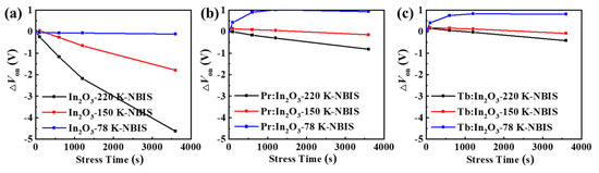
Figure 5.
ΔVon evolutions of the TFTs with (a) pure In2O3, (b) Pr:In2O3, and (c) Tb:In2O3 under NBIS with different temperatures of 78 K, 150 K, and 220 K.
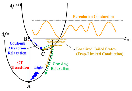
Figure 6.
Illustration of the CT transition process in Pr4+/Tb4+ doped In2O3.
It could also be seen from Figure 5 and Figure S4 that all devices displayed decreasing ΔVon with decreasing temperature. Surprisingly, when the measuring temperature decreased to 78 K, the pure In2O3 TFT showed little ΔVon after 3600 s NBIS, while the Pr:In2O3 and Tb:In2O3 TFTs exhibited positive ΔVon of +1.0 V and +0.8 V, respectively. For comparison, the stability under negative bias stress (NBS) without light illumination were tested at room temperature, as shown in Figure S5. Only the pure In2O3 TFTs showed obvious ΔVon of −3.2 V after 3600 s NBS at room temperature (while the Pr/Tb:In2O3 TFTs exhibited neglectable ΔVon). The results reflect that the NBIS instability is a combined effect of light illumination and temperature (thermal activation), as well as gate bias. The energy of the white LED light (or blue light) is not enough to activate the deep donates (such as VO) near valance band maximum (VBM) at low temperature (78 K), which is contrary to the concept that the activation energy of the subgap state formed by VO is lower than the energy of the blue LED light.
3.6. Mechanisms of NBIS Instability
Over the past decades, considerable research efforts have been made to understand the native defects/impurities present in oxide semiconductors, but the origin of the unintentional n-type conductivity and/or the NBIS instability of the oxide TFTs is still a subject of debate [21,22,23,24,25,26,27,28,29,30]. Specifically, defect formation and carrier generation, electron localization/transient behavior, as well as carrier scattering in an amorphous state are all far from being fully understood. However, there seems to be an undeclared consensus that the VO is the major defect in n-type oxide semiconductors. Very recent studies show that VO likely acts as both shallow and deep donors in In2O3 [21,22]. The localized valence tail states or the subgap states near VBM, which are determined not only by their density but also by the degree of localization (structural defects in the amorphous state), contribute to the optical absorption within the visible range, i.e., from 1.5 eV to 3 eV [17]. Under combined stress of light illumination, temperature, and negative gate bias, some of the VOs will be excited, delocalized free electrons to the conduction band [23,24,25,26,27]. The transition of the VO ground state to singly charged oxygen vacancy (Vo1+) or doubly charged oxygen vacancy (Vo2+) excited states causes spontaneous outward relaxation. The relaxation for VO to Vo2+ is strong because of the electrostatic repulsion of the two positive charges in Vo2+ (e.g., the four nearest In neighbors of the Vo2+ in In2O3 significantly relax outward by 9.3%, 9.6%, 7.7%, and 13%) [21]. The strong relaxation causes a very slow VO ionization/recombination process, which leads to a very long decade time of the photocurrent [28,29]. However, since the highest energy of the white LED light (the blue light, ~2.7 eV) is high enough for exciting some of the less-deep VO states directly at low temperatures, the VO ionization model cannot fully explain why the In2O3 TFTs exhibited little ΔVon at a low temperature (78 K).
Flewitt and Powell proposed a defect transition model to interpretate why the ΔVon is the combined effect of light illumination, temperature, and negative gate bias. According to the model, the electron donor defect (De) can transfer to the neighboring n-coordinated oxygen atom [O(―M)n] via oxygen interstitials (Oi) with the help of holes, forming a positively charged defect (Dh2+) at the site of the original O(―M)n: [30].
The energy barrier for oxygen vacancy migration via Oi for pure In2O3 is about 0.71 eV, which accounts for the requirement for the thermalization energy (certain temperature) to activate the VOs. Under negative gate bias, the conduction band tails are depleted of electrons, which suppresses Equation (3). However, as the bias is insufficient to pull the Fermi level down through the large number of De states, the localized valence band tail states can never be accumulated with holes, so Equation (2) is also suppressed. Only under light illumination combining with negative gate bias are holes in the valence band tail created, allowing the hole quasi-Fermi level to be pulled towards the valence band [30]. This permits Equation (2), and Dh states may be created at the expense of De states. Therefore, it is only the combination of photon illumination with energies sufficient to lead to hole generation in valence band tail states and certain temperature with thermalization energy higher than the energy barrier for oxygen vacancy migration as well as negative gate bias that will lead to the negative ΔVon, as observed experimentally.
3.7. Effect of the CT Transition of Pr4+/Tb4+ on the Photo Stability
The great improvement in NBIS stability of the Pr/Tb:In2O3 TFTs is ascribed to the charge transfer (CT) transition of the Pr4+ and Tb4+. It is known that tetravalent lanthanide ions (Ce4+, Pr4+ and Tb4+) have low CT transition energies that have broad-band absorption [31,32,33]. Compared to Ce4+, whose CT transition absorption is in the UV range, the CT transistor of Pr4+ and Tb4+ have broad absorption in the visible range [13,31]. To identify the existence of Pr4+/Tb4+ in the Pr/Tb:In2O3 films, X-ray photoelectron spectroscopy (XPS) experiments were performed. Figure 7 shows the Pr3d and Tb3d spectra of the Pr/Tb:In2O3 films. The peaks were fitted according to the analysis reported elsewhere [34,35]. The parameters of the fitting peaks for Pr3d and Tb3d are summarized in Tables S1 and S2, respectively. The ratio of Pr4+/Pr3+ or Tb4+/Tb3+ were calculated by the peak areas. There is a clear trend of Pr4+/Pr3+ < Tb4+/Tb3+ at the same annealing temperature. The higher content of Tb4+ in Tb:In2O3 compared to that of Pr4+ in Pr:In2O3 may be one of the reason for the higher mobility and stability of Tb:In2O3 TFTs compared to those of Pr:In2O3 TFTs because Tb4+ has a smaller radius with an isotropic half-full 4f 7 configuration and a quenched orbital moment. It should be noted that the 4f 7 configuration has a large magnetic moment that may scatter the carriers and decrease the mobility. It should be noted that the properties of the solution-processed Pr/Tb:In2O3 differed from those of the vacuum-processed ones greatly. We will not compare the difference between vacuum-processed Pr and Tb doped In2O3 TFTs this time. The more insightful mechanisms of the difference between Pr and Tb doped In2O3 is still under investigated and will be reported in the future.
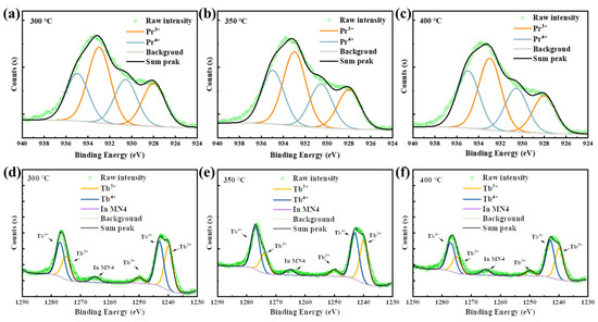
Figure 7.
Pr 3d XPS spectra of the Pr:In2O3 films annealed at (a) 300, (b) 350, and (c) 400 °C; Tb 3d XPS spectra of the Tb:In2O3 films annealed at (d) 300, (e) 350, and (f) 400 °C.
Figure 6 illustrates the CT transition process in Pr4+/Tb4+ doped In2O3. Initially, the system is at Point A on Parabola (4f n) corresponding with an electron at the top of the valence band and a Ln4+ ion (Ln4f n—O2p6). Under light illumination, the initial state transfers to Point B of the Ln3+ state (Ln4f n+1—O2p5). Due to Ln3+ having a larger ionic radius than Ln4+, it relaxes outward and moves to Point C. Then, it transfers back to Parabola (4f n) via crossing relaxation (by thermal activation) where all luminescence is quenched [36,37,38]. It should be noted that the Ln4f n—O2p6 to Ln4f n+1—O2p5 CT transition has smaller overall lattice expansion/contraction and shorter relaxation time compared to VO ionization because of the Coulomb attraction between the hole (O2p5) and the transferred electron [17,36]. As a result, the Ln4+ can more easily absorb light than VO. The results reveal that the improvement of the NBIS stability of the Pr/Tb:In2O3 TFTs is attributed to the absorption of the illuminated light by the Ln4f n—O2p6 to Ln4f n+1—O2p5 CT transition and downconversion of the light to nonradiative transition with a relatively short relaxation time compared to VO ionization. Minasian et al. reported that the partially occupied 4f states are lower in energy than the unoccupied 5d states and provide band gaps of 2.3 and 1.7 eV for PrO2 and TbO2, respectively [39]. The lower energy level of Tb 4f 7 compared to Pr 4f 1 would make it easier for the Tb4+ to absorb the visible light than the Pr4+, which may be the main reason for the higher NBIS stability of Tb:In2O3 TFTs compared to Pr:In2O3 TFTs.
The positive ΔVon under NBIS at a low temperature (78 K, see Figure 5 and Figure S4) of the Pr/Tb:In2O3 TFTs was ascribed to the further trapping of electrons by the Ln4f n+1 exciting states. At a low temperature, most of the electrons are localized in the tail states that intersect the Parabola (4f n+1), as shown in Figure 6. Under negative gate bias, these localized electrons are depleted and a part of them can further transit to Point C via the Parabola (4f n+1). As a result, the density of the localized electrons decreases, which is the reason why Pr/Tb:In2O3 TFTs exhibited positive ΔVon under NBIS at a low temperature.
3.8. Formatting of Mathematical Components
De + [O(—M)n2+2h] → De+Oi+Dh2+ → O(—M)n1 + Dh2+
Dh2+ + [O(—M)n1+2e] → Dh2++ Oi2-+ De → O(—M)n2 + De
4. Conclusions
In conclusion, TFTs based on solution-processed In2O3 semiconductors doped with Pr4+ or Tb4+ were investigated. It was found that both Pr4+ and Tb4+ can improve the NBIS stability greatly, but Tb4+ is better than Pr4+. The undoped In2O3 TFTs with different annealing temperatures exhibited poor NBIS stability with serious turn-on voltage shift. As the annealing temperature increased, the Pr:In2O3 TFTs had poorer NBIS stability (ΔVon are −3.2, −4.8, and −4.8 V for annealing temperatures of 300, 350, and 400 °C, respectively), while the Tb:In2O3 TFTs had better NBIS stability (ΔVon are −3.6, −3.6, and −1.2 V for annealing temperatures of 300, 350, and 400 °C, respectively). When the measuring temperature decreased to 78 K, the pure In2O3 TFT showed little ΔVon after 3600 s NBIS, while the Pr:In2O3 and Tb:In2O3 TFTs exhibited positive ΔVon of +1.0 V and +0.8 V, respectively. Further studies reveal that the negative ΔVon under NBIS is the combining effect of photon illumination with energies sufficient to lead to hole generation in valence band tail states, a certain temperature with thermalization energy higher than energy barrier for oxygen vacancy migration, and negative gate bias that will lead to bending of the energy band. The improvement of the NBIS stability of the Pr4+/Tb4+:In2O3 TFTs is attributed to the absorption of the illuminated light by the Pr/Tb4f n—O2p6 to Pr/Tb 4f n+1—O2p5 charge transfer (CT) transition and downconversion of the light to nonradiative transition with a relatively short relaxation time compared to ionization of oxygen vacancies. The positive ΔVon of the Pr/Tb:In2O3 TFTs under low temperature (78 K) is attributed to the further trapping of electrons by the 4f n+1 exciting states under negative bias. The higher NBIS stability of Tb:In2O3 TFTs compared to Pr:In2O3 TFTs is ascribed to the smaller ion radius of Tb4+ and the lower energy level of Tb 4f 7 compared to Pr 4f 1, which would make it easier for the Tb4+ to absorb the visible light than the Pr4+. It is worth noting that two sets of devices were tested, and the results can be considered typical.
Supplementary Materials
The following supporting information can be downloaded at: https://www.mdpi.com/article/10.3390/nano12213902/s1, Figure S1: XRD patterns of the Pr/Tb:In2O3 films annealed at different temperatures, and the bottom pattern is the standard refraction pattern of the single-crystal bixbyite In2O3; Figure S2: The variations of time-dependent transfer curves under NBIS (a negative gate bias stress of −30 V combining with white LED light illumination of 250 Lux) for the TFTs with channels of In2O3 annealed at (a) 300, (b) 350, and (c) 400 °C; Figure S3: The variations of time-dependent transfer curves under NBIS (a negative gate bias stress of −30 V combining with white LED light illumination of 250 Lux) for TFTs with channels of (a) Pr:In2O3 and (b) Tb:In2O3 annealed at 400 °C; Figure S4: Variations of time-dependent transfer curves under NBIS with different temperatures of 78 K, 150 K, and 220 K (a negative gate bias stress of −20 V combining with white LED light illumination of 250 Lux) for TFTs with channels of In2O3 (measured under (a) 78 K, (b)150 K, (c) 220 K), Pr:In2O3 (measured under (d) 78 K, (e)150 K, (f) 220 K), and Tb:In2O3 (measured under (g) 78 K, (h)150 K, (i) 220 K); Figure S5: Variations of time-dependent transfer curves under NBS without light illumination at room temperature for the TFTs with channels of (a) In2O3, (b) Pr:In2O3, and (c) Tb:In2O3; Table S1: Summary of the parameters of the fitting peaks of the XPS Pr 3d spectra in Figure 7; Table S2: Summary of the parameters of the fitting peaks of the XPS Tb 3d spectra in Figure 7.
Author Contributions
Conceptualization, L.L. and C.D.; methodology, C.D. and P.H.; formal analysis, L.L., J.P., H.S., B.H. and J.X.; investigation, C.D. and P.H.; writing—original draft preparation, L.L. and C.D.; writing—review and editing, L.L., J.P. and S.Z.; funding acquisition, L.L., J.P. and S.Z. All authors have read and agreed to the published version of the manuscript.
Funding
This work was supported in part by the National Natural Science Foundation of China under Grant 51673068, 61204087, and 51173049; in part by the Guangdong Project of Research and Development Plan in Key Areas under Grant 2020B010180001 and 2019B010934001; in part by the Guangdong Major Project of Basic and Applied Basic Research under Grant 2019B030302007; and in part by Science and Technology Program Project of Guangzhou under Grant 201904010282).
Data Availability Statement
The data is available on reasonable request from the corresponding author.
Conflicts of Interest
The authors declare no conflict of interest.
References
- Nomura, K.; Ohta, H.; Takagi, A.; Kamiya, T.; Hirano, M.; Hosono, H. Room-Temperature Fabrication of Transparent Flexible Thin-Film Transistors Using Amorphous Oxide Semiconductors. Nature 2004, 432, 488–492. [Google Scholar] [CrossRef] [PubMed]
- Asal, K.; Henrique, L.G.; Pedro, B.; Jorge, M.; Ana, R.; Joana, V.P.; Rodrigo, M.; Elvira, F. Improving positive and negative bias illumination stress stability in parylene passivated IGZO transistors. Appl. Phys. Lett. 2016, 109, 051606. [Google Scholar]
- Yao, J.K.; Ye, F.; Fan, P. Ultraviolet laser damage mechanism of amorphous InGaZnO4 thin films. Opt. Mater. Express 2019, 9, 2545–2552. [Google Scholar] [CrossRef]
- Dekkers, H.F.W.; Van Setten, M.J.; Belmonte, A.; Chasin, A.V.; Subhechha, S.; Rassoul, N.; Glushkova, A.V.; Delhougne, R.; Kar, G.S. Deposition, Characterization, and Performance of Spinel InGaZnO4. ACS Appl. Electron. Mater. 2022, 4, 1238–1249. [Google Scholar] [CrossRef]
- Cha, S.K.; Im, S.; Kim, Y.S.; Baeck, J.; Noh, J.; Park, K.S.; Kim, J.J.; Yoon, S.Y. Density-Dependent Microstructures and Electromechanical Properties of Amorphous InGaZnO4 Semiconductors: An Ab Initio Study. ACS Appl. Electron. Mater. 2022, 4, 2545–2551. [Google Scholar] [CrossRef]
- Shi, J.; Zhang, J.; Yang, L.; Qu, M.; Qi, D.; Zhang, K.H.L. Wide Bandgap Oxide Semiconductors: From Materials Physics to Optoelectronic Devices. Adv. Mater. 2021, 33, 30. [Google Scholar] [CrossRef]
- Ting-Kuo, C.; Chin-Wei, L.; Shihchang, C. LTPO TFT Technology for AMOLEDs. SID Symp. Dig. Tech. Pap. 2019, 50, 545–548. [Google Scholar]
- Jung, H.Y.; Kang, Y.; Hwang, A.Y.; Lee, C.K.; Han, S.; Kim, D.H.; Bae, J.U.; Shin, W.S.; Jeong, J.K. Origin of the Improved Mobility and Photo-Bias Stability in a Double-Channel Metal Oxide Transistor. Sci. Rep. 2014, 4, 8. [Google Scholar] [CrossRef]
- Xu, H.; Xu, M.; Li, M.; Chen, Z.; Zou, J.; Wu, W.; Qiao, X.; Tao, H.; Wang, L.; Ning, H.; et al. Trap-Assisted Enhanced Bias Illumination Stability of Oxide Thin Film Transistor by Praseodymium Doping. ACS Appl. Mater. Interfaces 2019, 11, 5232–5239. [Google Scholar] [CrossRef]
- Li, J.; Fu, Y.Z.; Huang, C.X.; Zhang, J.H.; Jiang, X.Y.; Zhang, Z.L. Nitrogen Anion Doping as a Strategy to Suppress Negative Gate-Bias Illumination Instability of ZnSnO Thin Film Transistor. Appl. Phys. Lett. 2016, 108, 5. [Google Scholar] [CrossRef]
- Kim, J.; Bang, J.; Nakamura, N.; Hosono, H. Ultra-Wide Bandgap Amorphous Oxide Semiconductors for NBIS-Free Thin-Film Transistors. APL Mater. 2019, 7, 4. [Google Scholar] [CrossRef]
- Shiah, Y.S.; Sim, K.; Shi, Y.H.; Abet, K.; Ueda, S.; Sasase, M.; Kim, J.; Hosono, H. Mobility-Stability Trade-off in Oxide Thin-Film Transistors. Nat. Electron. 2021, 4, 800–807. [Google Scholar] [CrossRef]
- He, P.; Lan, L.; Deng, C.; Wu, Y.; Lin, Y.; Chen, S.; Ding, C.; Xu, M.; Peng, J. The Effect of Charge Transfer Transition on the Photostability of Lanthanide-Doped Indium Oxide Thin-Film Transistors. Commun. Mater. 2021, 2, 1–10. [Google Scholar] [CrossRef]
- Lan, L.; Zhao, M.; Xiong, N.; Xiao, P.; Shi, W.; Xu, M.; Peng, J. Low-Voltage High-Stability Indium-Zinc Oxide Thin-Film Transistor Gated by Anodized Neodymium-Doped Aluminum. IEEE Electron Device Lett. 2012, 33, 827–829. [Google Scholar] [CrossRef]
- Li, Y.; Lan, L.; Sun, S.; Lin, Z.; Gao, P.; Song, W.; Song, E.; Zhang, P.; Peng, J. All Inkjet-Printed Metal-Oxide Thin-Film Transistor Array with Good Stability and Uniformity Using Surface Energy Patterns. ACS Appl. Mater. Interfaces 2017, 9, 8194–8200. [Google Scholar] [CrossRef]
- Ryu, B.; Noh, H.K.; Choi, E.A.; Chang, K.J. O-vacancy as the origin of negative bias illumination stress instability in amorphous In-Ga-Zn-O thin film transistors. Appl. Phys. Lett. 2010, 97, 022108. [Google Scholar] [CrossRef]
- Lan, L.; Li, X.; Ding, C.; Chen, S.; Su, H.; Huang, B.; Chen, B.; Zhou, H.; Peng, J. The Effect of the Charge Transfer Transition of the Tetravalent Terbium on the Photostability of Oxide Thin-film Transistors. Adv. Electron. Mater. 2022, 8, 2200187. [Google Scholar] [CrossRef]
- Zhang, H.; Liang, L.; Wang, X.; Wu, Z.; Cao, H. Praseodymium-Doped In-Sn-Zn-O TFTs With Effective Improvement of Negative-Bias Illumination Stress Stability. IEEE Trans. Electron Devices 2022, 69, 152–155. [Google Scholar] [CrossRef]
- Nomura, K.; Kamiya, T.; Ohta, H.; Ueda, K.; Hirano, M.; Hosono, H. Carrier Transport in Transparent Oxide Semiconductor with Intrinsic Structural Randomness Probed Using Single-Crystalline InGaO3(ZnO)(5) Films. Appl. Phys. Lett. 2004, 85, 1993–1995. [Google Scholar] [CrossRef]
- Lee, S.; Ghaffarzadeh, K.; Nathan, A.; Robertson, J.; Jeon, S.; Kim, C.; Song, I.H.; Chung, U.I. Trap-Limited and Percolation Conduction Mechanisms in Amorphous Oxide Semiconductor Thin Film Transistors. Appl. Phys. Lett. 2011, 98, 3. [Google Scholar] [CrossRef]
- Chatratin, I.; Sabino, F.P.; Reunchan, P.; Limpijumnong, S.; Varley, J.B.; Van de Walle, C.G.; Janotti, A. Role of Point Defects in the Electrical and Optical Properties of In2O3. Phys. Rev. Mater. 2019, 3, 9. [Google Scholar] [CrossRef]
- Medvedeva, J.E.; Zhuravlev, I.A.; Burris, C.; Buchholz, D.B.; Grayson, M.; Chang, R.P.H. Origin of High Carrier Concentration in Amorphous Wide-bandgap Oxides: Role of Disorder in Defect Formation and Electron Localization in In2O3-x. J. Appl. Phys. 2020, 127, 24. [Google Scholar] [CrossRef]
- Janotti, A.; Walle, C.G.V.D. Oxygen Vacancies in ZnO. Appl. Phys. Lett. 2005, 87, 125210. [Google Scholar] [CrossRef]
- Lany, S.; Zunger, A. Anion Vcancies as a Source of Persistent Photoconductivity in II-VI and Chalcopyrite Semiconductors. Phys. Rev. B 2005, 72, 13. [Google Scholar] [CrossRef]
- Janotti, A.; Walle, C. Native Point Defects in ZnO. Phys. Rev. B 2007, 76, 165202. [Google Scholar] [CrossRef]
- Jeong, J.K. Photo-Bias Instability of Metal Oxide Thin Film Transistors for Advanced Active Matrix Displays. J. Mater. Res. 2013, 28, 2071–2084. [Google Scholar] [CrossRef]
- Long, T.; Dai, X.; Lan, L.; Deng, C.; Chen, Z.; He, C.; Liu, L.; Yang, X.; Peng, J. High-Performance CdScInO Thin-Film Transistors and Their Stability Improvement under Negative Bias (Illumination) Temperature Stress. J. Mater. Chem. C 2019, 7, 13960–13965. [Google Scholar] [CrossRef]
- Lee, D.H.; Kawamura, K.; Nomura, K.; Kamiya, T.; Hosono, H. Large Photoresponse in Amorphous In-Ga-Zn-O and Origin of Reversible and Slow Decay. Electrochem. Solid State Lett. 2010, 13, II324–II327. [Google Scholar] [CrossRef]
- Mondal, S.; Raychaudhuri, A.K. Observation of a Large Gate-controlled Persistent Photoconduction in Single Crystal ZnO at Room Temperature. Appl. Phys. Lett. 2011, 98, 3. [Google Scholar] [CrossRef]
- Flewitt, A.J.; Powell, M.J. A Thermalization Energy Analysis of the Threshold Voltage Shift in Amorphous Indium Gallium Zinc Oxide Thin Film Transistors under Simultaneous Negative Gate Bias and Illumination. J. Appl. Phys. 2014, 115, 7. [Google Scholar] [CrossRef]
- Hobart, D.E.; Samhoun, K.; Young, J.P.; Norvell, V.E.; Peterson, J.R. Stabilization of Praseodymium(IV) and Terbium(IV) in Aqueous Carbonate Solution. Chem. Inf. 1980, 11, 321–328. [Google Scholar] [CrossRef]
- Blasse, G. Luminescence of Inorganic Solids: From Isolated Centres to Concentrated Systems. Prog. Solid State Chem. (UK) 1988, 18, 79–191. [Google Scholar] [CrossRef]
- Gorai, T.; Schmitt, W.; Gunnlaugsson, T. Highlights of the Development and Application of Luminescent Lanthanide Based Coordination Polymers, MOFs and Functional Nanomaterials. Dalton Trans. 2021, 50, 770–784. [Google Scholar] [CrossRef] [PubMed]
- Kim, J.S.; Na, C.W.; Kwak, C.H.; Li, H.Y.; Yoon, J.W.; Kim, J.H.; Jeong, S.Y.; Lee, J.H. Humidity-Independent Gas Sensors Using Pr-Doped In2O3 Macroporous Spheres: Role of Cyclic Pr3+/Pr4+ Redox Reactions in Suppression of Water-Poisoning Effect. ACS Appl. Mater. Interfaces 2019, 11, 25322–25329. [Google Scholar] [CrossRef]
- Gu, S.; Li, W.; Bian, Y.; Wang, F.; Li, H.; Liu, X. Highly-Visible-Light Photocatalytic Performance Derived from a Lanthanide Self-Redox Cycle in Ln2O3/BiVO4 (Ln: Sm, Eu, Tb) Redox Heterojunction. J. Phys. Chem. C 2016, 120, 19242–19251. [Google Scholar] [CrossRef]
- Dorenbos, P. Systematic Behaviour in Trivalent Lanthanide Charge Transfer Energies. J. Phys.-Condes. Matter 2003, 15, 8417–8434. [Google Scholar] [CrossRef]
- Holsa, J.; Aitasalo, T.; Jungner, H.; Lastusaari, M.; Niittykoski, J.; Spano, G. Role of Defect States in Persistent Luminescence Materials. J. Alloy. Compd. 2004, 374, 56–59. [Google Scholar] [CrossRef]
- Zych, E.; Deren, P.J.; Strek, W.; Meijerink, A.; Mielcarek, W.; Domagala, K. Preparation, X-ray Analysis and Spectroscopic Investigation of Nanostructured Lu2O3: Tb. J. Alloy. Compd. 2001, 323, 8–12. [Google Scholar] [CrossRef]
- Minasian, S.G.; Batista, E.R.; Booth, C.H.; Clark, D.L.; Keith, J.M.; Kozimor, S.A.; Lukens, W.W.; Martin, R.L.; Shuh, D.K.; Stieber, S.C.E.; et al. Quantitative Evidence for Lanthanide-Oxygen Orbital Mixing in CeO2, PrO2, and TbO2. J. Am. Chem. Soc. 2017, 139, 18052–18064. [Google Scholar] [CrossRef]


Publisher’s Note: MDPI stays neutral with regard to jurisdictional claims in published maps and institutional affiliations. |
© 2022 by the authors. Licensee MDPI, Basel, Switzerland. This article is an open access article distributed under the terms and conditions of the Creative Commons Attribution (CC BY) license (https://creativecommons.org/licenses/by/4.0/).