
Strengthening Analysis of Ni-Sn Alloy Layer by Double Alloying Method Combined with First-Principles Calculation

Abstract
:1. Introduction
2. Materials and Methods
2.1. Experimental Procedures
2.2. Theoretical Calculation Method
3. Results
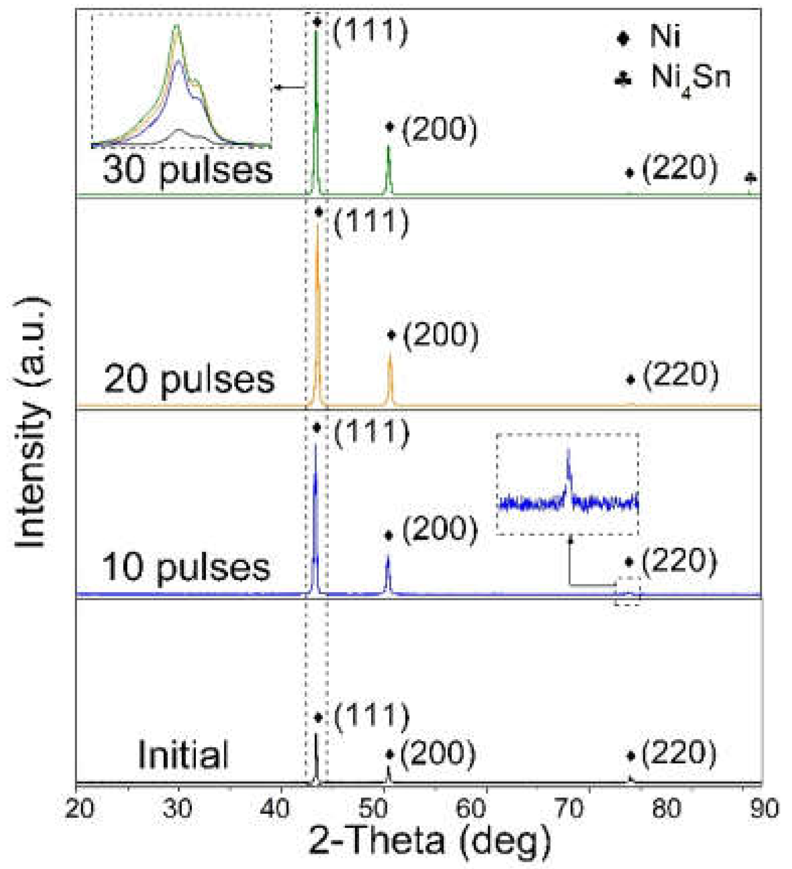
3.1. XRD Patterns
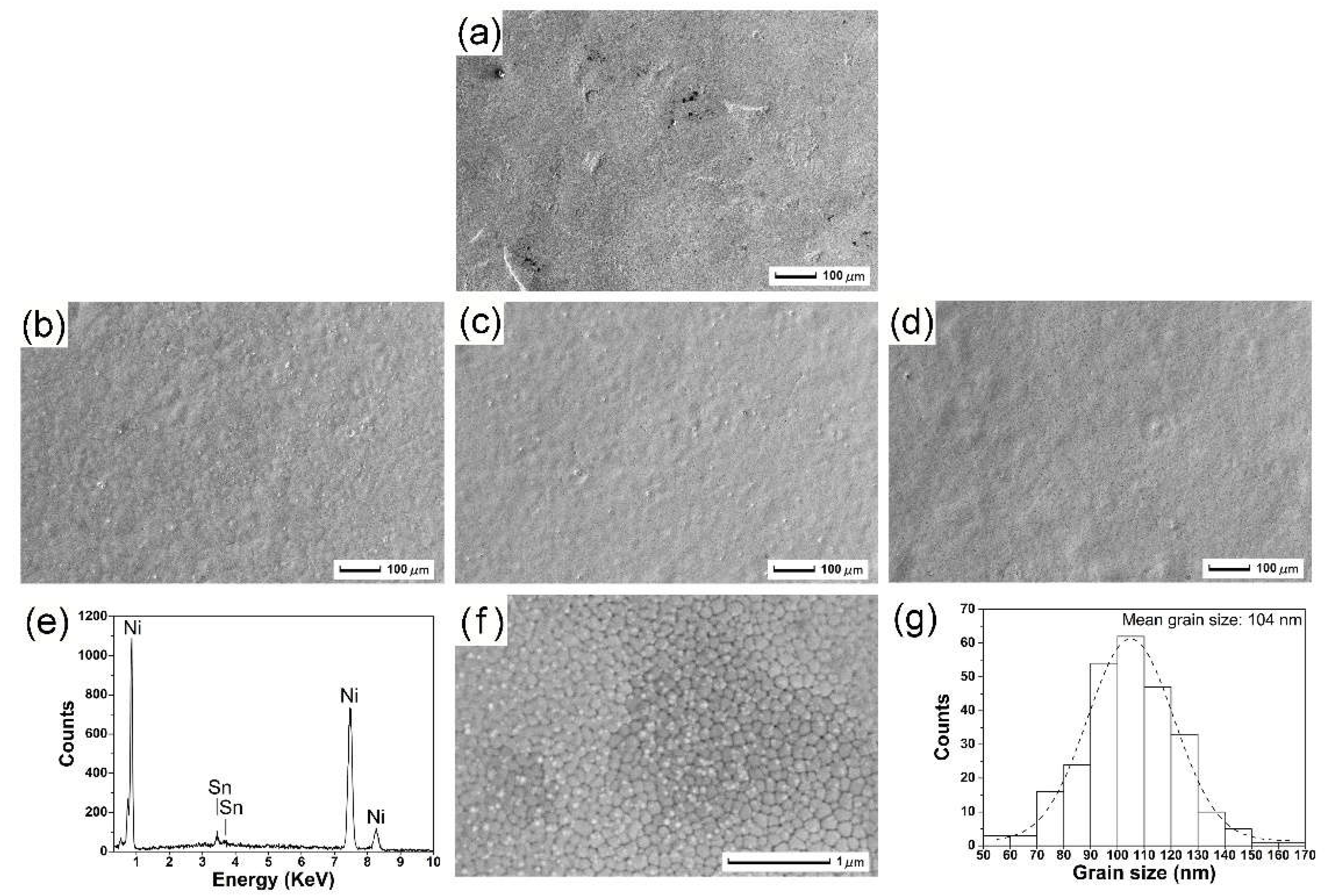
3.2. SEM Characterization
3.3. Hardness Measurements
3.4. VASP
4. Discussion
Author Contributions
Funding
Data Availability Statement
Acknowledgments
Conflicts of Interest
References
- Wu, Y.; Lin, J.; Carlson, B.E.; Lu, P.; Balogh, M.P.; Irish, N.P.; Mei, Y. Effect of laser ablation surface treatment on performance of adhesive-bonded aluminum alloys. Surf. Coat. Tech. 2016, 304, 340–347. [Google Scholar] [CrossRef]
- Xu, J.; Wan, S.; Wang, Y.; Huang, S.; Yuan, Z.; Chen, F.; Zhang, Y.; Liu, T. Enhancing performance of molybdenum doped strontium ferrite electrode by surface modification through Ni infiltration. Int. J. Hydrogen Energ. 2021, 46, 10876–10891. [Google Scholar] [CrossRef]
- Shevchenko, N.; Pham, M.T.; Maitz, M.F. Studies of surface modified NiTi alloy. Appl. Surf. Sci. 2004, 235, 126–131. [Google Scholar] [CrossRef]
- Srichen, A.; Moonngam, S.; Linjee, S.; Banjongprasert, C. Tribological behaviors of arc sprayed NiCrMoAl alloy coating after heat treatments. Surf. Coat. Tech. 2022, 437, 128325. [Google Scholar] [CrossRef]
- Xu, G.; Kutsuna, M.; Liu, Z.; Zhang, H. Characteristics of Ni-based coating layer formed by laser and plasma cladding processes. Mat. Sci. Eng. A 2006, 417, 63–72. [Google Scholar] [CrossRef]
- Borkar, T.; Banerjee, R. Influence of spark plasma sintering (SPS) processing parameters on microstructure and mechanical properties of nickel. Mater. Sci. Eng. A 2014, 618, 176–181. [Google Scholar] [CrossRef]
- Chen, L.; Ren, X.; Zhou, W.; Tong, Z.; Adu-Gyamfi, S.; Ye, Y.; Ren, Y. Evolution of microstructure and grain refinement mechanism of pure nickel induced by laser shock peening. Mater. Sci. Eng. A 2018, 728, 20–29. [Google Scholar] [CrossRef]
- Gavrilov, G.N.; Marinin, E.A.; Yavtushenko, P.M.; Uglov, N.S.; Razheva, K.V. The Study of the Formation Process of Microstructure and Properties during Laser Alloying of the Surface of the Structural Steels. Mater. Sci. Forum. 2021, 1037, 442–448. [Google Scholar] [CrossRef]
- Guo, F.; Jiang, W.; Tang, G.; Xie, Z.; Liu, L. Enhancing anti-wear and anti-corrosion performance of cold spraying aluminum coating by high current pulsed electron beam irradiation. Vacuum 2020, 182, 109772. [Google Scholar] [CrossRef]
- Zhang, L.; Peng, C.-T.; Yao, X.; Guan, Q.; Lu, R. Surface alloying of Cr on Ti6Al4V alloy induced by high-current pulse electron beam. Surf. Coat. Tech. 2019, 370, 288–297. [Google Scholar] [CrossRef]
- Yang, S.; Guo, Z.; Zhao, L.; Guan, Q.; Zhao, L.; Liu, Y. Microstructures and corrosion resistance of Zircaloy-4 after surface alloying with copper by high-current pulsed electron beam. Appl. Surf. Sci. 2020, 501, 144222. [Google Scholar] [CrossRef]
- Zhang, K.M.; Yang, D.Z.; Zou, J.X.; Grosdidier, T.; Dong, C. Improved in vitro corrosion resistance of a NiTi alloy by high current pulsed electron beam treatment. Surf. Coat. Tech. 2006, 201, 3096–3102. [Google Scholar] [CrossRef]
- Peng, L.A.; Tao, P.A.; Ym, A.; Zl, A.; Qi, G.A.; Cz, B.; Yj, C.; Qg, A.; Jie, C.D. Microstructure and properties of CoCrFeNiMo 0.2 high-entropy alloy enhanced by high-current pulsed electron beam. Surf. Coat. Tech. 2021, 410, 126911. [Google Scholar] [CrossRef]
- Yang, S.; Guo, Z.; Zhao, L.; Zhao, L.; Guan, Q.; Liu, Y. Surface microstructures and high-temperature high-pressure corrosion behavior of N18 zirconium alloy induced by high current pulsed electron beam irradiation. Appl. Surf. Sci. 2019, 484, 453–460. [Google Scholar] [CrossRef]
- Zhang, C.; Lv, P.; Cai, J.; Zhang, Y.; Xia, H.; Guan, Q. Enhanced corrosion property of W-Al coatings fabricated on aluminum using surface alloying under high-current pulsed electron beam. J. Alloys Compd. 2017, 723, 258–265. [Google Scholar] [CrossRef]
- Du, X.; Tian, N.; Zhang, C.; Lyu, P.; Cai, J.; Guan, Q. Surface Alloying and Improved Property of Nb on TC4 Induced by High Current Pulsed Electron Beam. Nanomaterials 2021, 11, 2906. [Google Scholar] [CrossRef] [PubMed]
- Kresse, G.; Hafner, J. Ab initio molecular dynamics for liquid metals. Phys. Rev. B 1993, 47, 558–561. [Google Scholar] [CrossRef] [PubMed]
- Perdew, J.P.; Burke, K.; Ernzerhof, M. Generalized Gradient Approximation Made Simple. Phys. Rev. L 1996, 77, 3865–3868. [Google Scholar] [CrossRef] [PubMed] [Green Version]
- Monkhorst, H.J.; Pack, J.D. Special points for Brillouin-zone integrations. Phys. Rev. B 1976, 13, 5188–5192. [Google Scholar] [CrossRef]


| Accelerated Voltage | Current Pulse Duration | Energy Density | Beam Diameter | Pulse Interval | Vacuum |
|---|---|---|---|---|---|
| 27 keV | 1.5 μs | 4 J/cm2 | 60 mm | 8 s | 5 × 10⁻³ Pa |
Publisher’s Note: MDPI stays neutral with regard to jurisdictional claims in published maps and institutional affiliations. |
© 2022 by the authors. Licensee MDPI, Basel, Switzerland. This article is an open access article distributed under the terms and conditions of the Creative Commons Attribution (CC BY) license (https://creativecommons.org/licenses/by/4.0/).
Share and Cite
Zhang, L.; Xu, K.; Liang, T.; Shi, J. Strengthening Analysis of Ni-Sn Alloy Layer by Double Alloying Method Combined with First-Principles Calculation. Nanomaterials 2022, 12, 4127. https://doi.org/10.3390/nano12234127
Zhang L, Xu K, Liang T, Shi J. Strengthening Analysis of Ni-Sn Alloy Layer by Double Alloying Method Combined with First-Principles Calculation. Nanomaterials. 2022; 12(23):4127. https://doi.org/10.3390/nano12234127
Chicago/Turabian StyleZhang, Lingyan, Kai Xu, Tulu Liang, and Jin Shi. 2022. "Strengthening Analysis of Ni-Sn Alloy Layer by Double Alloying Method Combined with First-Principles Calculation" Nanomaterials 12, no. 23: 4127. https://doi.org/10.3390/nano12234127