
Effects of Thermal Annealing on Optical and Microscopic Ferromagnetic Properties in InZnP:Ag Nano-Rods
 , , ,
, , , 
Abstract
:1. Introduction
2. Materials and Methods
3. Results and Discussion
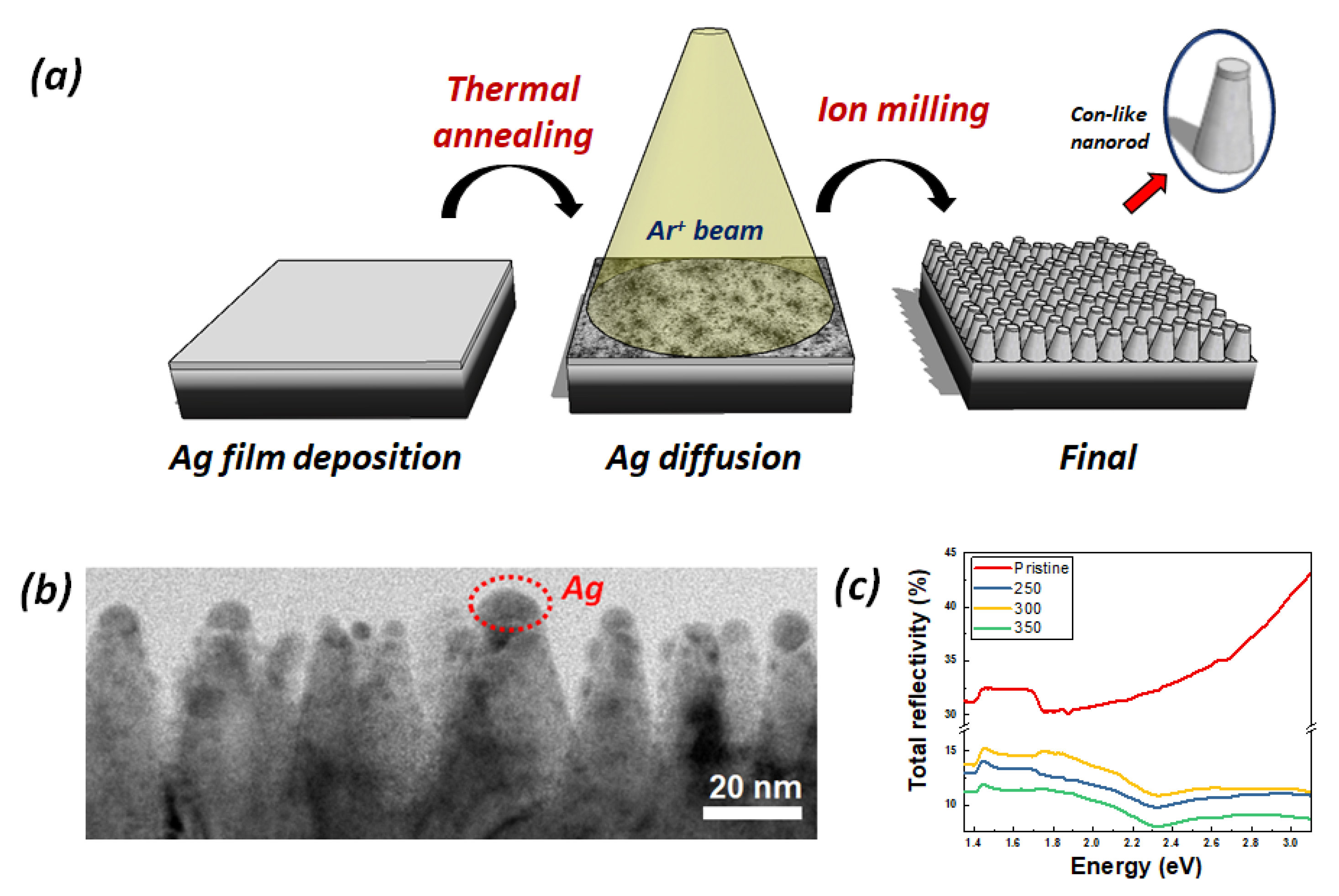
3.1. TEM and Reflectance Spectra
3.2. PL Spectra
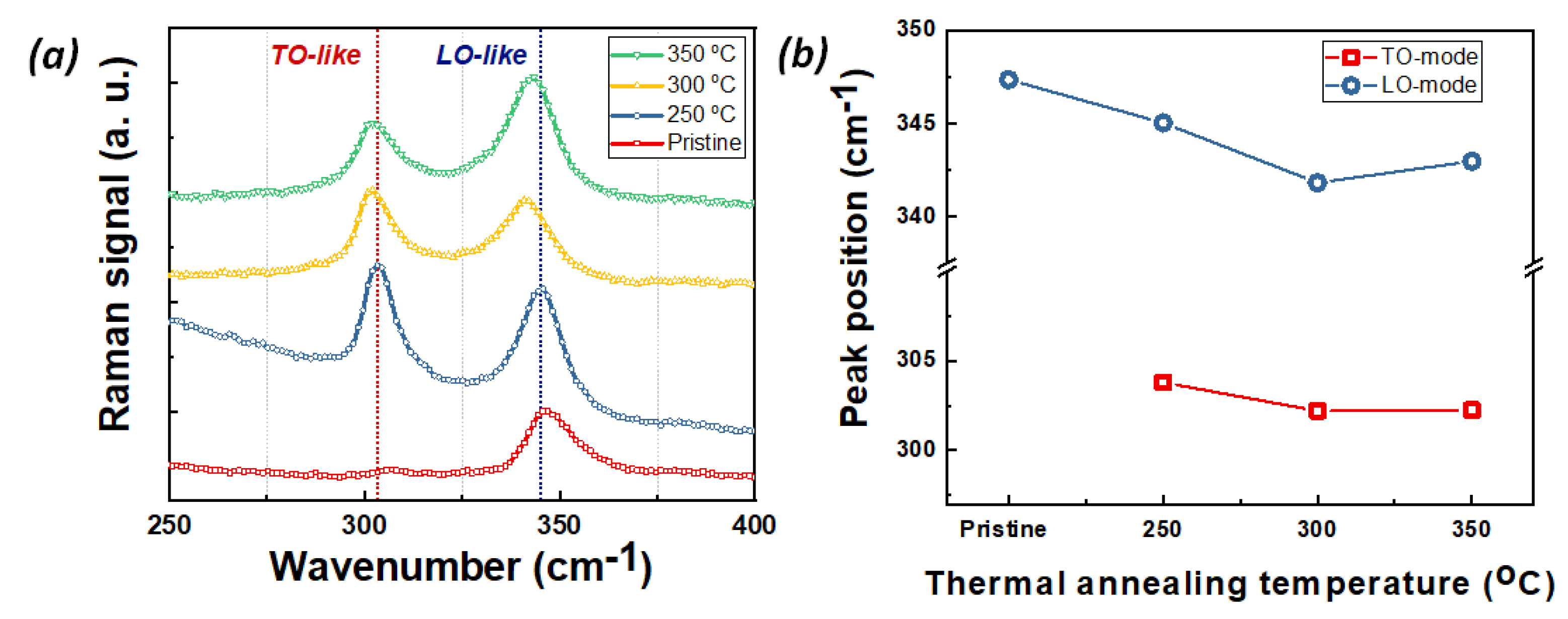
3.3. Raman Spectra
3.4. AFM and MFM
4. Conclusions
Author Contributions
Funding
Institutional Review Board Statement
Informed Consent Statement
Data Availability Statement
Conflicts of Interest
References
- Ohno, H. Making Nonmagnetic Semiconductors Ferromagnetic. Science 1998, 281, 951–956. [Google Scholar] [CrossRef] [PubMed]
- Ohno, H.; Chiba, D.; Matsukura, F.; Omiya, T.; Abe, E.; Dietl, T.; Ohno, Y.; Ohtani, K. Electric-field control of ferromagnetism. Nature 2000, 408, 944–946. [Google Scholar] [CrossRef] [PubMed]
- Dietl, T.; Ohno, H.; Matsukura, F.; Cibert, J.; Ferrand, D. Zener Model Description of Ferromagnetism in Zinc-Blende Magnetic Semiconductors. Science 2000, 287, 1019–1022. [Google Scholar] [CrossRef] [Green Version]
- Hollinger, G.; Gallet, D.; Gendry, M.; Besland, M.P.; Joseph, J. Evidence for a new passivating indium rich phosphate prepared by ultraviolet/ozone oxidation of InP. Appl. Phys. Lett. 1991, 59, 1617. [Google Scholar] [CrossRef]
- Vaccaro, K.; Dauplaise, H.M.; Davis, A.; Spaziani, S.M.; Lorenzo, J.P. Indium phosphide passivation using thin layers of cadmium sulfide. Appl. Phys. Lett. 1995, 67, 527. [Google Scholar] [CrossRef]
- Shon, Y.; Lee, W.C.; Park, Y.S.; Kwon, Y.H.; Lee, S.J.; Chung, K.J.; Kim, H.S.; Kim, D.Y.; Fu, D.J.; Kang, T.W.; et al. Mn-implanted dilute magnetic semiconductor InP:Mn. Appl. Phys. Lett. 2004, 84, 2310. [Google Scholar] [CrossRef]
- Khalid, M.; Weschke, E.; Skorupa, W.; Helm, M.; Zhou, S. Ferromagnetism and impurity band in a magnetic semiconductor: InMnP. Phys. Rev. B 2014, 89, 121301. [Google Scholar] [CrossRef] [Green Version]
- Wang, J.; Gudiksen, M.S.; Duan, X.; Cui, Y.; Lieber, C.M. Highly Polarized Photoluminescence and Photodetection from Single Indium Phosphide Nanowires. Science 2001, 293, 1455–1457. [Google Scholar] [CrossRef] [Green Version]
- Johnson, J.C.; Choi, H.J.; Knutsen, K.P.; Schaller, R.D.; Yang, P.; Saykally, R.J. Single gallium nitride nanowire lasers. Nat. Mater. 2002, 1, 106–110. [Google Scholar] [CrossRef]
- Liang, C.H.; Chen, L.C.; Hwang, J.S.; Chen, K.H.; Hung, Y.T.; Chen, Y.F. Selective-area growth of indium nitride nanowires on gold-patterned Si (100) substrates. Appl. Phys. Lett. 2002, 81, 22. [Google Scholar] [CrossRef]
- Heurlin, M.; Wickert, P.; Fält, S.; Borgström, M.T.; Deppert, K.; Samuelson, L.; Magnusson, M.H. Axial InP Nanowire Tandem Junction Grown on a Silicon Substrate. Nano Lett. 2011, 11, 2028–2031. [Google Scholar] [CrossRef] [PubMed]
- Gambardella, P.; Rusponi, S.; Veronese, M.; Dhesi, S.S.; Grazioli, C.; Dallmeyer, A.; Cabria, I.; Zeller, R.; Dederichs, P.H.; Kern, K.; et al. Giant Magnetic Anisotropy of Single Cobalt Atoms and Nanoparticle. Science 2003, 300, 1130–1133. [Google Scholar] [CrossRef] [PubMed] [Green Version]
- Rodrigues, V.; Bettini, J.; Silva, P.C.; Ugarte, D. Evidence for Spontaneous Spin-Polarized Transport in Magnetic Nanowires. Phys. Rev. Lett. 2003, 91, 096801. [Google Scholar] [CrossRef] [PubMed] [Green Version]
- Cordente, N.; Respaud, M.; Senocq, F.; Casanove, M.J.; Amiens, C.; Chaudret, B. Synthesis and Magnetic Properties of Nickel Nanorods. Nano Lett. 2001, 1, 565–568. [Google Scholar] [CrossRef]
- He, W.; Osmulski, M.E.; Lin, J.; Koktysh, D.S.; McBride, J.R.; Park, J.H.; Dickerson, J.H. Remarkable optical and magnetic properties of ultra-thin europium oxysulfide nanorods. J. Mater. Chem. 2012, 22, 16728–16731. [Google Scholar] [CrossRef]
- Zhou, X.; Zhang, K.H.L.; Xiong, J.; Park, J. Size- and dimensionality-dependent optical, magnetic and magneto-optical properties of binary europium-based nanocrystals: EuX (X = O, S, Se, Te). Nanotechnology 2016, 27, 192001. [Google Scholar] [CrossRef]
- Shen, J.; Wang, C.; Xu, S.; Lv, C.; Zhang, R.; Cui, Y. Joint effect of ferromagnetic and non-ferromagnetic cations for adjusting room temperature ferromagnetism of highly luminescent CuNiInS quaternary nanocrystals. Nanotechnology 2017, 28, 035601. [Google Scholar] [CrossRef]
- Subbarao, U.; Roy, S.; Sarma, S.C.; Sarkar, S.; Mishra, V.; Khulbe, Y.; Peter, S.C. Metal Flux Growth, Structural Relations, and Physical Properties of EuCu2Ge2 and Eu3T2In9 (T = Cu and Ag). Inorg. Chem. 2016, 55, 10351–10360. [Google Scholar] [CrossRef]
- Algra, R.E.; Verheijen, M.A.; Borgström, M.T.; Feiner, L.F.; Immink, G.; Van Enckevort, W.J.P.; Vlieg, E.; Bakkers, E.P.A.M. Twinning superlattices in indium phosphide nanowires. Nature 2008, 456, 369–372. [Google Scholar] [CrossRef] [Green Version]
- Srivastava, P.; Kumar, A.; Jaiswal, N.K. Structural, electronic, and magnetic properties of Mn-Doped InP nanowire. Superlattices Microstruct. 2016, 92, 134–142. [Google Scholar] [CrossRef]
- Schmidt, T.M.P.; Venezuela, P.; Arantes, J.T.; Fazzio, A. Electronic and magnetic properties of Mn-doped InP nanowires from first principles. Phys. Rev. B 2006, 73, 235330. [Google Scholar] [CrossRef]
- Schmidt, T.M. Surface effects on the energetic and spintronic properties of InP nanowires diluted with Mn: First-principles calculations. Phys. Rev. B 2008, 77, 085325. [Google Scholar] [CrossRef]
- Lee, J.; Shon, Y.; Subramaniam, N.G.; Kang, T.; Sohn, J.M.; Kim, H.; Im, H.; Koo, H.C.; Lee, J.H.; Song, J.D.; et al. Magnetic property (Tc~300 K) originated from InZnP:Ag nano-rods fabricated with noble metal Ag using ion milling method. J. Alloys Compd. 2017, 70, 552–556. [Google Scholar] [CrossRef]
- Arnold, G.W.; Borders, J.A. Aggregation and migration of ion-implanted silver in lithia-alumina-silica glass. J. Appl. Phys. 1977, 48, 1488. [Google Scholar] [CrossRef]
- Vinokurov, A.; Chernysheva, G.; Mordvinova, N.; Dorofeev, S. Optical properties and structure of Ag-doped InP quantum dots prepared by a phosphine synthetic route. Dalt. Trans. 2018, 47, 12414–12419. [Google Scholar] [CrossRef] [PubMed]
- Lee, Y.J.; Kim, Y.; Hong, S.; Kwon, S.H. Ultrathin Submicrometer Scale Multicolor Detector of Visible Light Based on Metamaterial. Sensors 2019, 19, 4103. [Google Scholar] [CrossRef] [Green Version]
- Shon, Y.; Lee, S.; Kim, D.Y.; Kang, T.W.; Yoon, C.S.; Kim, E.K.; Lee, J.J. The structural, optical and magnetic properties and anomalous Hall effect of InMnP:Zn epilayers. New J. Phys. 2008, 10, 115002. [Google Scholar] [CrossRef]
- Zakaria, R.; Hamdan, K.S.; Noh, S.M.C.; Supangat, A.; Sookhakian, M. Surface plasmon resonance and photoluminescence studies of Au and Ag micro-flowers. Opt. Mater. Express 2015, 5, 943–950. [Google Scholar] [CrossRef] [Green Version]
- Lee, S.; Song, E.B.; Wang, K.L.; Yoon, C.S.; Yoon, I.T.; Shon, Y.; Kang, T.W. Thermodynamic Behavior of Excitonic Emission Properties in Manganese- and Zinc-Codoped Indium Phosphide Diluted Magnetic Semiconductor Layers. J. Phys. Chem. C 2011, 115, 23564–23567. [Google Scholar] [CrossRef]
- Varshini, Y.P. Temperature dependence of the energy gap in semiconductors. Physica 1967, 34, 149–154. [Google Scholar] [CrossRef]
- Tian, S.; Wei, Z.; Li, Y.; Zhao, H.; Fang, X.; Tang, J.; Fang, D.; Sun, L.; Liu, G.; Yao, B.; et al. Surface state and optical property of sulfur passivated InP. Mater. Sci. Semicond. Process 2014, 17, 33–37. [Google Scholar] [CrossRef]
- Tiginyanu, I.M.; Irmer, G.; Monecke, J.; Hartnagel, H.L. Micro-Raman-scattering study of surface-related phonon modes in porous GaP. Phys. Rev. B 1997, 55, 6739. [Google Scholar] [CrossRef]
- Seong, M.J.; Mićić, O.I.; Nozik, A.J.; Mascarenhas, A.; Cheong, H.M. Size-dependent Raman study of InP quantum dots. Appl. Phys. Lett. 2003, 82, 185. [Google Scholar] [CrossRef]
- Ferri, F.A.; Pereira-Da-Silva, M.A.; Zanatta, A.R. Evidence of magnetic vortices formation in Mn-based sub-micrometre structures embedded in Si–Mn films. J. Phys. D Appl. Phys. 2009, 42, 132002. [Google Scholar] [CrossRef] [Green Version]
- Lide, D.R. CRC Handbook of Chemistry and Physics, 86th ed.; Taylor & Francis: New York, NY, USA, 2005. [Google Scholar]
- Nečas, D.; Klapetek, P.; Neu, V.; Havlíček, M.; Puttock, R.; Kazakova, O.; Hu, X.; Zajíčková, L. Determination of tip transfer function for quantitative MFM using frequency domain filtering and least squares method. Sci. Rep. 2019, 9, 3880. [Google Scholar] [CrossRef] [PubMed] [Green Version]
- Schneider, J.; Kaufmann, U.; Wilkening, W.; Baeumler, M.; Köhl, F. Electronic structure of the neutral manganese acceptor in gallium arsenide. Phys. Rev. Lett. 1987, 59, 240. [Google Scholar] [CrossRef]
- Szczytko, J.; Twardowski, A.; Świątek, K.; Palczewska, M.; Tanaka, M.; Hayashi, T.; Ando, K. Electron paramagnetic resonance studies on Mn doped GaSb. Phys. Rev. B 1999, 60, 8304. [Google Scholar] [CrossRef]


Publisher’s Note: MDPI stays neutral with regard to jurisdictional claims in published maps and institutional affiliations. |
© 2022 by the authors. Licensee MDPI, Basel, Switzerland. This article is an open access article distributed under the terms and conditions of the Creative Commons Attribution (CC BY) license (https://creativecommons.org/licenses/by/4.0/).
Share and Cite
Lee, J.; Shon, Y.; Kwon, Y.; Kyhm, J.-H.; Kim, D.Y.; Kang, J.H.; Park, C.-S.; Lee, K.S.; Kim, E.K. Effects of Thermal Annealing on Optical and Microscopic Ferromagnetic Properties in InZnP:Ag Nano-Rods. Nanomaterials 2022, 12, 4200. https://doi.org/10.3390/nano12234200
Lee J, Shon Y, Kwon Y, Kyhm J-H, Kim DY, Kang JH, Park C-S, Lee KS, Kim EK. Effects of Thermal Annealing on Optical and Microscopic Ferromagnetic Properties in InZnP:Ag Nano-Rods. Nanomaterials. 2022; 12(23):4200. https://doi.org/10.3390/nano12234200
Chicago/Turabian StyleLee, Juwon, Yoon Shon, Younghae Kwon, Ji-Hoon Kyhm, Deuk Young Kim, Joon Hyun Kang, Chang-Soo Park, Kyoung Su Lee, and Eun Kyu Kim. 2022. "Effects of Thermal Annealing on Optical and Microscopic Ferromagnetic Properties in InZnP:Ag Nano-Rods" Nanomaterials 12, no. 23: 4200. https://doi.org/10.3390/nano12234200