Abstract
In this work, an AlGaN-based Deep-Ultraviolet Light-Emitting Diode structure has been designed and simulated for the zincblende and wurtzite approaches, where the polarization effect is included. DFT analysis was performed to determine the band gap direct-to-indirect cross-point limit, AlN carrier mobility, and activation energies for p-type dopants. The multiple quantum wells analysis describes the emission in the deep-ultraviolet range without exceeding the direct-to-indirect bandgap cross-point limit of around 77% of Al content. Moreover, the quantum-confined Stark effect on wavefunctions overlapping has been studied, where Al-graded quantum wells reduce it. Both zincblende and wurtzite have improved electrical and optical characteristics by including a thin AlGaN with low Al content. Mg and Be acceptor activation energies have been calculated at 260 meV and 380 meV for Be and Mg acceptor energy, respectively. The device series resistance has been decreased by using Be instead of Mg as the p-type dopant from 3 kΩ to 0.7 kΩ.
1. Introduction
Nowadays, III-nitride is one of the most important semiconductor families for device development, such as transistors, lasers, photodetectors, and light-emitting diodes (LEDs) [1]. Different approaches have been developed to emit light in the Deep-Ultraviolet range, under 280 nm, in order to obtain high efficiency and substitute low-pressure mercury lamps [2]. A special effort has been made to determine the ultraviolet susceptibility of different viruses such as SARS-CoV-2, MERS-CoV, and Ebola [3,4]. Here, AlGaN-based deep ultraviolet light emitting diodes (DUV-LEDs) are the current approaches for developing germicidal radiation devices [5]. DUV-LEDs have been developed using nitrides [1,6] due to the wide bandgap [7] and different advantages such as low power, small size with higher efficiency, and wavelength tunability [8]. Nanostructures, nitride-based alloys [9], quantum barrier structures such as graded quantum barriers [10], and quantum wells [11] have been studied to emit in the DUV range, improving the efficiency. Recently, also micro-LEDs have been explored [12,13], resulting in the device size reduction by a light extraction improvement [14].
It is remarkable to mention that, despite external quantum efficiency (EQE) remaining under 10% [15,16,17], some works have overcome this limit. This improvement is commonly performed by considering mirror electrodes, p-AlGaN contact layer instead of typical p-GaN, and high reflective photonic crystal on the p-AlGaN contact layer [18,19]. In general, two different crystal phases to grow III-Nitride semiconductors are explored: hexagonal (wurtzite) and cubic (zincblende) phases [7], while for deep-ultraviolet (DUV) LEDs development, several considerations must be taken into account [20]. On the other hand, wurtzite (wz) materials allow for the incorporation of higher Al concentration to emit in the DUV range in comparison with zincblende (zb) alternative due to the cross-point limit of around 70% of Al in zb-AlGaN-based [7,21]. Commonly, the nanostructures on sapphire substrates have been widely studied [22,23]. However, the limitations of the strong piezoelectric fields attributed to hexagonal semiconductors [24] drive to cubic phase as an essential alternative in III-nitride DUV-LED development. The first consideration is to decrease the effects of intense piezoelectric and spontaneous polarization in the hexagonal phase [25] by substituting it with zb-AlGaN ternary alloy.
Furthermore, recently cubic phase has demonstrated the capability to achieve high hole concentration due to its lower activation energy ~100 meV for p-dopant Mg in zb-GaN. [26] If the hole activation energy is reduced, zb-AlGaN improves DUV-LEDs’ efficiency by reducing optical absorptions in the p-AlGaN contact layer [27]. Therefore, in this work, we start our study by analyzing the bandgap cross-point limit in zb-AlGaN, the Mg, and Be doping for Al content under the direct-to-indirect bandgap cross-point limit by Density Functional Theory (DFT) to be employed in a DUV-LED. Then, once simulated, a discussion on the potential to emit in the germicidal range for the zb-AlGaN approach is performed, focused on Be as p-type doping and its effect on LED performance.
2. Theory and Calculations
2.1. DFT Calculations
It is critical to focus on the p-doping performance of zb-AlGaN since it is essential to achieving zb-AlGaN-based DUV-LED and other optoelectronic devices. Figure 1 shows the atomic structure of zb-Al0.7Ga0.3N with p-type substituting dopant (Be or Mg) considered for simulation to obtain the activation energy for the dopants.
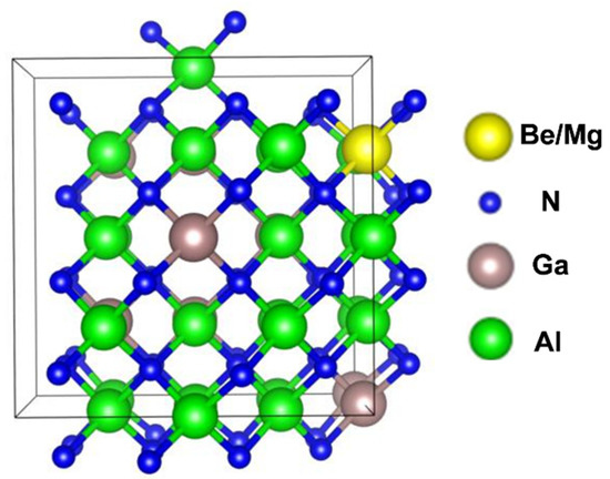
Figure 1.
Schematics of the atomic structure of zb-AlGaN with substitute dopant Be/Mg for DFT calculations.
The substituting Be and Mg defect formation energy as a function of the Fermi level calculated under N-rich conditions are shown in Figure 2a,b, respectively. Our previous work has shown that in zb-GaN, the Mg acceptor possesses a shallow activation energy level at 100 meV and formation energy of about 1.2 Ev [26].
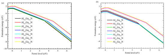
Figure 2.
Formation energy of doped AlGaN with (a) Be and (b) Mg.
In zb-AlGaN nitride, it is observed that the activation energy for Mg increases with Al content and ranges from 150 meV in zb-Al0.2Ga0.8N to 370 meV in zb-Al0.8Ga0.2N, which is lower (Figure 3) compared to the wz-AlGaN:Mg [28].
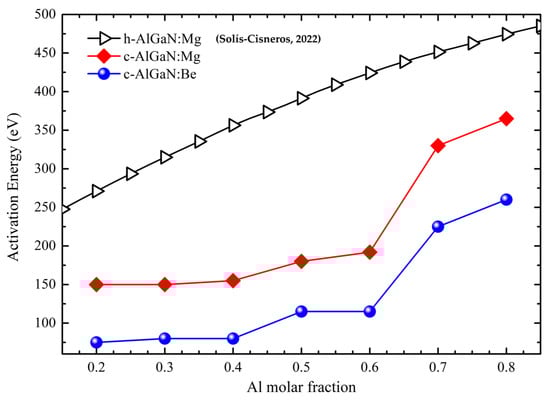
Figure 3.
Activation energy comparison between zb- and wz- AlGaN doped with Mg and Be, see ref. [20].
This behavior shows that Mg remains a shallow acceptor in zb-AlGaN. As a main group-II element, Be is also expected to act as an effective p-type dopant by substituting Al or Ga, though no experiment has proven it until now. Compared to Mg, Be in zb-AlGaN shows higher formation energy but lower activation energy which ranges from 75 meV in zb-Al0.2Ga0.8N to 260 meV in zb-Al0.8Ga0.2N. Such shallow activation energy is consistent with previous work [29] and demonstrates that Be is suitable as a p-type dopant in zb-AlGaN. The formation energy of Be as a substitute dopant is higher than Mg due to the larger mismatched atomic radius between Be and Al/Ga. Like Mg, Be in zb-AlGaN also shows an increasing activation energy level with increasing Al content. The effective mass approximation model can explain this. The activation energy is approximated as Coulombic attraction energy between an electron and a nucleus charge similar to a hydrogen atom: [30] (m*e4)/(32π2ε2ħ2), where m* is the effective mass, e is the elementary charge, and ε is the dielectric constant. Since GaN has a larger dielectric constant but similar effective mass for holes (compared to AlN), the activation energy of Mg and Be in GaN is smaller and would increase when more Al content is included.
In the context of DUV-LED application, the direct band gap of the active materials should be ~4.8 eV. The zb-GaN has a direct bandgap of 3.2 eV, and zb-AlN shows an indirect bandgap of 5.0–5.3 or even 6.0 eV considering the conduction band edge at Γ-valley for indirect-gap alloys [31]. Thus, incorporating Al into GaN can modulate the bandgap and achieve a 4.8 eV bandgap requirement. However, for alloy zb-AlxGa1-xN, the bandgap could transition from a direct to an indirect gap as x increases. Therefore, the Al content limit is critical information for materials and device design, while AlxGa1-xN maintains a direct bandgap. To answer this question, we have performed a DFT calculation to model the band structures of zb-AlxGa1-xN under various x values, as shown in Figure 4a. Four different Al content levels, 0.7, 0.75, 0.8, 0.85, were studied. It can be seen that zb-Al0.70Ga0.30N presents a direct bandgap while zb-Al0.85Ga0.15N exhibits an indirect bandgap due to the conduction band minimum (CBM) shift from Γ point to X point. Note that the actual band gap values are underestimated for zb-AlxGa1-xN, which corresponds to a well-known DFT limitation. Nonetheless, the band features, such as the direct/indirect gap predicted here, are pretty accurate. Further data interpolation (Figure 4b) reveals that the direct–indirect band crossing occurs at x = 0.77 (Al0.77Ga0.23N), exhibiting a maximum Al content around 0.77, which is valuable guidance to design zb-AlxGa1-xN based DUV range LED and other optoelectronic devices.
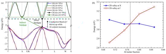
Figure 4.
(a) Crosspoint interpretation from E-K diagram, (b) direct-to-indirect cross-point for zb-AlGaN.
2.2. LED Structure
Binary Compounds Parameters
Besides the direct-to-indirect cross-point limit, the AlN effective masses and carrier mobilities were calculated by DFT. Binary AlN and GaN values were used to establish a cubic III-nitrides-based alloy simulation set. The zb-LED structure () has been approximated by Vegard’s law (Equation (1)) from zb-GaN and zb-AlN parameters shown in Table 1.
where P is the parameter to determine, x is the Al content in the alloy, and b is the bowing factor. Excluding the Energy gap (Eg), all bowings factors were not considered, assuming linear dependency on the Al molar fraction. Moreover, the electron affinity has been calculated using the bandgap offset of 0.75 from ΔEc/(ΔEc + ΔEv) [31]. The zb-AlGaN LEDs have been simulated and studied by analyzing the Power Spectral Density and Current-Voltage (I-V) curves obtained from numerical simulation in SILVACO Atlas, meshing the structure and solving using a finite-element approach. Meshing the structure allows exploring graded profiles with a constant approach to defining nodes inside the region with graded composition.

Table 1.
Parameters to obtain ternary zb-AlGaN.
Capture-Scape rates are simulated to present the influence on the active region of the polarization effect. For SILVACO simulation, the Kronig–Penney model for drift-diffusion, Fermi–Dirac for carrier statistics considering incomplete ionization, and the two-band zb model for gain and radiative recombination have been chosen. For zb and wz-approaches, the radiative recombination dependent on polarization (TE, TM) and spontaneous emission rate are modeled using Equation (2).
where υ is the polarization, nr is the material refractive index, is a polarization-dependent bulk momentum matrix element, fc and fv are the fermi functions in conduction and valence band, m0 is the electron mass in kg, ε0 is the vacuum permittivity, and mr is reduced effective mass obtained from Equation (3).
where mc and mv are effective masses in the conduction and valence band, respectively, this reduced effective mass is used to calculate ρr, the density of states given by Equation (4).
The scaling factor of polarization is set to zero for the zb approach and 1.0 for wz to add the polarization effect. Moreover, for the strain models for zb and wz, strain tensor calculations are performed in the SILVACO environment by selecting the strained two- and three-band models (zb and wz, respectively) for gain and radiative recombination. Before SILVACO simulation, a finite square well analysis based on effective mass approximation was performed. The first energy level in the quantum well (QW) is calculated by solving the Schrödinger Equation, ensuring wavefunction continuity across the entire quantum well/quantum barrier (QW/QB) heterostructure. Energy is calculated using the Newton–Raphson numerical method to solve Equation (5) [35].
where , and are described in Equations (6) and (7), respectively. The variable is the width of the QW in meters, is the barrier height in eV, and is the effective mass in the QW region. This idealized approach has reduced the simulations required in SILVACO to evaluate the structure by narrowing the Al molar fraction and layer thickness ranges.
This quick analysis has been performed to determine a big picture of the thickness and the Al molar fraction in the QW necessary to emit in the DUV range.
The structure to simulate using SILVACO Atlas (Figure 5) was determined by combining DFT restrictions on the maximum Al molar fraction in the zb-AlGaN alloy and the QW width effect on the emission. First, the active region is set as an undoped Al55Ga0.42N/Al0.75Ga0.25N multiple quantum well (MQW) with three QWs to emit around 275 nm with the zb-AlGaN approach. A thin contact layer (P1) has been implemented to mitigate the low light extraction efficiency due to the high transverse-magnetic polarized light dominance in high Al-rich AlGaN-based MQW structures [36]. The hole injection layer (P2) has been proposed as a 30 nm p-Al0.50Ga0.50N with p = 2 × 1019 cm−3. The electron blocking layer (EBL) was considered with p = 2 × 1019 cm−3 [10,37], lower than the GaN:Mg saturation limit [26,38], and an Al molar fraction of 0.75. For comparison to typical hole concentration, simulations with 5 × 1018 cm−3 [39] were also performed. The EBL has been explored under the Al molar fraction, avoiding the direct-to-indirect cross-point limit determined by DFT calculations. Finally, the N-layer consists of 500 nm n-Al0.70Ga0.50N with electron concentration n = 2 × 1019 cm−3 to broaden the electric field along the active region.
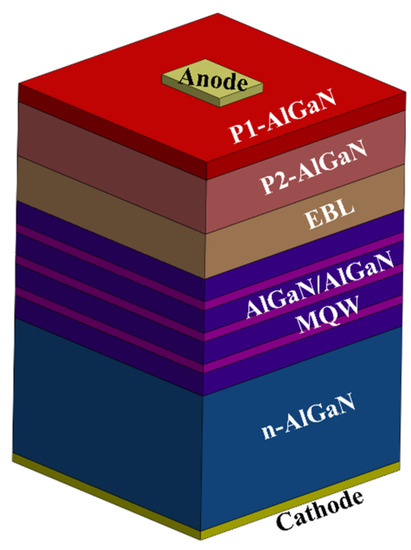
Figure 5.
Purposed LED structure.
3. Results and Discussion
From the data in Figure 1, it can be seen that there is a remarkable reduction in activation energy in the p-layer by doping with Be instead of Mg. DFT calculations for zb Mg doping simulation presented an activation energy of 340 meV for p-Al0.70Ga0.30N, whereas the Be doping shows a lower activation energy of around 200 meV. As shown in Figure 4b, from DFT calculations, the direct bandgap cross-point limit lies at around 0.77 of the Al molar fraction into the AlGaN alloy, consistent with previously reported first-principles [7] and in good agreement with hybrid functional DFT calculations [21]. It would be informative to shed light on the fundamental direct–indirect bandgap transition in AlGaN. For AlGaN, regardless of the Al content, its valence band maximum always stands at Γ point. On the other hand, the conduction band minimum can be either at X or Γ point, depending on their relative energy positions. As Al content increases, the band energy at X gradually decreases, whereas the band energy at Γ gradually increases. This is consistent with the directness feature in AlGaN alloy: at lower Al content, CBM is located at Γ point, so the bandgap is direct; at higher Al content, CBM is at X point, and the bandgap is indirect. The phenomenon that AlN tends to form an indirect gap while GaN tends to have a direct bandgap can be explained by the s-d and p-d orbital interaction [40]. AlN has no d-orbital in Al, so AlN shows an indirect bandgap, similar to Silicon. In GaN, due to the occupied d-orbital in Ga, the s-d and p-d orbital couplings push the conduction band energy at X valley up but leave the Γ valley intact. The calculated direct bandgap cross-point limit provides essential material information for AlGaN-based device design.
In addition to band gap directivity and p-doping capability, carrier mobility is another figure of merit for the AlGaN LED device application. Figure 6 presents the calculated mobilities as a function of doping concentration for both electrons and holes in GaN and AlN. The non-doping limit mobility is limited by phonon scattering [26]. As the doping concentration increases, the Coulombic scattering from ionized dopants increases, so carrier mobility decreases. Phonon scattering and ionized impurity Coulombic scattering are the two fundamental carrier scattering factors in bulk films [41]. It can be seen that GaN shows both high electron and hole mobilities across all the doping concentrations due to the higher intrinsic bulk mobility under the non-doping limit. The mobility values of GaN and AlN will set the upper and lower limit for AlGaN, and depending on Al content, mobilities in AlGaN can be either close to AlN or GaN.
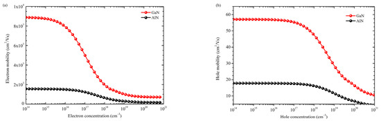
Figure 6.
Zb-approach for the carrier mobility as a function of doping concentration (a) electron and (b) hole in GaN and AlN. The mobility values in GaN and AlN will set the upper the lower limit for carrier mobilities in AlGaN.
The finite square well calculations are shown in Figure 7, indicating the wavelength emissions as a function of QW width for zb-AlGaN-based DUV-LED. It is important to mention that the calculated difference between the analytical finite square well approach and Silvaco numerical simulations lies under 0.1%. So, finite square QW, with the effective mass approach, is quite accurate in predicting the DUV emission range. The zb-AlGaN ideal approximation shows clear access to the DUV range despite the restriction due to the direct-to-indirect cross-point limit. Although zb-QW reaches emission appropriate for surface disinfection, to achieve shorter wavelengths, the QWs thickness requires thinner than the wz-approach. On the other hand, due to intense piezoelectric polarization in the hexagonal crystals, the probability of overlapping electron-hole wavefunctions is reduced, as shown in Figure 8. Overlapping for wz-approach is calculated from the area under the curve of electron and hole wavefunctions as Equation (8). However, in the absence of band distortions, this overlapping has been increased 58. 46% by using the zb approach compared to the wz-structure, and 59.30% using a wz structure with graded QW instead a wz-structure with constant Al molar fraction.
where L is the thickness to integrate, and the min function denotes de overlapping for electron and hole wavefunctions. As the QW thickness increases, the QW emission wavelength also increases due to the thickness dependence of the quantum-confined Stark effect (QCSE). As it is well known, if an electric field is induced in a confined region such as QW, this QCSE provokes a shift in the wavefunctions (electron to the left and holes to de right), reducing the overlapping. This effect has been compensated by grading Al content in each QW (wz- structure with graded QWs) from 0.55 to 0.60 Al molar fraction with a thickness of 1.5 nm [37].
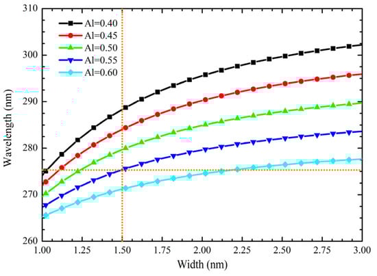
Figure 7.
QW width effect on wavelength of zb-AlGaN-based DUV emission using a single quantum well (SQW) active region.
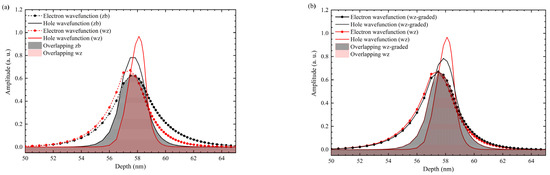
Figure 8.
Overlap of the electron-hole wavefunctions in wz- vs. (a) zb-, and (b) wz-structure with graded QW.
As shown in Figure 9a. the QCSE in the Luminous Power as a function of the QW thickness could be appreciated. Figure 9b presents the electroluminescence shift due to the polarization effect in the QW region, which is mitigated by the zincblende approach. Parameters for simulation are identical in the three simulations neglecting the electric field due to piezoelectric polarization in the zb-approach.
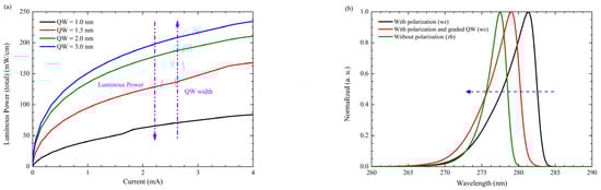
Figure 9.
(a) QCSE in the wz-approach (b) Electroluminescence shift due to polarization in the LED structure as a result of the QCSE.
Figure 10 presents the band diagrams considering the polarization effect. While zb geometry does not show a piezoelectric band distortion, the wz band distortion could be attenuated by grading the Al content in QWs. On the other hand, p-type region presents a slope in the zb approach which is presumably related to the piezoelectric polarization neglected in the model to emulate the zb-approach.
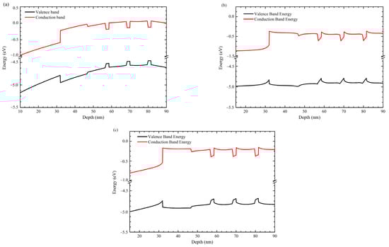
Figure 10.
Band diagrams with 5 V forward bias of (a) zb-, (b) wz-, and (c) wz-structure with graded QWs.
Figure 11a,b shows the carrier concentration due to the polarization effect in three approaches, zb, wz-, and wz- structure with graded QWs structures. By grading the Al content in the QW, the capture electrons concentration diminishes. However, the performance is closer to the zb approach, where electron-hole wavefunctions overlapping increases the direct recombination. Only Mg- and Si-doped P- and N-type layers have been considered, respectively. Nevertheless, current density is improved by substituting Mg with a Be dopant (Figure 11c).
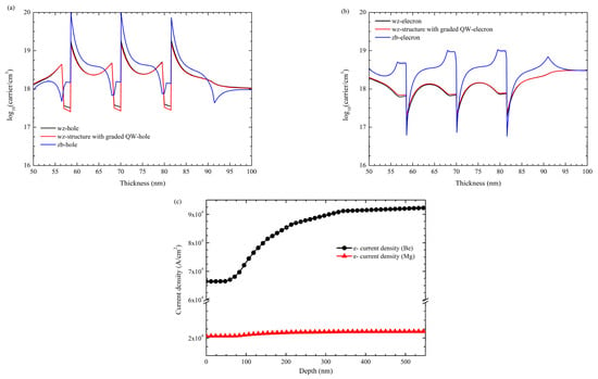
Figure 11.
(a) Electron concentration for zb-, wz-, and wz-structure with graded QW. (b) Hole concentration for zb-, wz-, and wz-structure with graded QW, and (c) electron current density for zb-structure with different p-type dopants.
Additionally, to enhance the electrical characteristics of the DUV-LED, the content of Al in the P1 layer is varied and compared to the structure without the P1 layer and a p-GaN thin contact layer. I-V curves for these simulations are presented in Figure 12, considering incomplete ionization and acceptor activation energy (Figure 2 in Section 2) for Be- and Mg-doping at 260 meV and 370 meV, respectively.
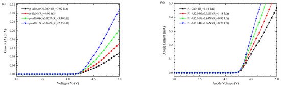
Figure 12.
Effect of P1 contact layer incorporation on RS in the zb-approach using (a) Mg-dopant and (b) Be-dopant.
By selecting Be instead of Mg as a p-type dopant, the Rs of the structure is reduced approximately three times. Figure 13a shows a resistance reduction with the same LED structure and carrier concentrations considering the Mg and Be dopants. Since the p = 2 × 10⁻¹⁹ cm−3 is a technological challenge in Al-rich layers, it is important to mention that epitaxial growth over the p = 2 × 1019 cm−3 has been explored experimentally for the zb-GaN [26] and Mg saturation limit was determined in previous work which points to encourage the experimental research on zb-AlGaN doping for DUV applications.
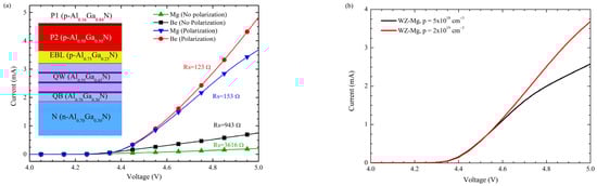
Figure 13.
(a) Rs comparison between the zb-approach (No polarization) and wz-approach (Polarization) for Be and Mg dopants (b) comparison between 5 × 1018 cm−3 and 2 × 1019 cm−3.
4. Conclusions
The simulations show that zb-AlGaN is a candidate for the development of DUV-LED. As presented in this work, a simple approximation, such as SQW, shows that the range of luminescence lies under 275 nm if the QW thickness stands under 1.5 nm and the Al content is limited by the direct-to-indirect cross-point limit of around 77%. Moreover, highly-doped cubic III-nitrides are possible due to their lower activation energy for dopants. The activation energy presented more than 100 meV reduction from 260 to 370 meV using Be instead of Mg. The presented electrical and optical characteristics have been improved for the zb-AlGaN-based LED structure by modifying the p-region modification using a thin AlGaN-based contact layer, where Be, as the p-type dopant, exhibits an LED performance enhancement. A reduction of the Rs from 2.35 kΩ to 0.72 kΩ without the polarization effect in the structure has been determined by considering Be-dopant instead of Mg, presenting Be as an alternative to improve DUV-LED performance by modifying the p-type layers. Moreover, by grading the QW, the polarization effect on bands has been mitigated, enabling future research.
Author Contributions
Conceptualization, H.I.S.-C.; methodology, H.I.S.-C. and Y.H.; software, H.I.S.-C. and Y.H.; validation, H.R.H.-d.-L., Y.H. and C.A.H.-G.; formal analysis, H.I.S.-C., Y.H., H.R.H.-d.-L. and A.-R.A.; investigation, H.I.S.-C., Y.H., R.M.-R. and J.L.C.-A.; resources, H.R.H.-d.-L. and C.A.H.-G.; data curation, A.-R.A., R.G.-C., R.M.-R. and J.L.C.-A.; writing—original draft preparation, H.I.S.-C. and Y.H.; writing—review and editing, R.M.-R., J.L.C.-A. and C.A.H.-G.; visualization, A.-R.A., R.G.-C. and C.A.H.-G.; supervision, C.A.H.-G.; project administration, C.A.H.-G.; funding acquisition, C.A.H.-G. All authors have read and agreed to the published version of the manuscript.
Funding
The APC was funded by Instituto de Ciencia, Tecnología e Innovación del Estado de Chiapas as part of Programa para el Desarrollo de la Investigación Científica, Desarrollo Tecnológico e Innovación 2022.
Data Availability Statement
The data presented in this study are available on request from the corresponding author.
Acknowledgments
Authors thank Instituto de Ciencia, Tecnología e Innovación del Estado de Chiapas for its support. Horacio I. Solís-Cisneros thanks Consejo Nacional de Ciencia y Tecnología in Mexico (CONACYT) for its postgraduate scholarship program.
Conflicts of Interest
The authors declare no conflict of interest. The funders had no role in the design of the study; collection, analyses, or interpretation of data; in the writing of the manuscript; or in the decision to publish the results.
References
- Chen, F.; Ji, X.; Lau, S.P. Recent progress in group III-nitride nanostructures: From materials to applications. Mater. Sci. Eng. R Rep. 2020, 142, 100578. [Google Scholar] [CrossRef]
- Green, A.; Popović, V.; Warriner, K.; Koutchma, T. The efficacy of UVC LEDs and low pressure mercury lamps for the reduction of Escherichia coli O157:H7 and Listeria monocytogenes on produce. Innov. Food Sci. Emerg. Technol. 2020, 64, 102410. [Google Scholar] [CrossRef]
- Eickmann, M.; Gravemann, U.; Handke, W.; Tolksdorf, F.; Reichenberg, S.; Müller, T.H.; Seltsam, A. Inactivation of Ebola virus and Middle East respiratory syndrome coronavirus in platelet concentrates and plasma by ultraviolet C light and methylene blue plus visible light, respectively. Transfusion 2018, 58, 2202–2207. [Google Scholar] [CrossRef] [PubMed]
- Heilingloh, C.S.; Aufderhorst, U.W.; Schipper, L.; Dittmer, U.; Witzke, O.; Yang, D.; Zheng, X.; Sutter, K.; Trilling, M.; Alt, M.; et al. Susceptibility of SARS-CoV-2 to UV irradiation. Am. J. Infect. Control 2020, 48, 1273–1275. [Google Scholar] [CrossRef]
- Heßling, M.; Hönes, K.; Vatter, P.; Lingenfelder, C. Ultraviolet irradiation doses for coronavirus inactivation—Review and analysis of coronavirus photoinactivation studies. GMS Hyg. Infect. Control 2020, 15, Doc8. [Google Scholar] [CrossRef]
- Liu, S.; Luo, W.; Li, D.; Yuan, Y.; Tong, W.; Kang, J.; Wang, Y.; Li, D.; Rong, X.; Wang, T.; et al. Sec-Eliminating the SARS-CoV-2 by AlGaN Based High Power Deep Ultraviolet Light Source. Adv. Funct. Mater. 2021, 31, 2008452. [Google Scholar] [CrossRef]
- Tsai, Y.C.; Bayram, C. Structural and Electronic Properties of Hexagonal and Cubic Phase AlGaInN Alloys Investigated Using First Principles Calculations. Sci. Rep. 2019, 9, 6583. [Google Scholar] [CrossRef]
- Zollner, C.J.; DenBaars, S.P.; Speck, J.S.; Nakamura, S. Germicidal ultraviolet LEDs: A review of applications and semiconductor technologies. Semicond. Sci. Technol. 2021, 36, 123001. [Google Scholar] [CrossRef]
- Amano, H.; Collazo, R.; De Santi, C.; Einfeldt, S.; Funato, M.; Glaab, J.; Hagedorn, S.; Hirano, A.; Hirayama, H.; Ishii, R.; et al. The 2020 UV emitter roadmap. J. Phys. D Appl. Phys. 2020, 53, 503001. [Google Scholar] [CrossRef]
- Yu, H.; Ren, Z.; Zhang, H.; Dai, J.; Chen, C.; Long, S.; Sun, H. Advantages of AlGaN-based deep-ultraviolet light-emitting diodes with an Al-composition graded quantum barrier. Opt. Express 2019, 27, A1544–A1553. [Google Scholar] [CrossRef]
- Du, P.; Shi, L.; Liu, S.; Zhou, S. Polarization-doped quantum wells with graded Al-composition for highly efficient deep ultraviolet light-emitting diodes. Micro Nanostruct. 2022, 163, 107150. [Google Scholar] [CrossRef]
- Yu, H.; Memon, M.H.; Wang, D.; Ren, Z.; Zhang, H.; Huang, C.; Tian, M.; Sun, H.; Long, S. AlGaN-based deep ultraviolet micro-LED emitting at 275 nm. Opt. Lett. 2021, 46, 3271–3274. [Google Scholar] [CrossRef]
- Wong, M.S.; Lee, C.; Myers, D.J.; Hwang, D.; Kearns, J.A.; Li, T.; Speck, J.S.; Nakamura, S.; DenBaars, S.P. Size-independent peak efficiency of III-nitride micro-light-emitting-diodes using chemical treatment and sidewall passivation. Appl. Phys. Express 2019, 12, 97004. [Google Scholar] [CrossRef]
- Tian, M.; Yu, H.; Memon, M.H.; Xing, Z.; Huang, C.; Jia, H.; Zhang, H.; Wang, D.; Fang, S.; Sun, H. Enhanced light extraction of the deep-ultraviolet micro-LED via rational design of chip sidewall. Opt. Lett. 2021, 46, 4809–4812. [Google Scholar] [CrossRef] [PubMed]
- Saifaddin, B.K.; Almogbel, A.S.; Zollner, C.J.; Wu, F.; Bonef, B.; Iza, M.; Nakamura, S.; Denbaars, S.P.; Speck, J.S. AlGaN Deep-Ultraviolet Light-Emitting Diodes Grown on SiC Substrates. ACS Photonics 2020, 7, 554–561. [Google Scholar] [CrossRef]
- Wang, Y.; Rong, X.; Ivanov, S.; Jmerik, V.; Chen, Z.; Wang, H.; Wang, T.; Wang, P.; Jin, P.; Chen, Y.; et al. Deep Ultraviolet Light Source from Ultrathin GaN/AlN MQW Structures with Output Power Over 2 Watt. Adv. Opt. Mater. 2019, 7, 1801763. [Google Scholar] [CrossRef]
- Lee, T.H.; Lee, B.R.; Son, K.R.; Shin, H.W.; Kim, T.G. Highly Efficient Deep-UV Light-Emitting Diodes Using AlN-Based Deep-UV-Transparent Glass Electrodes. ACS Appl. Mater. Interfaces 2017, 9, 43774–43781. [Google Scholar] [CrossRef]
- Takano, T.; Mino, T.; Sakai, J.; Noguchi, N.; Tsubaki, K.; Hirayama, H. Deep-ultraviolet light-emitting diodes with external quantum efficiency higher than 20% at 275 nm achieved by improving light-extraction efficiency. Appl. Phys. Express 2017, 10, 031002. [Google Scholar] [CrossRef]
- Kashima, Y.; Maeda, N.; Matsuura, E.; Jo, M.; Iwai, T.; Morita, T.; Kokubo, M.; Tashiro, T.; Kamimura, R.; Osada, Y.; et al. High external quantum efficiency (10%) AlGaN-based deep-ultraviolet light-emitting diodes achieved by using highly reflective photonic crystal on p-AlGaN contact layer. Appl. Phys. Express 2018, 11, 012101. [Google Scholar] [CrossRef]
- Solís-Cisneros, H.; Hernández-Gutiérrez, C.A.; Anwar, A.-R.; Sevilla-Camacho, P.Y.; Camas-Anzueto, J.L.; Grajales-Coutiño, R.; Trejo-Hernández, R.; Casallas-Moreno, Y.L.; L’ópez-López, M. Physical and technological analysis of the AlGaN-based UVC-LED: An extended discussion focused on cubic phase as an alternative for surface disinfection. Rev. Mex. Fís. 2022, 68, 020301. [Google Scholar] [CrossRef]
- Landmann, M.; Rauls, E.; Schmidt, W.G.; Röppischer, M.; Cobet, C.; Esser, N.; Schupp, T.; As, D.J.; Feneberg, M.; Goldhahn, R. Transition energies and direct-indirect band gap crossing in zinc-blende AlxGa1-xN. Phys. Rev. B 2013, 87, 195210. [Google Scholar] [CrossRef]
- Chen, Z.; Hoo, J.; Chen, Y.; Wang, V.; Guo, S. Study of AlN based materials grown on nano-patterned sapphire substrates for deep ultraviolet led applications. Jpn. J. Appl. Phys. 2019, 58, SC1007. [Google Scholar] [CrossRef]
- Zhao, J.; Hu, H.; Lei, Y.; Wan, H.; Gong, L.; Zhou, S. Heteroepitaxial growth of high-quality and crack-free AlN film on sapphire substrate with nanometer-scale-thick AlN nucleation layer for AlGaN-based deep ultraviolet light-emitting diodes. Nanomaterials 2019, 9, 1634. [Google Scholar] [CrossRef] [PubMed]
- Dakhlaoui, H.; Almansour, S. Piezoelectric polarization and quantum size effects on the vertical transport in AlGaN/GaN resonant tunneling diodes. Chin. Phys. B 2016, 25, 67304. [Google Scholar] [CrossRef]
- Li, X.; Sundaram, S.; Disseix, P.; Gac, G.; Le Bouchoule, S.; Patriarche, G.; Réveret, F.; Leymarie, J.; El Gmili, Y.; Moudakir, T.; et al. AlGaN-based MQWs grown on a thick relaxed AlGaN buffer on AlN templates emitting at 285 nm. Opt. Mater. Express 2015, 5, 380–392. [Google Scholar] [CrossRef]
- Hernández-Gutiérrez, C.A.; Casallas-Moreno, Y.L.; Rangel-Kuoppa, V.-T.; Cardona, D.; Hu, Y.; Kudriatsev, Y.; Zambrano-Serrano, M.A.; Gallardo-Hernandez, S.; Lopez-Lopez, M. Study of the heavily p-type doping of cubic GaN with Mg. Sci. Rep. 2020, 10, 16858. [Google Scholar] [CrossRef] [PubMed]
- Hou, Y.; Guo, Z. Improve the electrical and optical performance of deep ultraviolet light-emitting diodes with a w-shaped p-AlGaN layer. J. Mater. Sci. Mater. Electron. 2019, 30, 7393–7399. [Google Scholar] [CrossRef]
- Zhao, C.-Z.; Wei, T.; Chen, L.-Y.; Wang, S.-S.; Wang, J. The activation energy for Mg acceptor in AlxGa1-xN alloys in the whole composition range. Superlattices Microstruct. 2017, 109, 758–762. [Google Scholar] [CrossRef]
- Tsai, Y.C.; Bayram, C. Mitigate self-compensation with high crystal symmetry: A first-principles study of formation and activation of impurities in GaN. Comput. Mater. Sci. 2021, 190, 110283. [Google Scholar] [CrossRef]
- Miller, D.A.B. Quantum Mechanics for Scientists and Engineers; Cambridge University Press: Cambridge, UK, 2008; ISBN 9780521897839. [Google Scholar]
- Tsai, Y.-C.; Bayram, C. Band Alignments of Ternary Wurtzite and Zincblende III-Nitrides Investigated by Hybrid Density Functional Theory. ACS Omega 2020, 5, 3917–3923. [Google Scholar] [CrossRef]
- The Materials Project Materials Data on GaN by Materials Project. 2020. Available online: https://materialsproject.org/materials/mp-830 (accessed on 12 July 2022).
- Jain, A.; Ong, S.P.; Hautier, G.; Chen, W.; Richards, W.D.; Dacek, S.; Cholia, S.; Gunter, D.; Skinner, D.; Ceder, G.; et al. Commentary: The Materials Project: A materials genome approach to accelerating materials innovation. APL Mater. 2013, 1, 11002. [Google Scholar] [CrossRef]
- The Materials Project Materials Data on AlN by Materials Project. 2020. Available online: https://materialsproject.org/materials/mp-1700 (accessed on 12 July 2022).
- Hernández-Gutiérrez, C.A.; Casallas-Moreno, Y.L.; Cardona, D.; Kudriavtsev, Y.; Morales-Acevedo, A.; Santana-Rodríguez, G.; López-López, M. Cubic phase InxGa1-xN/GaN quantum wells for their application to tandem Solar Cells. In Proceedings of the 2017 IEEE 44th Photovoltaic Specialist Conference (PVSC), Washington, DC, USA, 25–30 June 2017; pp. 670–672. [Google Scholar]
- Wang, W.; Chu, C.; Che, J.; Hang, S.; Shao, H.; Tian, K.; Zhang, Y.; Zhang, Z.-H. Is a thin p-GaN layer possible for making high-efficiency AlGaN-based deep-ultraviolet light-emitting diodes? Opt. Express 2021, 29, 29651–29660. [Google Scholar] [CrossRef]
- Yu, H.; Chen, Q.; Ren, Z.; Tian, M.; Long, S.; Dai, J.; Chen, C.; Sun, H. Enhanced Performance of an AlGaN-Based Deep-Ultraviolet LED Having Graded Quantum Well Structure. IEEE Photonics J. 2019, 11, 8201006. [Google Scholar] [CrossRef]
- Hu, Y.; Hernández-Gutiérrez, C.A.; Solís-Cisneros, H.I.; Santana, G.; Kudriatsev, Y.; Camas-Anzueto, J.L.; López-López, M. Blue luminescence origin and Mg acceptor saturation in highly doped zinc-blende GaN with Mg. J. Alloys Compd. 2022, 897, 163133. [Google Scholar] [CrossRef]
- Sarkar, B.; Washiyama, S.; Breckenridge, M.H.; Klump, A.; Baker, J.N.; Reddy, P.; Tweedie, J.; Mita, S.; Kirste, R.; Irving, D.L.; et al. N- and P-type Doping in Al-rich AlGaN and AlN. ECS Trans. 2018, 86, 25–30. [Google Scholar] [CrossRef]
- Yuan, L.-D.; Deng, H.-X.; Li, S.-S.; Wei, S.-H.; Luo, J.-W. Unified theory of direct or indirect band-gap nature of conventional semiconductors. Phys. Rev. B 2018, 98, 245203. [Google Scholar] [CrossRef]
- Hu, Y.; Hwang, J.; Lee, Y.; Conlin, P.; Schlom, D.G.; Datta, S.; Cho, K. First principles calculations of intrinsic mobilities in tin-based oxide semiconductors SnO, SnO2, and Ta2SnO6. J. Appl. Phys. 2019, 126, 185701. [Google Scholar] [CrossRef]


Publisher’s Note: MDPI stays neutral with regard to jurisdictional claims in published maps and institutional affiliations. |
© 2022 by the authors. Licensee MDPI, Basel, Switzerland. This article is an open access article distributed under the terms and conditions of the Creative Commons Attribution (CC BY) license (https://creativecommons.org/licenses/by/4.0/).