
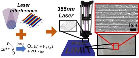
Direct Laser Interference Ink Printing Using Copper Metal–Organic Decomposition Ink for Nanofabrication

 , , , and
Abstract
:
1. Introduction
2. Materials and Methods
2.1. Materials
2.2. Ink Preparation
2.3. Preparation of Substrate
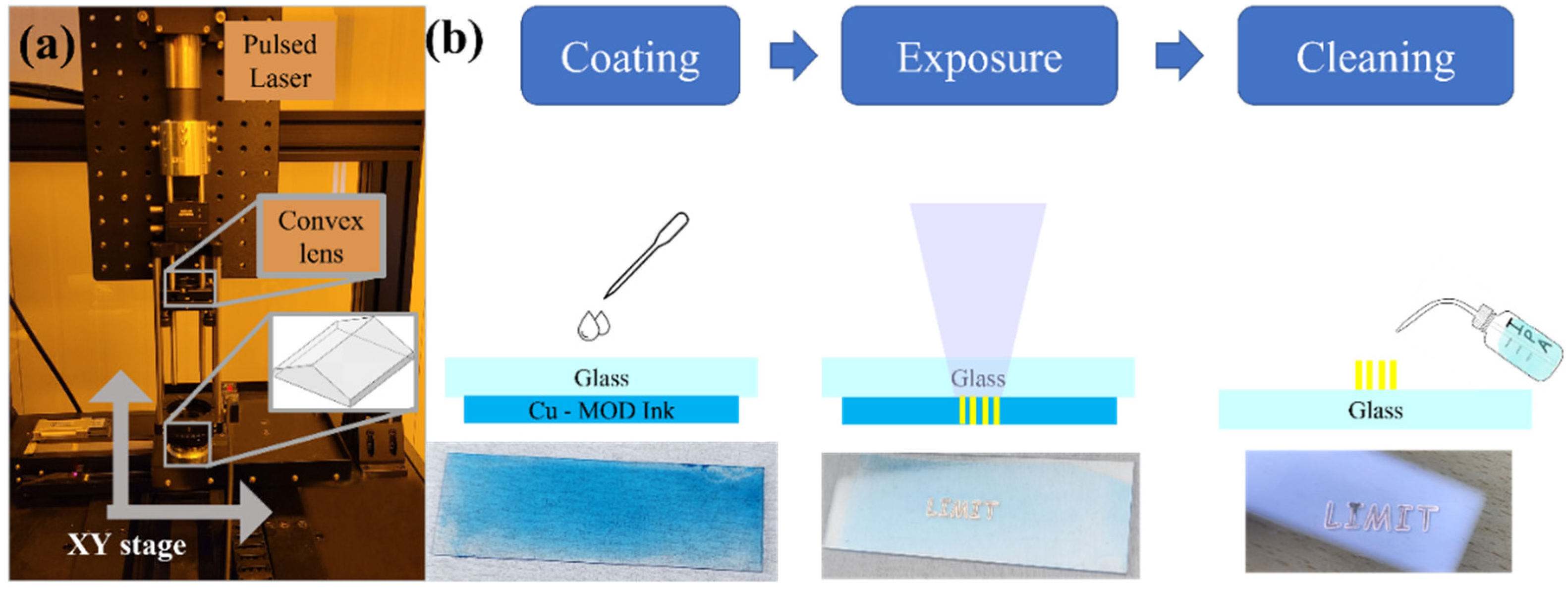
2.4. Laser Irradiation
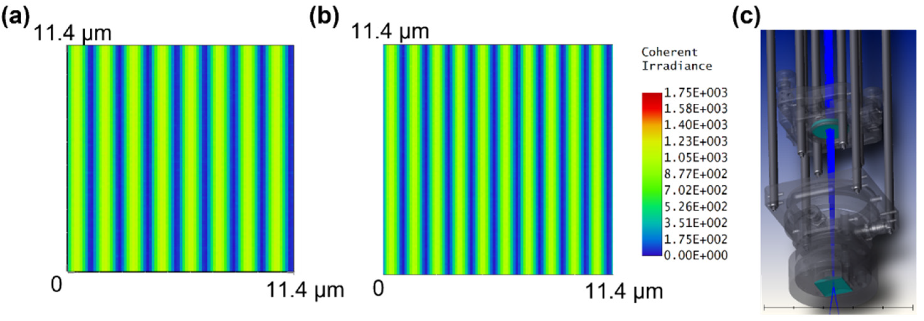
2.4.1. Laser Interference
2.4.2. Laser Interference System
2.5. Methods
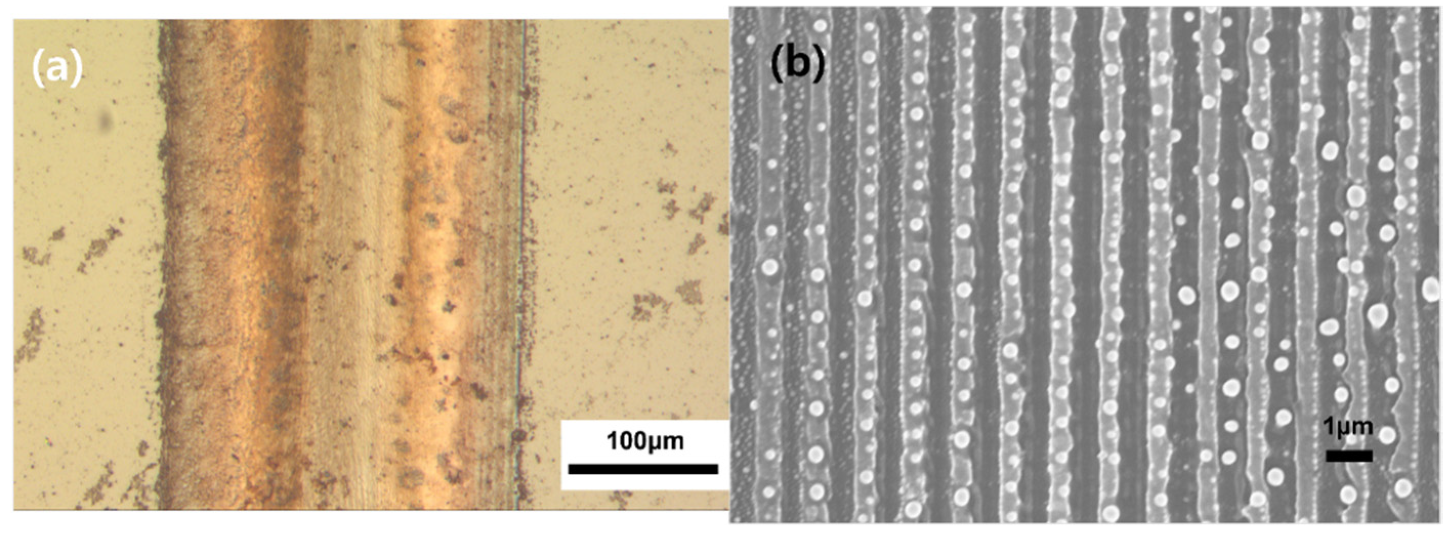
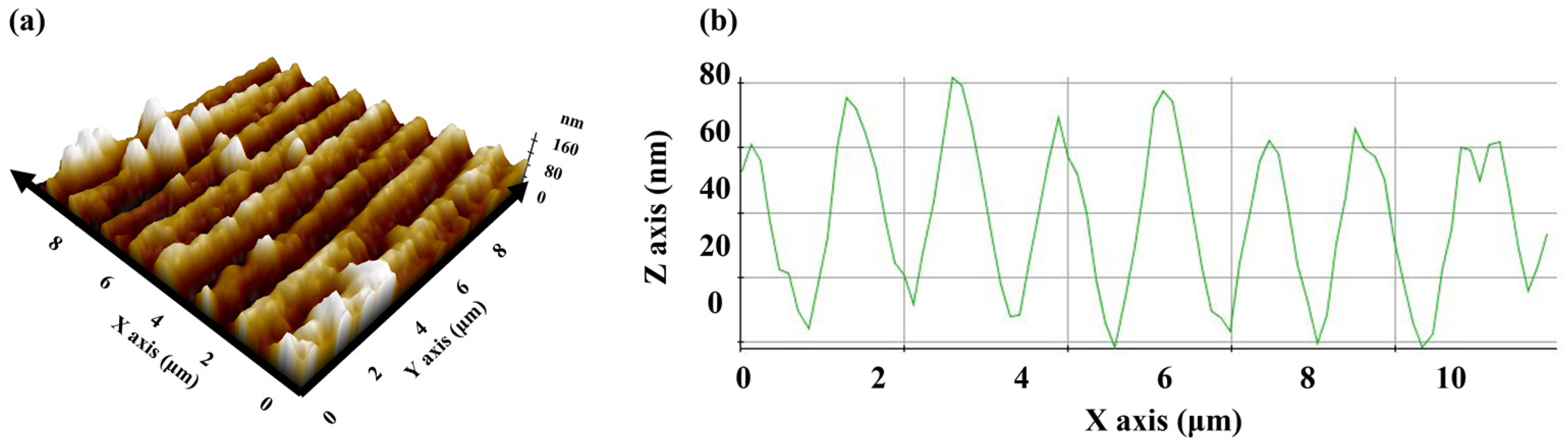
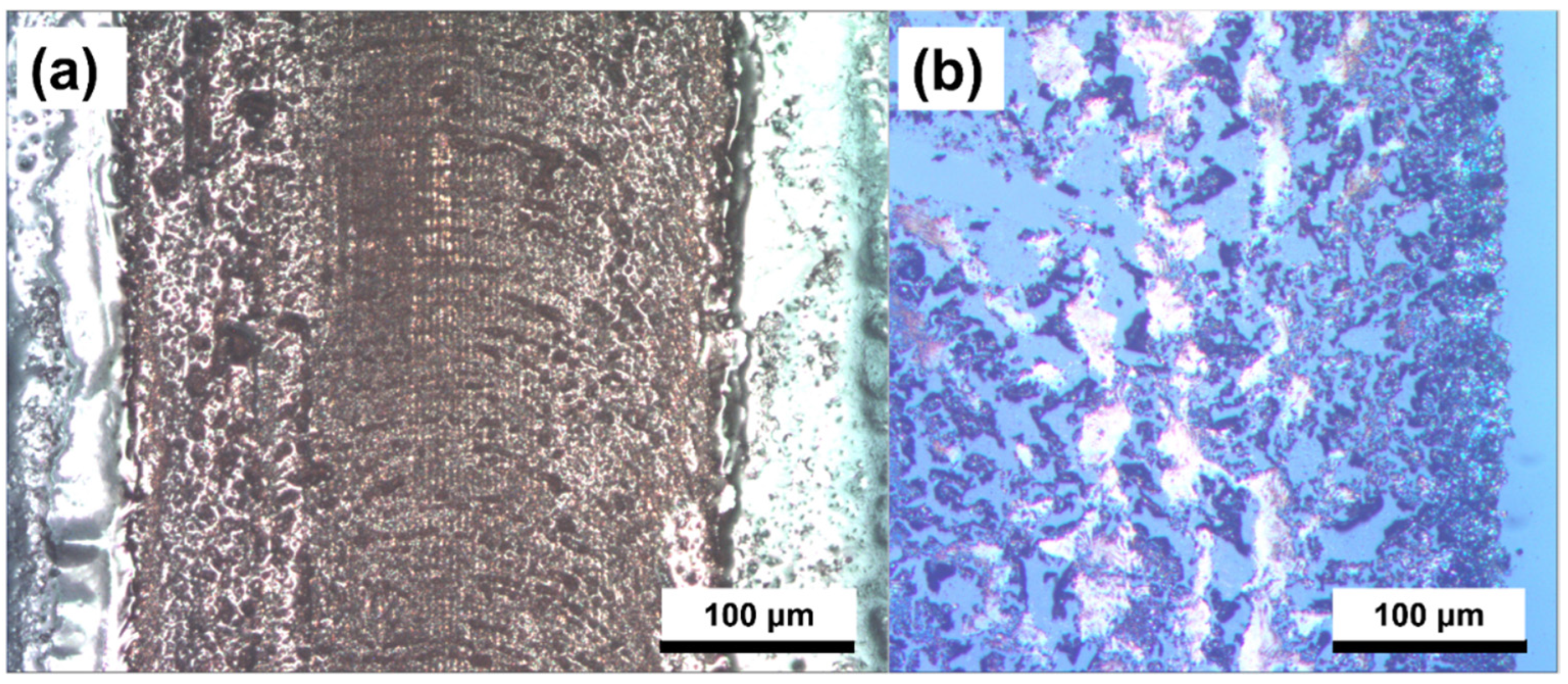
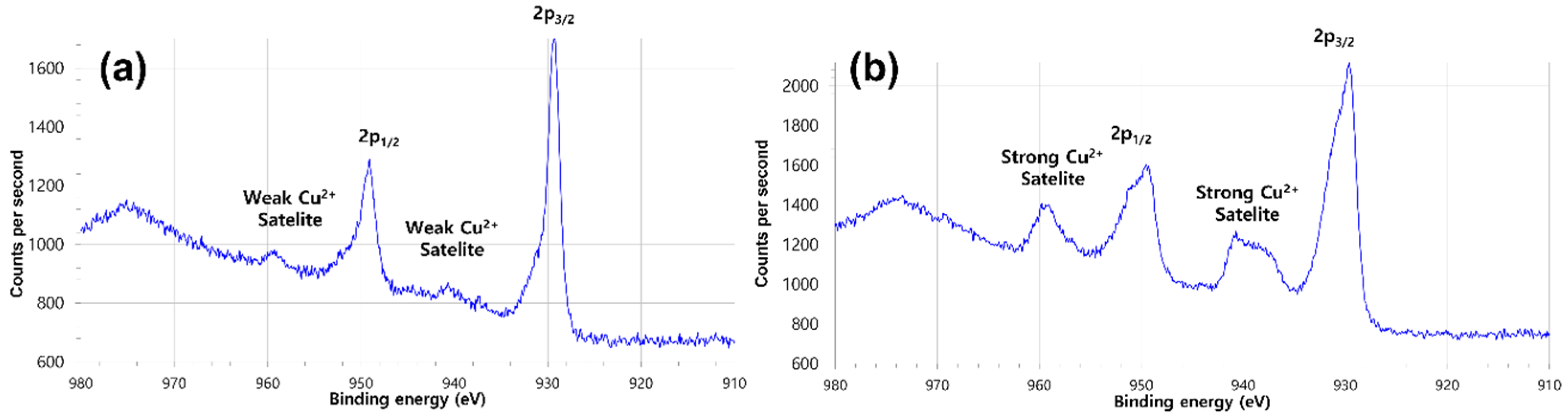
3. Results
4. Conclusions
Supplementary Materials
Author Contributions
Funding
Institutional Review Board Statement
Informed Consent Statement
Data Availability Statement
Conflicts of Interest
References
- Voronin, A.S.; Fadeev, Y.V.; Govorun, I.V.; Podshivalov, I.V.; Simunin, M.M.; Tambasov, I.A.; Karpova, D.V.; Smolyarova, T.E.; Lukyanenko, A.V.; Karacharov, A.A.; et al. Cu–Ag and Ni–Ag meshes based on cracked template as efficient transparent electromagnetic shielding coating with excellent mechanical performance. J. Mater. Sci. 2021, 56, 14741–14762. [Google Scholar] [CrossRef]
- Paeng, D.; Yoo, J.; Yeo, J.; Lee, D.; Kim, E.; Ko, S.H.; Grigoropoulos, C.P. Low-cost facile fabrication of flexible transparent copper electrodes by nanosecond laser ablation. Adv. Mater. 2015, 27, 2762–2767. [Google Scholar] [CrossRef] [PubMed]
- Yoo, J.; Seo, M.; Lee, J.; Choi, K.; Jo, M.; Yoon, J. Industrial grade, bending-insensitive, transparent nanoforce touch sensor via enhanced percolation effect in a hierarchical nanocomposite film. Adv. Funct. Mater. 2018, 28, 1804721. [Google Scholar] [CrossRef]
- Bag, S.; Deneault, J.R.; Durstock, M.F. Aerosol-jet-assisted thin-film growth of CH3NH3PbI3 perovskites—A means to achieve high quality, defect-free films for efficient solar cells. Adv. Energy Mater. 2017, 7, 1701151. [Google Scholar] [CrossRef]
- Correia, V.; Mitra, K.Y.; Castro, H.; Rocha, J.G.; Sowade, E.; Baumann, R.R.; Lanceros-Méndez, S. Design and fabrication of multilayer inkjet-printed passive components for printed electronics circuit development. J. Manuf. Process. 2018, 31, 364–371. [Google Scholar] [CrossRef]
- Kwon, Y.; Lee, Y.; Kim, S.; Lee, K.; Choa, Y. Full densification of inkjet-printed copper conductive tracks on a flexible substrate utilizing a hydrogen plasma sintering. Appl. Surf. Sci. 2017, 396, 1239–1244. [Google Scholar] [CrossRef]
- Jeong, S.; Song, H.C.; Lee, W.W.; Lee, S.S.; Choi, Y.; Son, W.; Kim, E.D.; Paik, C.H.; Oh, S.H.; Ryu, B.-H. Stable aqueous based Cu nanoparticle ink for printing well-defined highly conductive features on a plastic substrate. Langmuir 2011, 27, 3144–3149. [Google Scholar] [CrossRef]
- Jeong, S.; Woo, K.; Kim, D.; Lim, S.; Kim, J.S.; Shin, H.; Xia, Y.; Moon, J. Controlling the thickness of the surface oxide layer on Cu nanoparticles for the fabrication of conductive structures by ink-jet printing. Adv. Funct. Mater. 2008, 18, 679–686. [Google Scholar] [CrossRef]
- Park, B.K.; Kim, D.; Jeong, S.; Moon, J.; Kim, J.S. Direct writing of copper conductive patterns by ink-jet printing. Thin Solid Films 2007, 515, 7706–7711. [Google Scholar] [CrossRef]
- Lee, Y.; Choi, J.; Lee, K.J.; Stott, N.E.; Kim, D. Large-scale synthesis of copper nanoparticles by chemically controlled reduction for applications of inkjet-printed electronics. Nanotechnology 2008, 19, 415604. [Google Scholar] [CrossRef]
- Wang, L.; Liu, J. Pressured liquid metal screen printing for rapid manufacture of high resolution electronic patterns. RSC Adv. 2015, 5, 57686–57691. [Google Scholar] [CrossRef]
- Seong, K.; Kim, J.M.; Kang, J.; Hwang, M.; Lee, C.; Piao, Y. An ultradurable and uniform cu electrode by blending carbon nanotube fillers in copper-based metal–organic decomposition ink for flexible printed electronics. Adv. Mater. Interfaces 2018, 5, 1800502. [Google Scholar] [CrossRef]
- Guo, C.; Yu, Y.; Liu, J. Rapidly patterning conductive components on skin substrates as physiological testing devices via liquid metal spraying and pre-designed mask. J. Mater. Chem. B 2014, 2, 5739–5745. [Google Scholar] [CrossRef] [PubMed]
- Oh, S.; Yang, K.; Byeon, K.; Shin, J.; Kim, Y.; Do, L.; Choi, K.; Lee, H. Various metallic nano-sized patterns fabricated using an Ag ink printing technique. Electron. Mater. Lett. 2012, 8, 485–489. [Google Scholar] [CrossRef]
- Kim, S.; Lee, W.S.; Lee, J.; Park, I. Direct micro/nano metal patterning based on two-step transfer printing of ionic metal nano-ink. Nanotechnology 2012, 23, 285301. [Google Scholar] [CrossRef]
- Efimov, A.; Arsenov, P.; Kornyushin, D.; Lizunova, A.; Volkov, I.; Ivanov, V. Aerosol jet printing of silver lines with a high aspect ratio on a heated silicon substrate. Materials 2020, 13, 730. [Google Scholar] [CrossRef] [Green Version]
- Lu, S.; Zheng, J.; Cardenas, J.A.; Williams, N.X.; Lin, Y.; Franklin, A.D. Uniform and stable aerosol jet printing of carbon nanotube thin-film transistors by ink temperature control. ACS Appl. Mater. Interfaces 2020, 12, 43083–43089. [Google Scholar] [CrossRef]
- Jung, W.; Jung, Y.; Pikhitsa, P.V.; Feng, J.; Yang, Y.; Kim, M.; Tsai, H.; Tanaka, T.; Shin, J.; Kim, K. Three-dimensional nanoprinting via charged aerosol jets. Nature 2021, 592, 54–59. [Google Scholar] [CrossRef]
- Shin, D.; Woo, S.; Yem, H.; Cha, M.; Cho, S.; Kang, M.; Jeong, S.; Kim, Y.; Kang, K.; Piao, Y. A self-reducible and alcohol-soluble copper-based metal–organic decomposition ink for printed electronics. ACS Appl. Mater. Interfaces 2014, 6, 3312–3319. [Google Scholar] [CrossRef]
- Choi, Y.; Seong, K.; Piao, Y. Metal—organic decomposition ink for printed electronics. Adv. Mater. Interfaces 2019, 6, 1901002. [Google Scholar] [CrossRef] [Green Version]
- Lee, J.; Lee, B.; Jeong, S.; Kim, Y.; Lee, M. Microstructure and electrical property of laser-sintered Cu complex ink. Appl. Surf. Sci. 2014, 307, 42–45. [Google Scholar] [CrossRef]
- Kim, S.J.; Lee, J.; Choi, Y.; Yeon, D.; Byun, Y. Effect of copper concentration in printable copper inks on film fabrication. Thin Solid Films 2012, 520, 2731–2734. [Google Scholar] [CrossRef]
- Yabuki, A.; Arriffin, N.; Yanase, M. Low-temperature synthesis of copper conductive film by thermal decomposition of copper–amine complexes. Thin Solid Films 2011, 519, 6530–6533. [Google Scholar] [CrossRef]
- Lee, B.; Kim, Y.; Yang, S.; Jeong, I.; Moon, J. A low-cure-temperature copper nano ink for highly conductive printed electrodes. Curr. Appl. Phys. 2009, 9, e157–e160. [Google Scholar] [CrossRef]
- Zhao, P.; Huang, J.; Nan, J.; Liu, D.; Meng, F. Laser sintering process optimization of microstrip antenna fabricated by inkjet printing with silver-based MOD ink. J. Mater. Process. Technol. 2020, 275, 116347. [Google Scholar] [CrossRef]
- Min, H.; Lee, B.; Jeong, S.; Lee, M. Fabrication of 10 µm-scale conductive Cu patterns by selective laser sintering of Cu complex ink. Opt. Laser Technol. 2017, 88, 128–133. [Google Scholar] [CrossRef]
- Kang, B.; Hong, S.; Yoo, C.; You, D.; Ma, Y.; Lee, S.M.; Kim, M.; Kim, M.H.; Shin, B.S. 3D porous metal structure manufacturing using UV pulsed laser and copper formate solution. Appl. Phys. A 2018, 124, 607. [Google Scholar] [CrossRef]
- Hong, S.; Yun, D.; Kang, B.; Ahn, S.; Shin, B.S. Direct copper micro patterning on the surface of thin polymer by photothermal effect of UV pulsed laser exposure. Nanosci. Nanotechnol. Lett. 2016, 8, 71–74. [Google Scholar] [CrossRef]
- Yu, J.H.; Rho, Y.; Kang, H.; Jung, H.S.; Kang, K. Electrical behavior of laser-sintered Cu based metal-organic decomposition ink in air environment and application as current collectors in supercapacitor. Int. J. Precis. Eng. Manuf. Technol. 2015, 2, 333–337. [Google Scholar] [CrossRef] [Green Version]
- Lee, D.; Paeng, D.; Park, H.K.; Grigoropoulos, C.P. Vacuum-free, maskless patterning of Ni electrodes by laser reductive sintering of NiO nanoparticle ink and its application to transparent conductors. ACS Nano 2014, 8, 9807–9814. [Google Scholar] [CrossRef]
- Skylar-Scott, M.A.; Gunasekaran, S.; Lewis, J.A. Laser-assisted direct ink writing of planar and 3D metal architectures. Proc. Natl. Acad. Sci. USA 2016, 113, 6137–6142. [Google Scholar] [CrossRef] [PubMed] [Green Version]
- Zacharatos, F.; Theodorakos, I.; Karvounis, P.; Tuohy, S.; Braz, N.; Melamed, S.; Kabla, A.; De la Vega, F.; Andritsos, K.; Hatziapostolou, A. Selective laser sintering of laser printed Ag nanoparticle micropatterns at high repetition rates. Materials 2018, 11, 2142. [Google Scholar] [CrossRef] [PubMed] [Green Version]
- Zhang, W.; Li, R.; Zheng, H.; Bao, J.; Tang, Y.; Zhou, K. Laser-assisted printing of electrodes using metal–Organic frameworks for micro-supercapacitors. Adv. Funct. Mater. 2021, 31, 2009057. [Google Scholar] [CrossRef]
- Mizoshiri, M.; Ito, Y.; Arakane, S.; Sakurai, J.; Hata, S. Direct fabrication of Cu/Cu2O composite micro-temperature sensor using femtosecond laser reduction patterning. Jpn. J. Appl. Phys. 2016, 55, 06GP05. [Google Scholar] [CrossRef]
- Kang, B.; Han, S.; Kim, J.; Ko, S.; Yang, M. One-step fabrication of copper electrode by laser-induced direct local reduction and agglomeration of copper oxide nanoparticle. J. Phys. Chem. C 2011, 115, 23664–23670. [Google Scholar] [CrossRef]
- Zenou, M.; Ermak, O.; Saar, A.; Kotler, Z. Laser sintering of copper nanoparticles. J. Phys. D 2013, 47, 025501. [Google Scholar] [CrossRef]
- Campbell, M.; Sharp, D.N.; Harrison, M.T.; Denning, R.G.; Turberfield, A.J. Fabrication of photonic crystals for the visible spectrum by holographic lithography. Nature 2000, 404, 53–56. [Google Scholar] [CrossRef]
- Hung, Y.; Chang, H.; Chang, P.; Lin, J.; Kao, T. Employing refractive beam shaping in a Lloyd’s interference lithography system for uniform periodic nanostructure formation. J. Vac. Sci. Technol. B Nanotechnol. Microelectron. Mater. Process. Meas. Phenom. 2017, 35, 030601. [Google Scholar] [CrossRef]
- Wolf, A.J.; Hauser, H.; Kübler, V.; Walk, C.; Höhn, O.; Bläsi, B. Origination of nano- and microstructures on large areas by interference lithography. Microelectron. Eng. 2012, 98, 293–296. [Google Scholar] [CrossRef]
- Bloomstein, T.M.; Marchant, M.F.; Deneault, S.; Hardy, D.E.; Rothschild, M. 22-nm immersion interference lithography. Opt. Express 2006, 14, 6434–6443. [Google Scholar] [CrossRef]
- Sidharthan, R.; Murukeshan, V.M. Nano-scale patterning using pyramidal prism based wavefront interference lithography. Phys. Procedia 2011, 19, 416–421. [Google Scholar] [CrossRef] [Green Version]
- Ma, Y.; Park, J.H.; Yun, D.H.; Gwak, C.; Shin, B.S. Double exposure laser interference lithography for pattern diversity using ultraviolet continuous-wave laser. J. Microelectron. Packag. Soc. 2019, 26, 9–14. [Google Scholar]
- Moon, J.H.; Ford, J.; Yang, S. Fabricating three-dimensional polymeric photonic structures by multi-beam interference lithography. Polym. Adv. Technol. 2006, 17, 83–93. [Google Scholar] [CrossRef] [Green Version]
- Park, J.H.; Yun, D.H.; Ma, Y.W.; Gwak, C.Y.; Shin, B.S. Prism-based laser interference lithography system for simple multibeam interference lithography. Sci. Adv. Mater. 2020, 12, 398–402. [Google Scholar] [CrossRef]
- Parellada-Monreal, L.; Castro-Hurtado, I.; Martínez-Calderón, M.; Rodriguez, A.; Olaizola, S.M.; Gamarra, D.; Lozano, J.; Mandayo, G.G. Study of sputtered ZnO modified by direct laser interference patterning: Structural characterization and temperature simulation. Appl. Surf. Sci. 2018, 441, 331–340. [Google Scholar] [CrossRef]
- Wang, Y.; Han, I.S.; Jin, C.; Hopkinson, M. Formation of laterally ordered quantum dot molecules by in situ nanosecond laser interference. Appl. Phys. Lett. 2020, 116, 201901. [Google Scholar] [CrossRef]
- Soldera, M.; Alamri, S.; Sürmann, P.A.; Kunze, T.; Lasagni, A.F. Microfabrication and surface functionalization of soda lime glass through direct laser interference patterning. Nanomaterials 2021, 11, 129. [Google Scholar] [CrossRef]
- Pan, Y.; Wang, L.; Su, X.; Gao, D. The single layer nano-laser with nanohole arrays prepared by three beams laser interference ablation on Ga0.1Co0.5ZnSe0.4 films. Appl. Surf. Sci. 2021, 544, 148797. [Google Scholar] [CrossRef]
- Xu, J.; Wang, Z.; Zhang, Z.; Wang, D.; Weng, Z. Fabrication of moth-eye structures on silicon by direct six-beam laser interference lithography. J. Appl. Phys. 2014, 115, 203101. [Google Scholar] [CrossRef]
- Bai, S.; Zhou, W.; Lin, Y.; Zhao, Y.; Chen, T.; Hu, A.; Duley, W.W. Ultraviolet pulsed laser interference lithography and application of periodic structured Ag-nanoparticle films for surface-enhanced Raman spectroscopy. J. Nanopart. Res. 2014, 16, 2470. [Google Scholar] [CrossRef]
- Galwey, A.K.; Jamieson, D.; Brown, M.E. Thermal decomposition of three crystalline modifications of anhydrous copper (II) formate. J. Phys. Chem. 1974, 78, 2664–2670. [Google Scholar] [CrossRef]

Publisher’s Note: MDPI stays neutral with regard to jurisdictional claims in published maps and institutional affiliations. |
© 2022 by the authors. Licensee MDPI, Basel, Switzerland. This article is an open access article distributed under the terms and conditions of the Creative Commons Attribution (CC BY) license (https://creativecommons.org/licenses/by/4.0/).
Share and Cite
Park, J.-H.; Lee, J.-W.; Ma, Y.-W.; Kang, B.-S.; Hong, S.-M.; Shin, B.-S. Direct Laser Interference Ink Printing Using Copper Metal–Organic Decomposition Ink for Nanofabrication. Nanomaterials 2022, 12, 387. https://doi.org/10.3390/nano12030387
Park J-H, Lee J-W, Ma Y-W, Kang B-S, Hong S-M, Shin B-S. Direct Laser Interference Ink Printing Using Copper Metal–Organic Decomposition Ink for Nanofabrication. Nanomaterials. 2022; 12(3):387. https://doi.org/10.3390/nano12030387
Chicago/Turabian StylePark, Jun-Han, Jung-Woon Lee, Yong-Won Ma, Bo-Seok Kang, Sung-Moo Hong, and Bo-Sung Shin. 2022. "Direct Laser Interference Ink Printing Using Copper Metal–Organic Decomposition Ink for Nanofabrication" Nanomaterials 12, no. 3: 387. https://doi.org/10.3390/nano12030387