
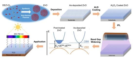
Band Gap Tuning of Films of Undoped ZnO Nanocrystals by Removal of Surface Groups


Abstract
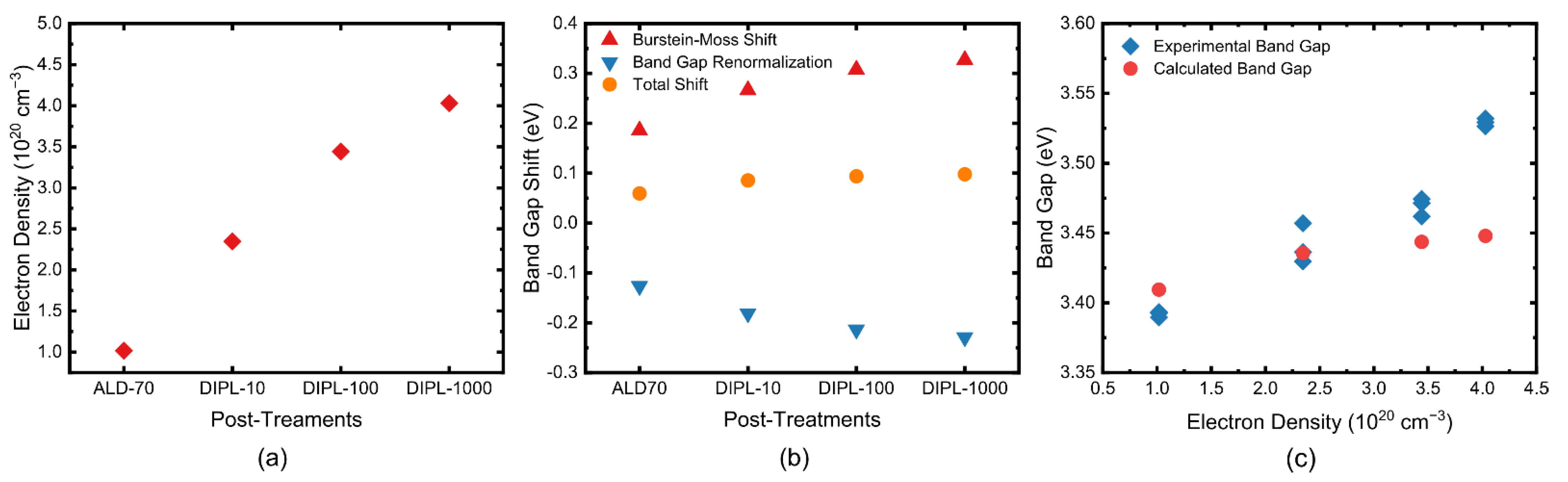
:
1. Introduction
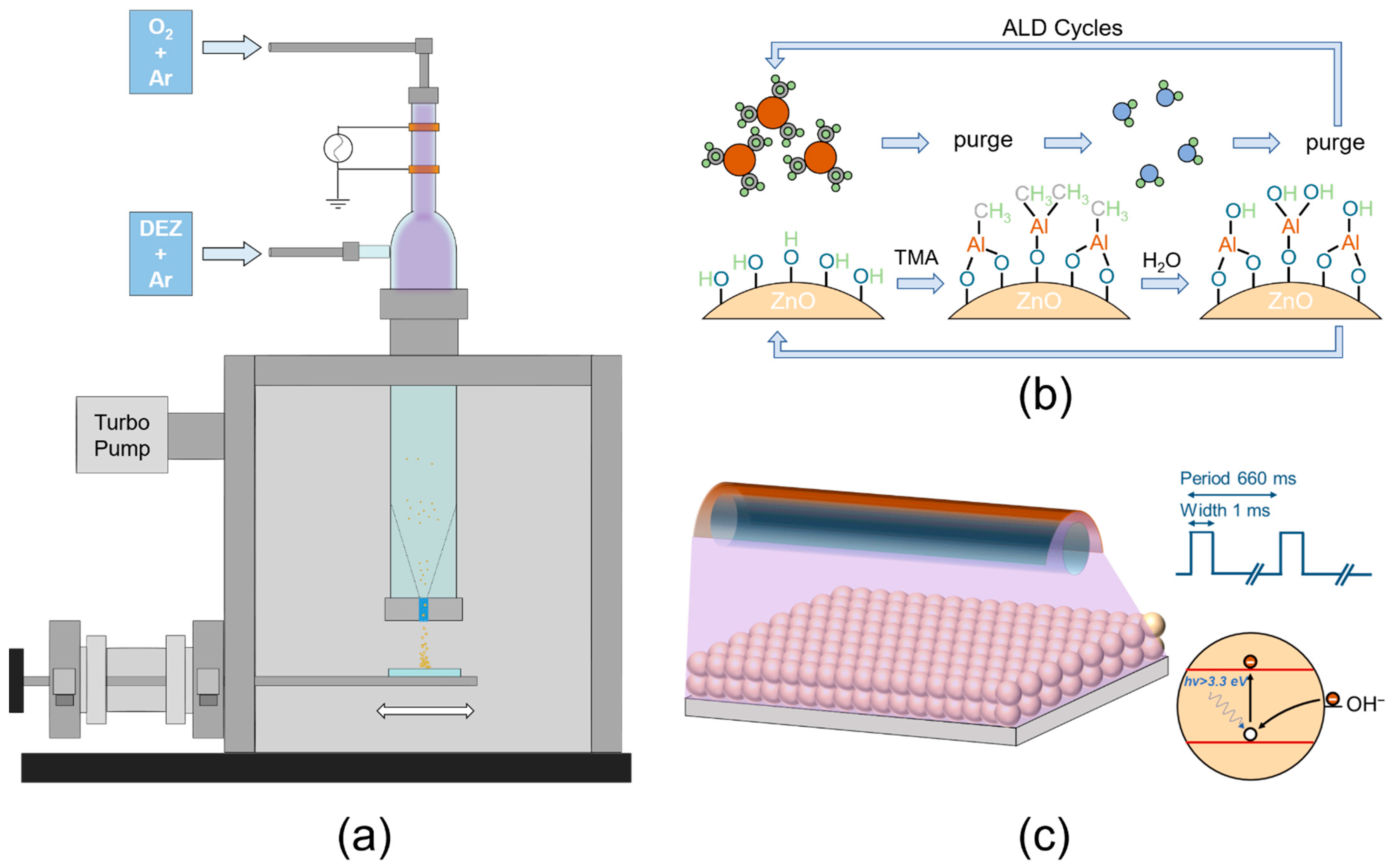
2. Materials and Methods
2.1. Sample Preparation and Post Treatments
2.2. Materials Characterization
3. Results
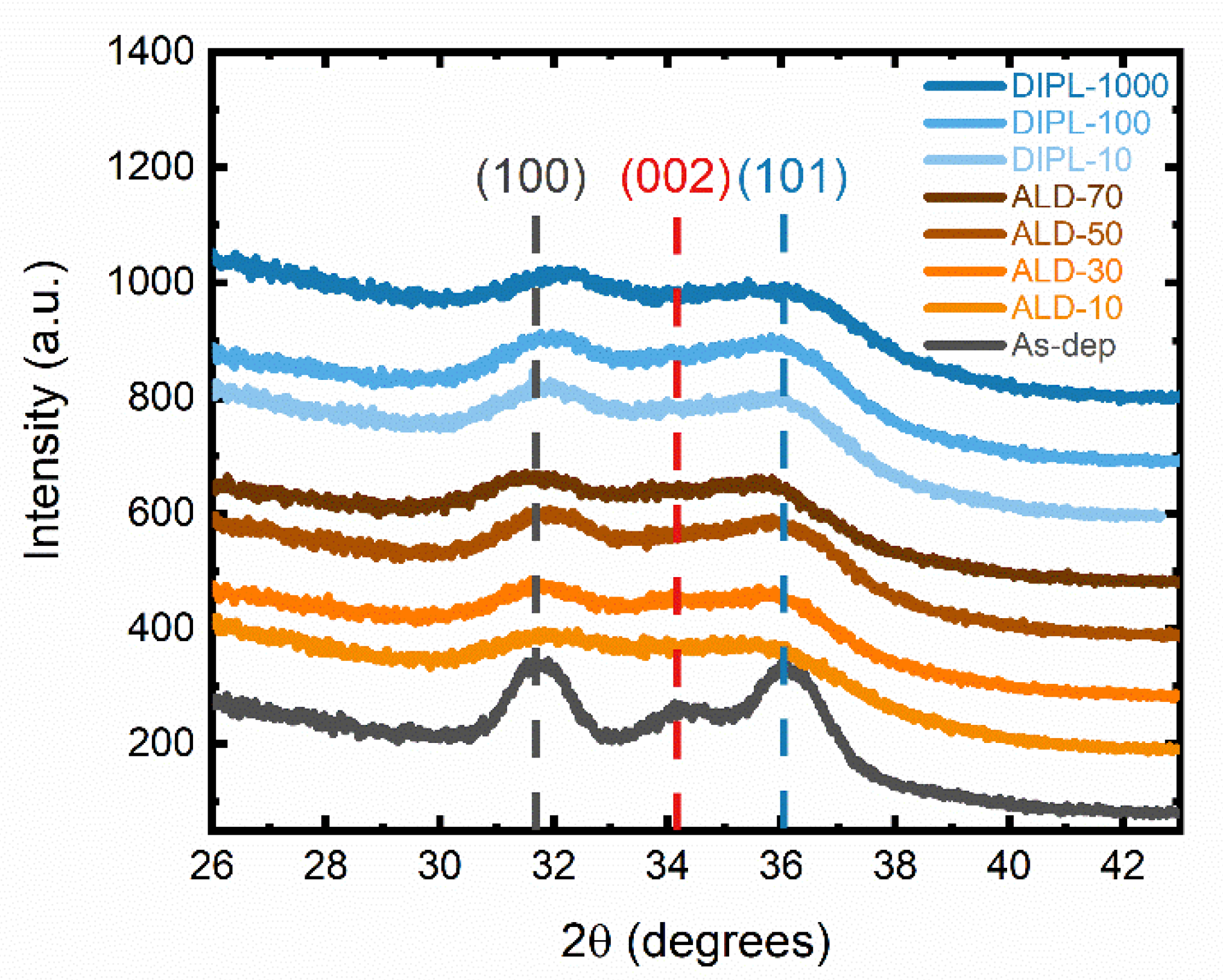
3.1. Characterization of ZnO NC Thin Films
3.2. Band Gap of ZnO NC Thin Films
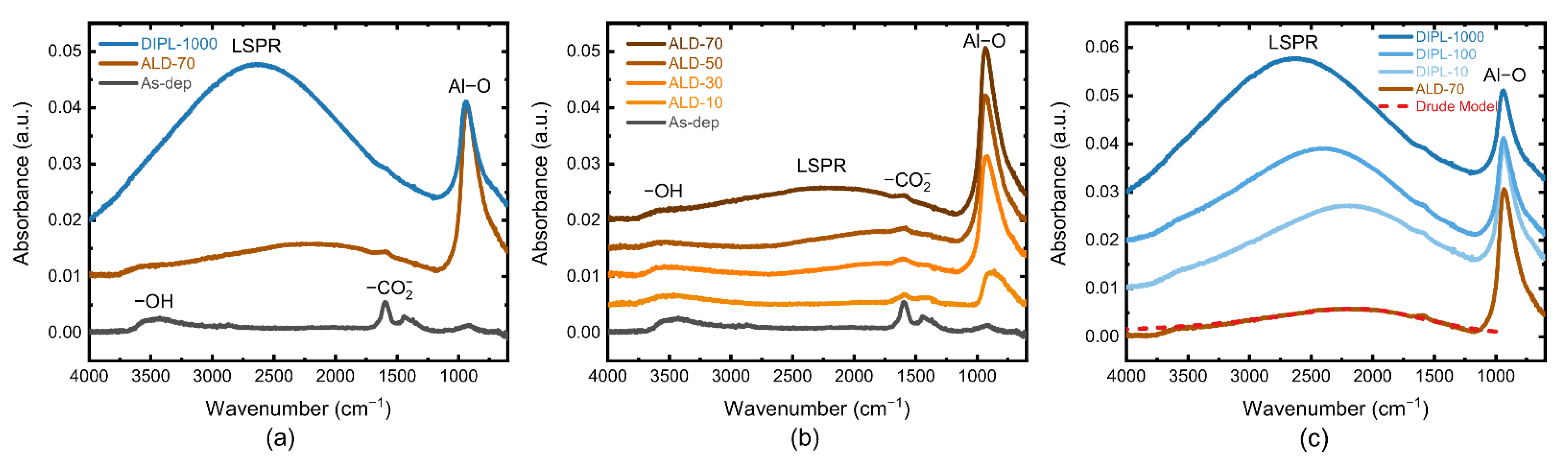
3.3. FTIR Study of ZnO NC Thin Films
3.4. Band Gap Tuning Mechanism
4. Discussion
5. Conclusions
Supplementary Materials
Author Contributions
Funding
Institutional Review Board Statement
Informed Consent Statement
Data Availability Statement
Conflicts of Interest
References
- Wang, Z.; Chen, C.; Wu, K.; Chong, H.; Ye, H. Transparent conductive oxides and their applications in near infrared Plasmonics. Phys. Status Solidi 2019, 216, 1700794. [Google Scholar] [CrossRef]
- Bo, R.; Zhang, F.; Bu, S.; Nasiri, N.; Di Bernardo, I.; Tran-Phu, T.; Shrestha, A.; Chen, H.; Taheri, M.; Qi, S. One-step synthesis of porous transparent conductive oxides by hierarchical self-assembly of aluminum-doped ZnO nanoparticles. ACS Appl. Mater. Interfaces 2020, 12, 9589–9599. [Google Scholar] [CrossRef]
- Buonsanti, R.; Llordes, A.; Aloni, S.; Helms, B.A.; Milliron, D.J. Tunable Infrared Absorption and Visible Transparency of Colloidal Aluminum-Doped Zinc Oxide Nanocrystals. Nano Lett. 2011, 11, 4706–4710. [Google Scholar] [CrossRef]
- Ozgur, Ü.; Hofstetter, D.; Morkoç, H. ZnO devices and applications: A review of current status and future prospects. Proc. IEEE 2010, 98, 1255–1268. [Google Scholar] [CrossRef]
- Minami, T. Present status of transparent conducting oxide thin-film development for Indium-Tin-Oxide (ITO) substitutes. Thin Solid Films 2008, 516, 5822–5828. [Google Scholar] [CrossRef]
- Illiberi, A.; Poodt, P.; Bolt, P.; Roozeboom, F. Recent Advances in Atmospheric Vapor-Phase Deposition of Transparent and Conductive Zinc Oxide. Chem. Vap. Depos. 2014, 20, 234–242. [Google Scholar] [CrossRef]
- Minami, T. Transparent conducting oxide semiconductors for transparent electrodes. Semicond. Sci. Technol. 2005, 20, S35–S44. [Google Scholar] [CrossRef]
- Kortshagen, U.R.; Sankaran, R.M.; Pereira, R.N.; Girshick, S.L.; Wu, J.J.; Aydil, E.S. Nonthermal plasma synthesis of nanocrystals: Fundamental principles, materials, and applications. Chem. Rev. 2016, 116, 11061–11127. [Google Scholar] [CrossRef]
- Kortshagen, U. Nonthermal plasma synthesis of semiconductor nanocrystals. J. Phys. D Appl. Phys. 2009, 42, 11061–11127. [Google Scholar] [CrossRef]
- Kortshagen, U.; Bhandarkar, U. Modeling of particulate coagulation in low pressure plasmas. Phys. Rev. E 1999, 60, 887. [Google Scholar] [CrossRef]
- Thimsen, E.; Johnson, M.; Zhang, X.; Wagner, A.J.; Mkhoyan, K.A.; Kortshagen, U.R.; Aydil, E.S. High electron mobility in thin films formed via supersonic impact deposition of nanocrystals synthesized in nonthermal plasmas. Nat. Commun. 2014, 5, 1–9. [Google Scholar] [CrossRef] [PubMed] [Green Version]
- Greenberg, B.L.; Robinson, Z.L.; Reich, K.V.; Gorynski, C.; Voigt, B.N.; Francis, L.F.; Shklovskii, B.I.; Aydil, E.S.; Kortshagen, U.R. ZnO Nanocrystal Networks Near the Insulator-Metal Transition: Tuning Contact Radius and Electron Density with Intense Pulsed Light. Nano Lett. 2017, 17, 4634–4642. [Google Scholar] [CrossRef] [Green Version]
- Agrawal, A.; Cho, S.H.; Zandi, O.; Ghosh, S.; Johns, R.W.; Milliron, D.J. Localized surface plasmon resonance in semiconductor nanocrystals. Chem. Rev. 2018, 118, 3121–3207. [Google Scholar] [CrossRef] [PubMed]
- Mariappan, R.; Ponnuswamy, V.; Suresh, P. Effect of doping concentration on the structural and optical properties of pure and tin doped zinc oxide thin films by nebulizer spray pyrolysis (NSP) technique. Superlattices Microstruct. 2012, 52, 500–513. [Google Scholar] [CrossRef]
- Banerjee, P.; Lee, W.-J.; Bae, K.-R.; Lee, S.B.; Rubloff, G.W. Structural, electrical, and optical properties of atomic layer deposition Al-doped ZnO films. J. Appl. Phys. 2010, 108, 43504. [Google Scholar] [CrossRef] [Green Version]
- Lu, J.G.; Ye, Z.Z.; Zeng, Y.J.; Zhu, L.P.; Wang, L.; Yuan, J.; Zhao, B.H.; Liang, Q.L. Structural, optical, and electrical properties of (Zn, Al) O films over a wide range of compositions. J. Appl. Phys. 2006, 100, 73714. [Google Scholar] [CrossRef]
- Sans, J.A.; Sánchez-Royo, J.F.; Segura, A.; Tobias, G.; Canadell, E. Chemical effects on the optical band-gap of heavily doped ZnO: MIII (M = Al, Ga, In): An investigation by means of photoelectron spectroscopy, optical measurements under pressure, and band structure calculations. Phys. Rev. B 2009, 79, 195105. [Google Scholar] [CrossRef]
- Holman, Z.C.; Kortshagen, U.R. A flexible method for depositing dense nanocrystal thin films: Impaction of germanium nanocrystals. Nanotechnology 2010, 21, 335302. [Google Scholar] [CrossRef] [PubMed]
- Borchert, H.; Shevchenko, E.V.; Robert, A.; Mekis, I.; Kornowski, A.; Grübel, G.; Weller, H. Determination of nanocrystal sizes: A comparison of TEM, SAXS, and XRD studies of highly monodisperse CoPt3 particles. Langmuir 2005, 21, 1931–1936. [Google Scholar] [CrossRef]
- Krautheim, G.; Hecht, T.; Jakschik, S.; Schröder, U.; Zahn, W. Mechanical stress in ALD-Al2O3 films. Appl. Surf. Sci. 2005, 252, 200–204. [Google Scholar] [CrossRef]
- Filatova, E.O.; Konashuk, A.S. Interpretation of the changing the band gap of Al2O3 depending on its crystalline form: Connection with different local symmetries. J. Phys. Chem. C 2015, 119, 20755–20761. [Google Scholar] [CrossRef]
- Makuła, P.; Pacia, M.; Macyk, W. How to correctly determine the band gap energy of modified semiconductor photocatalysts based on UV–Vis spectra. J. Phys. Chem. Lett. 2018, 9, 6814–6817. [Google Scholar] [CrossRef] [Green Version]
- Mang, A.; Reimann, K. Band gaps, crystal-field splitting, spin-orbit coupling, and exciton binding energies in ZnO under hydrostatic pressure. Solid State Commun. 1995, 94, 251–254. [Google Scholar] [CrossRef]
- Wang, X.; Jin, Y.; He, H.; Yang, F.; Yang, Y.; Ye, Z. Bandgap engineering and shape control of colloidal CdxZn1−xO nanocrystals. Nanoscale 2013, 5, 6464–6468. [Google Scholar] [CrossRef]
- Willets, K.A.; Van Duyne, R.P. Localized surface plasmon resonance spectroscopy and sensing. Annu. Rev. Phys. Chem. 2007, 58, 267–297. [Google Scholar] [CrossRef] [PubMed] [Green Version]
- Thomas, D.G. Interstitial zinc in zinc oxide. J. Phys. Chem. Solids 1957, 3, 229–237. [Google Scholar] [CrossRef]
- Elam, J.W.; George, S.M. Growth of ZnO/Al2O3 alloy films using atomic layer deposition techniques. Chem. Mater. 2003, 15, 1020–1028. [Google Scholar] [CrossRef]
- Ephraim, J.; Lanigan, D.; Staller, C.; Milliron, D.J.; Thimsen, E. Transparent conductive oxide nanocrystals coated with insulators by atomic layer deposition. Chem. Mater. 2016, 28, 5549–5553. [Google Scholar] [CrossRef]
- Burstein, E. Anomalous optical absorption limit in InSb. Phys. Rev. 1954, 93, 632. [Google Scholar] [CrossRef]
- Gibbs, Z.M.; LaLonde, A.; Snyder, G.J. Optical band gap and the Burstein–Moss effect in iodine doped PbTe using diffuse reflectance infrared Fourier transform spectroscopy. New J. Phys. 2013, 15, 75020. [Google Scholar] [CrossRef] [Green Version]
- Kreibig, U.; Vollmer, M. Optical Properties of Metal Clusters; Springer Science & Business Media: Berlin/Heidelberg, Germany, 2013; Volume 25, ISBN 3662091097. [Google Scholar]
- Bohren, C.F.; Huffman, D.R. Absorption and Scattering of Light by Small Particles; John Wiley & Sons: Hoboken, NJ, USA, 2008; ISBN 3527618163. [Google Scholar]
- Moss, T.S. The interpretation of the properties of indium antimonide. Proc. Phys. Soc. Sect. B 1954, 67, 775. [Google Scholar] [CrossRef]
- Lu, J.G.; Fujita, S.; Kawaharamura, T.; Nishinaka, H.; Kamada, Y.; Ohshima, T.; Ye, Z.Z.; Zeng, Y.J.; Zhang, Y.Z.; Zhu, L.P. Carrier concentration dependence of band gap shift in n-type ZnO: Al films. J. Appl. Phys. 2007, 101, 83705. [Google Scholar] [CrossRef]
- Pisarkiewicz, T.; Zakrzewska, K.; Leja, E. Scattering of charge carriers in transparent and conducting thin oxide films with a non-parabolic conduction band. Thin Solid Films 1989, 174, 217–223. [Google Scholar] [CrossRef]
- Ziabari, A.A.; Rozati, S.M. Carrier transport and bandgap shift in n-type degenerate ZnO thin films: The effect of band edge nonparabolicity. Phys. B Condens. Matter 2012, 407, 4512–4517. [Google Scholar] [CrossRef]
- Wolff, P. Theory of the band structure of very degenerate semiconductors. Phys. Rev. 1962, 126, 405. [Google Scholar] [CrossRef]
- Roth, A.P.; Webb, J.B.; Williams, D.F. Band-gap narrowing in heavily defect-doped ZnO. Phys. Rev. B 1982, 25, 7836. [Google Scholar] [CrossRef]
- Saw, K.G.; Aznan, N.M.; Yam, F.K.; Ng, S.S.; Pung, S.Y. New insights on the burstein-moss shift and band gap narrowing in indium-doped zinc oxide thin films. PLoS ONE 2015, 10, e0141180. [Google Scholar] [CrossRef] [Green Version]
- Auvergne, D.; Camassel, J.; Mathieu, H. Band-gap shrinkage of semiconductors. Phys. Rev. B 1975, 11, 2251. [Google Scholar] [CrossRef]
- Berggren, K.-F.; Sernelius, B.E. Band-gap narrowing in heavily doped many-valley semiconductors. Phys. Rev. B 1981, 24, 1971. [Google Scholar] [CrossRef]
- Jain, S.C.; McGregor, J.M.; Roulston, D.J. Band-gap narrowing in novel III-V semiconductors. J. Appl. Phys. 1990, 68, 3747–3749. [Google Scholar] [CrossRef]
- Lee, J.; Gao, W.; Li, Z.; Hodgson, M.; Metson, J.; Gong, H.; Pal, U. Sputtered deposited nanocrystalline ZnO films: A correlation between electrical, optical and microstructural properties. Appl. Phys. A Mater. Sci. Process. 2005, 80, 1641–1646. [Google Scholar] [CrossRef]
- He, H.P.; Zhuge, F.; Ye, Z.Z.; Zhu, L.P.; Wang, F.Z.; Zhao, B.H.; Huang, J.Y. Strain and its effect on optical properties of Al-N codoped ZnO films. J. Appl. Phys. 2006, 99, 23503. [Google Scholar] [CrossRef]
- Ylivaara, O.M.E.; Liu, X.; Kilpi, L.; Lyytinen, J.; Schneider, D.; Laitinen, M.; Julin, J.; Ali, S.; Sintonen, S.; Berdova, M. Aluminum oxide from trimethylaluminum and water by atomic layer deposition: The temperature dependence of residual stress, elastic modulus, hardness and adhesion. Thin Solid Films 2014, 552, 124–135. [Google Scholar] [CrossRef]
- Lu, H.; Tian, W.; Cao, F.; Ma, Y.; Gu, B.; Li, L. A self-powered and stable all-perovskite photodetector-solar cell nanosystem. Adv. Funct. Mater. 2016, 26, 1296–1302. [Google Scholar] [CrossRef]


Publisher’s Note: MDPI stays neutral with regard to jurisdictional claims in published maps and institutional affiliations. |
© 2022 by the authors. Licensee MDPI, Basel, Switzerland. This article is an open access article distributed under the terms and conditions of the Creative Commons Attribution (CC BY) license (https://creativecommons.org/licenses/by/4.0/).
Share and Cite
Zhang, C.; Tu, Q.; Francis, L.F.; Kortshagen, U.R. Band Gap Tuning of Films of Undoped ZnO Nanocrystals by Removal of Surface Groups. Nanomaterials 2022, 12, 565. https://doi.org/10.3390/nano12030565
Zhang C, Tu Q, Francis LF, Kortshagen UR. Band Gap Tuning of Films of Undoped ZnO Nanocrystals by Removal of Surface Groups. Nanomaterials. 2022; 12(3):565. https://doi.org/10.3390/nano12030565
Chicago/Turabian StyleZhang, Chengjian, Qiaomiao Tu, Lorraine F. Francis, and Uwe R. Kortshagen. 2022. "Band Gap Tuning of Films of Undoped ZnO Nanocrystals by Removal of Surface Groups" Nanomaterials 12, no. 3: 565. https://doi.org/10.3390/nano12030565
APA StyleZhang, C., Tu, Q., Francis, L. F., & Kortshagen, U. R. (2022). Band Gap Tuning of Films of Undoped ZnO Nanocrystals by Removal of Surface Groups. Nanomaterials, 12(3), 565. https://doi.org/10.3390/nano12030565