3.1. Er-Doped Tellurite Modified Silica (EDTS) on SiO2-on-Silicon Substrate
Figure 1a displays a backscattered (BSE) cross-sectional SEM image of bare SOS substrate, while
Figure 1b–d show BSE cross-sectional SEM images for samples fabricated when substrates were heated at temperatures of 400 °C (B400), 570 °C (B570), and 700 °C (B700). The thickness of the original silica layer (
Table 1) remained at ~1 μm, proving that no doping process actually occurred for sample B400, and the layer obtained was only typical deposited film. This finding indicated that a temperature of 400 °C is insufficient for the incoming plasma plume to modify the strong covalent bonds of silica. The film formed on the SOS was only Er-TZN glass film, with compositions presented in
Table 2, where the Te concentration was much higher than the Si concentration. The surface for the B400 sample appeared to be very rough with clusters of microparticles. Such film is unsuitable for EDWA because it could cause significant surface scattering and ultimately propagation loss for laser signals.
Figure 1c,d represent a cross section of samples produced at higher temperatures demonstrating the formation of Er-doped tellurite silica layer labelled as EDTS with thickness increasing with temperature. The elemental composition of the EDTS obtained from EDX-SEM and XPS for samples B570 and B700, as shown in
Table 2, proved that the EDTS consisted of combinations of elements from the target material and silica from the substrate surface. This finding indicated that cations, such as Te, Zn, Na, and Er, were removed from the target material and diffused into silica, thereby modifying the original silica network during the ULPD process. However,
Table 2 shows that the sample where the substrate was heated at 700 °C had a lower Te concentration than the sample prepared at 570 °C because of the volatility of Te that caused severe depletion through evaporation at a high temperature [
22,
23]. Nonetheless, the high temperature used to heat the substrate gave way to a relatively higher concentration of elements from the target glass, except Te, to dissolve into the silica.
As shown in
Table 1, the thickness and refractive index of sample B400 could not be accurately determined by the prism coupler because of its rough surface. Meanwhile, the higher temperature used caused the materials from Er–TZN to penetrate more into the silica, thus causing a thicker EDTS. The reduced concentration of Te in sample B700, which is a heavy element in the EDTS, caused the lower refractive index of this sample than B570. Therefore, the concentration of Te in the EDTS is an essential factor as it could control the refractive index, which, in turn, could contribute to the design of integrated optical waveguides by using the ULPD approach presented in this work.
Figure 2 shows the XRD patterns of SOS substrate and SOS doped with Er-TZN when the substrate was heated to 400 °C, 570 °C, and 700 °C. For samples B570 and B700, the EDTS obtained were amorphous, except the peak at 2θ = 69°, corresponding to underlying crystalline silicon, Si (100) from SOS substrate. Meanwhile, for B400, the deposited film was clearly crystalline with a distinct peak at 2θ = 19.16°, 28.86°, 49.02°, and 59.68°. The peaks at 19.16° and 59.68° refer to Zn
2Te
3O
8 based on the ICCD reference code: 04-012-2189 with each having miller indices of (111) and (332), whilst the peaks at 28.86° and 49.02° matched with Na
2TeO
3 with miller indices of (022) and (242), respectively (ICDD reference code: 00-035-1263).
The photoluminescence (PL) emission spectra of Er
3+-ions in the samples were measured using a 980 nm diode laser as the excitation source. The PL emission spectra of the layers produced at various temperatures are represented in
Figure 3. For sample B400, the spectrum shape obtained was clearly different from that of samples B570 and B700. The FWHM in sample B400 was broader (
Table 3) than in samples B570 and B700 and almost similar to that reported for tellurite glasses [
24,
25,
26]. For samples B570 and B700, the obtained FWHM was 20 nm and similar to the FWHM of other previously reported Er
3+-doped silicate glasses, such as phosphosilicate, soda-lime silicate, and borosilicate [
27,
28]. This also confirms, in addition to elemental analysis, that the Er-TZN had permeated into the silica glass network and transformed it into silicate glass. Sample B400 had a lower PL lifetime (5.26 ms) than samples B570 (12.29 ms) and B700 (11.12 ms). The obtained PL lifetime for the Er-doped tellurite glass layer was obviously much lower than erbium-doped silicate glass as reported for other erbium-doped tellurite glasses, which are TeO
2–GeO
2–Na
2O–ZnO–Er
2O
3 (5.7 ms) [
29], TeO
2–WO
3–Na
2O–Er
2O
3 (3.46 ms) [
30], and TeO
2–WO
3–Na
2O–Nb
2O
5–Er
2O
3 (3.7 ms) [
31]. The lower PL lifetime for sample B400 is due to it being essentially a tellurite host material with stoichiometry similar to the target glass. PL lifetime is well known to also depend strongly on host material [
32,
33]. In particular, it is closely related to the refractive index of the host material based on the Judd–Ofelt theory. According to the theory, lifetime has an inverse relationship with refractive index [
34,
35,
36]. Given that tellurite glass has a higher refractive index than silicate glass, it exhibited a lower lifetime, and this is the main reason that the PL lifetime for sample B400 was far lower than that for samples B570 and B700.
Figure 4 shows the XPS survey scan for samples fabricated using different substrate temperatures. For sample B400, the Te peak was obviously the highest among the samples, proving that tellurite is the predominant host material in the deposited layer. The absence of Si in sample B400 also confirms that there was no reaction in underlying SiO2 layer. For samples B570 and B700, the Er concentration was too low, and it could not be detected in the spectra survey. Er peaks that are often identified from Er 4d overlap with Si 2s peaks, which are more pronounced because of much higher silicon concentrations than the Er in samples B570 and B700. Furthermore, no peaks other than carbon (C 1s) and species from Er-TZN and silica were detected in the spectrum survey obtained. This finding indicated that no contaminants were present in the upper layer. For sample B700, the Te 3d
5/2, and Te 3d
3/2, peaks were very low compared with those in B570, and Te 2p
1/2 and Te 2p
3/2 peaks were absent, which validated the argument on the reduction of Te content in EDTS at higher temperatures.
Table 2 tabulates the element concentration for the surface layer of samples B400, B570, and B700, as calculated using a high-resolution scan of O 1s, Si 2p, Na 1s, Zn 2p
3/2, Te 3d
5/2, and Er 4p
3/2. Even though the value for the element concentrations derived from XPS was slightly different from EDX-SEM, the trend was still quite similar.
Figure 5 shows a high-resolution scan of Te 3d
5/2 for a sample fabricated with varying substrate temperatures. As expected, the high-resolution scan of Te 3d
5/2 for B400 was slightly different from that of the EDTS. No Te metal could be detected for this deposited layer, indicating that the amount of oxygen is sufficient in the layer. Surprisingly, TeO
3 was dominant in this network. The peak located at ~574 eV is typically attributed to tellurium suboxide [
37,
38]. For the B700 sample, the low density of the tellurium species in EDTS made the scan results have much noise and made deconvolution processes difficult, possibly causing it to be less accurate.
Figure 6 shows the Raman spectra for samples prepared at different substrate temperatures. Samples B570 and B700 reported a wavenumber peak of 521 cm
−1 attributed to single-crystalline silicon derived from the substrate [
39,
40]. This peak appeared to be lower for sample B700 because the EDTS for this sample was thicker than that for B570, which, in turn, caused the signal from the Si substrate to be weak. By contrast, the Si peak was invisible in sample B400 because of the thick layer of deposited Er-TZN and the SiO
2 layer on a silicon substrate. Deconvolution of the spectrum was carried out for sample B570 to extract information about the hidden peaks for the EDTS layer.
The Raman spectra for sample B570 were deconvoluted into nine Gaussian bands (A–I), and the results are shown in
Figure 7. The peak at energies lower than 250 cm
−1 is named band A and considered a boson peak [
41,
42]. The Raman peak observed near band B (272 cm
−1) is associated with a bending vibration of the TeO
3 trigonal pyramid (tp) [
43,
44,
45]. The appearance of TeO
3 was also detected by XPS, as shown in
Figure 5. Band C, which was in the range of 430–500 cm
−1, is commonly associated with the Si-O-Si bending of Q
4 species [
39,
46,
47]. The peak around band E (590–650 cm
−1) is attributed to the Si-O-Si bridges (bending vibration) between two Q
2 species [
46,
48]. The emergence of a peak in the region of bands F (770–790 cm
−1) and G (900–1000 cm
−1) is often assigned as antisymmetric Si vibration in tetrahedral oxygen cage (Q
4) [
39,
46,
49] and Si-O-Si stretching of Q
2 components, respectively [
46,
50]. The bands at a higher frequency located at bands H (~1160 cm
−1) and I (~1544 cm
−1) are associated with Er-related fluorescence, whilst the prominent peak at band D (521 cm
−1) is referred to as silicon from the substrate. Meanwhile, the peak around ~250–280 cm
−1 associated with TeO
3 seemed more pronounced for sample B570 than for sample B700 (
Figure 6) because of the higher Te density in B570.
3.2. Doped Layer on Si3N4-on-Silicon Substrate
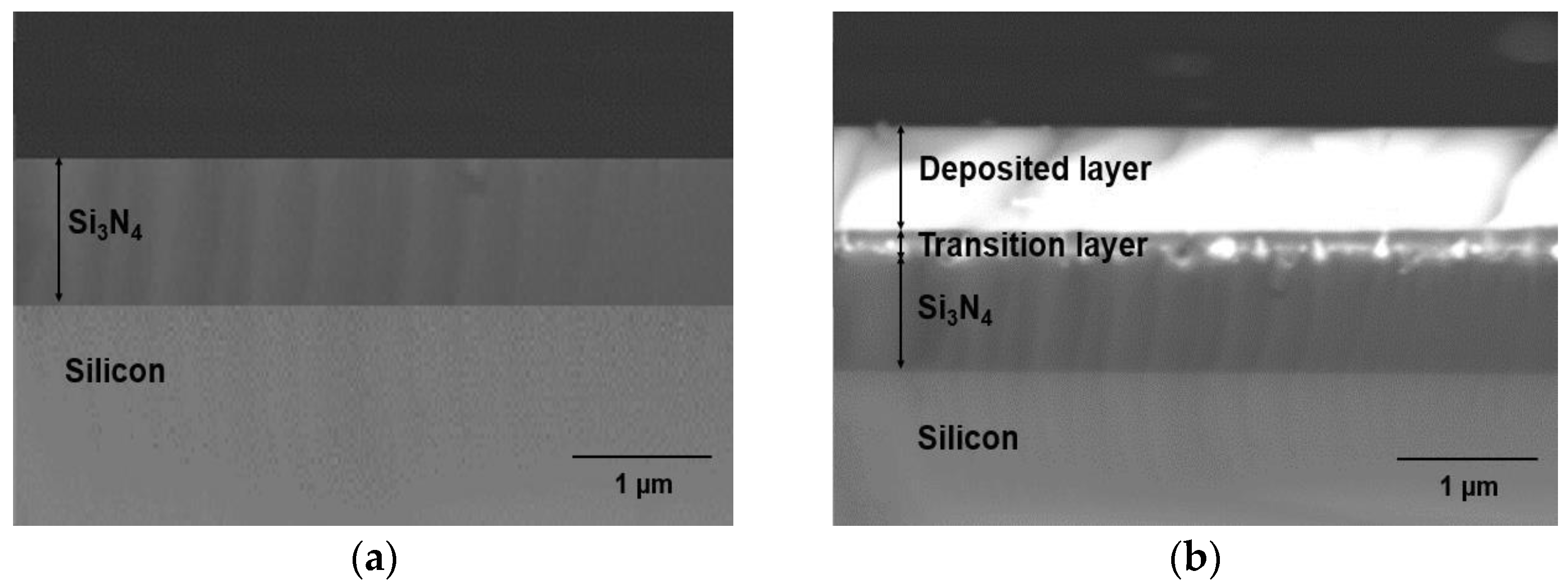
Figure 8a shows a BSE cross-sectional SEM image of a Si
3N
4-on-silicon substrate prior to ULPD trials, whilst SEM images for samples K470, K520, K570, K600, and K650 are shown in
Figure 8b–f. As
Figure 8b illustrates, deposition of Er-TZN onto the substrate occurred. The layer formed on the Si
3N
4 substrate appeared uniform and smooth. However, only a small amount of Er-TZN successfully penetrated Si
3N
4, indicating that a temperature of 470 °C is not sufficiently high to break the Si-N bond. Only a few of the energetic elements of Er-TZN managed to enter into the Si
3N
4 molecular network, as could be seen around the materials interface. According to the SEM images in
Figure 8c–f, for samples fabricated with a higher temperature of 520–650 °C, Er-TZN successfully diffused into the Si
3N
4. However, all the images of the doped layer demonstrated that the doping was not as uniform as doping silica with Er-TZN. Although elements from the target material managed to penetrate Si
3N
4, they were discretely distributed, as depicted by the grayscale variations in the doped layers. This largely inhomogeneous layer appeared to be partly porous, and, in certain areas, an accumulation of specific elements was observed. The SEM images of the surface of the doped layer also showed that it was very uneven and rough, as shown in
Figure 9.
The thicknesses of the upper layers for all of the samples are summarised in
Table 4. For sample K470, the thickness of the Si
3N
4 underneath the upper layer was less than the original thickness of 1 μm, which indicated that doping occurred, even though only a small amount was found on the Si
3N
4 surface. For samples K520, K570, K600, and K650, the upper layer thicknesses could not be precisely determined, and they showed large errors due to their very rough surfaces. However, the estimated thickness obtained showed a linear relationship between thickness and the temperature used to heat the substrate. Additionally, the thickness of the Si
3N
4 underneath the doped layer became smaller with an increase in substrate temperature. This finding indicated that the material target could react with Si
3N
4 more thoroughly at higher temperatures. The refractive index and thickness, which were supposedly measured using a prism coupler, could not be measured because of the uneven surface of the doped layer.
Figure 10 shows two different positions in sample K470 measured by EDX-SEM to obtain the elemental concentrations at these particular positions, and the results are shown in
Table 5. As the upper layer of sample K470 was only a deposited layer, it was expected to have the properties of tellurite-based glass used as a target material. The high concentration of Te at position 1 confirmed this expectation. For position 2, which is located near the interface of the deposited region and Si
3N
4 but within the Si
3N
4, some elements from the target material were mostly oxygen. The smaller atomic size of oxygen than that of Te, Zn, Na, and Er enabled a few energetic ions/atoms of oxygen to successfully penetrate the Si
3N
4 and oxidise some of it. However, the lower temperatures evidently hindered deeper modification of the Si
3N
4 layer further. The area scan performed for the sample to determine the distribution of elements in sample K470 is shown in
Figure 11. The negligible presence of elements Si and N in the upper layer confirmed that the upper layer consisted of elements from Er-TZN. Besides, the area scan obtained showed an intermediate region between the deposited layer and Si
3N
4 composed of Si, O, Te, Zn, Na, Er, and N. However, the area scan for Er was less obvious because of its deficient concentration, resulting in considerable noise in the scan results.
An area scan was performed to view the entire elemental distribution present in K600 (
Figure 12). The elements were clearly distributed unevenly. Surprisingly, the concentration of N in the doped layer was very low compared with its concentration in Si
3N
4, which was supposedly around ~57.1 %. Nitrogen was considered lost in the form of nitrogen gas when the tellurite glass reacted with Si
3N
4, and this phenomenon was also reported by Watanabe et al. [
51]. Failure to obtain a very uniform doped layer, such as in the case of EDTS, was probably due to the substrate temperature not being sufficiently high. The melting temperature of Si
3N
4 (1900 °C) was higher than that of silica (1710 °C). Therefore, higher temperatures may be required to allow the dissolution of Er-TZN into Si
3N
4 with homogeneous layer formation. Additionally, the failure to obtain homogeneously doped layers may be due to the SiO
2 amorphous network, which is somewhat different from Si
3N
4. Unlike the local structure of silica, which contains adjustable and flexible Si-O-Si- bridging bonds, Si
3N
4, consists of Si-N-Si bonds that are rendered rigid as N requires bonding with three Si rather than two to form a stable configuration. As a consequence, its network structure is much more constrained than that of silica [
52], making it difficult for the elements from Er-TZN to diffuse into Si
3N
4 and modify it. This leads to the formation of pores and cavities and the accumulation of certain elements for Si
3N
4 samples. A higher temperature could be expected to help loosen the strong Si-N bonds. Nonetheless, the more rigid Si
3N
4 structure caused it to have higher internal stress levels and thus to crack more easily. This problem was not observed for samples fabricated using an SOS substrate.
Figure 13a,b show the surface images of samples that used different substrates (SiO
2 and Si
3N
4) with the same process parameters and target material. The images were taken under an optical microscope near the edge of the doped layer. The findings clearly showed that the undoped Si
3N
4 layer on silicon cracked after the sample fabrication process.
Figure 14 shows the XRD patterns of the Si
3N
4-on-silicon substrate and samples K470, K520, K570, K600, and K650. The patterns showed that all samples were in a mixed amorphous–crystalline phase. The indexed peaks assigned to the possible crystalline structures are also shown in
Figure 14. The 2θ peak located at approximately ~69° is a crystalline Si (100) peak originating from the silicon substrate. For sample K470, eleven peaks were detected, namely, 23.38°, 27.87°, 38.63°, 40.61°, 43.61°, 46.42°, 48.73°,49.95°, 57.24°, 63.11°, and 65.98°, which correspond to Te (ICCD reference code: 00-036-1452). The appearance of Te crystallite peaks is attributable to the transition layer between the deposited and Si
3N
4 layers. For the doped layer of samples K520–K650, the intensity and number of crystalline peaks increased when higher substrate temperatures were used because crystallisation occurs more easily at high temperatures [
53,
54]. The crystalline peaks for SiO
2 (ICCD reference code: 00-039-1425) and Na
2Zn
3 (SiO
4)
2 (ICCD reference code: 00-012-3700) started to appear when the sample was heated at 600 °C, and they became more pronounced at higher temperatures. In addition, for the doped layer, the crystalline phase of Te increased in number and intensity with respect to increasing temperature.
Figure 15 presents the Raman spectra for the Si
3N
4-on-silicon substrate and samples fabricated with various substrate temperatures. The Raman spectra for sample K470 (
Figure 15b), comprising tellurite-based glass, were different compared with samples prepared at higher temperatures. As shown in
Figure 15c–f, all Raman spectra showed metallic tellurium peaks (122 and 141 cm
−1). This finding indicated that the tellurium cluster was likely to form within this doped layer and coincides with the findings from XRD. However, these two peaks were less pronounced in sample K470, suggesting that most of the Te in this sample was present in oxide form rather than metallic form. The stoichiometry of Er-TZN was better preserved in the deposited film than in the doped layer. The Raman spectrum for K470 was similar to that for B400 (
Figure 6a) because both of them were deposited tellurite-based layers. The decrease in Si peak intensity from samples K520 to K650 indicated that the thicknesses of the doped layer increased for samples fabricated at higher substrate temperatures. The Raman spectra for samples K520, K570, K600, and K650 (
Figure 15c–f) were similar to the EDTS, and only the appearance of peaks at 122 and 141 cm
−1 distinguished them. Therefore, the assignment of all other peaks in the spectra was the same as discussed for the EDTS, as the contribution of N was not detectable.
Figure 16 displays the XPS survey spectrum for sample K570. The spectrum pattern obtained resembled that of the EDTS. The absence of N confirmed that N is released when Er-TZN reacts with Si
3N
4. The distinct peak of N 1s that was expected at a binding energy of around 398 eV was not observed in the obtained spectra. Therefore, N is present only in very small quantities or virtually absent in the doped layer. The presence of Si in the spectral survey verified once again that Er-TZN successfully entered into the Si
3N
4 layer and formed a predominantly silicate-based layer.
The PL emission spectra for the samples are shown in
Figure 17. For K470, the FWHM of the spectra was broader than that of the others, also indicating that the upper layer was a tellurite-based material. The low PL lifetime (4.97 ms) and an FWHM value of approximately 33 nm (
Table 6) obtained were comparable with those reported for tellurite glass [
24,
55]. As shown in
Table 6, samples K520, K570, K600, and K650 had a PL lifetime of between 9 and 10 ms and FWHMs of 20 nm. This finding indicated that the doped layer was silicate based, as with the EDTS. If the doped layer is Si
3N
4 based, it could show a lower lifetime in the range of 0.2–7 ms with an FWHM broader than that of a typical Er-doped silicate-based material [
56,
57,
58]. As shown in
Table 6, the higher PL intensity and the lower lifetime of samples prepared at higher substrate temperatures signified that the Er density is higher in the doped layer when the substrate is heated to a higher temperature.


