Abstract
Low-frequency electronic noise is an important parameter used for the electronic and sensing applications of transistors. Here, we performed a systematic study on the low-frequency noise mechanism for both p-channel and n-channel MoTe2 field-effect transistors (FET) at different temperatures, finding that low-frequency noise for both p-type and n-type conduction in MoTe2 devices come from the variable range hopping (VRH) transport process where carrier number fluctuations (CNF) occur. This process results in the broad distribution of the waiting time of the carriers between successive hops, causing the noise to increase as the temperature decreases. Moreover, we found the noise magnitude for p-type MoTe2 FET hardly changed after exposure to the ambient conditions, whereas for n-FET, the magnitude increased by nearly one order. These noise characteristics may provide useful guidelines for developing high-performance electronics based on the emerging transition metal dichalcogenides.
1. Introduction
With the scaling of Si-based transistors approaching its limit, two-dimensional materials, as the possible building blocks of next generation electronics and optoelectronics, have attracted world-wide interest [1,2,3,4]. Although the zero-band gap of graphene greatly constrains its use in logic circuits, other 2D materials or derivatives, such as black phosphorus and transition-metal dichalcogenides (TMDs), show superior electrical and optoelectrical performance, and are considered to be promising candidates for the development of post-silicon devices [4,5,6,7,8,9,10,11,12]. 2H-type molybdenum ditelluride (MoTe2) is a layered compound with a band gap ranging from 0.81 eV (indirect) for bulk to 1.13 eV (direct) for monolayer, enabling its excellent performance in tunneling transistors, with high tunneling current and optoelectronic devices operating from the visible to the near-infrared range [11,13,14,15,16]. Moreover, due to its ambipolar transport property and its ability to improve mobility by tuning its carrier conduction type rationally, a variety of functional electronic devices can be realized, such as complementary metal-oxide-semiconductor transistors, logic inverters, and PN junctions, which paves the way for developing MoTe2-based high-performance electronics and optoelectronics [11,17,18,19,20].
Low-frequency noise usually manifests itself as slow fluctuations in the drain–source current, resulting from channel conductivity fluctuations [21,22,23,24]. It is a basic performance-limiting factor of electronic devices or circuits, in that the sensitivity and accuracy of electronic devices, such as sensors, amplifiers, or other digital and analog electronic devices, are ultimately defined by it [25,26,27,28]. With the decrease in circuit characteristic size, low-frequency noise becomes very important to the performance of the circuit [25,29,30,31,32,33,34,35]. Previous reports on low-frequency noise in graphene and MoS2 field-effect transistors suggest that the origin and mechanism of low-frequency noise is strongly dependent on the properties of the channel materials and device fabrication process [25,26,27,28,33,36,37,38]. To develop high-performance MoTe2-based electronic devices, a thorough characterization of specific features of low-frequency noise and the methods to reduce it is required.
In this work, we investigate the low-frequency noise in MoTe2 ambipolar field-effect transistors (FET). Noise measurement reveals that the noise mechanisms for both p-type and n-type conduction originate in CNF, causing the noise to increase as the temperature decreases. Subsequently, we find that large contact resistance at the metal–MoTe2 interface dominates the electrical and noise characteristics of the transistors in the “on” state. Finally, we investigate the impact of ambient conditions on the noise performance of MoTe2 n-FET and p-FET, finding that the noise in n-FET and p-FET changes variably following exposure to the atmospheric environment. The noise magnitude of n-FET increases by nearly one order, while in p-FET, little change is shown.
2. Materials and Methods
MoTe2 thin flakes were mechanically exfoliated using the Scotch tape method and transferred onto a degenerately n-doped Si/SiO2 (300 nm) substrate. The target MoTe2 thin flakes were identified by measuring the Raman scattering spectra with a 633 nm laser under an optical microscope, and the thickness of the flakes were determined by atomic force microscopy combined with the optical contrast. Standard electron-beam lithography was employed to define the electrical contact, and a metal stack of Cr/Au (5/60 nm) was deposited by electron beam evaporation. The electrical characterization of MoTe2 FET was performed in a lakeshore probe station (pressure lower than 10−5 Torr) using a Keithley 4200-SCS (Tektronix Inc., Beaverton, OR, USA) and a custom PDA fast probe noise measurement system.
3. Results
3.1. Basic Characteristics
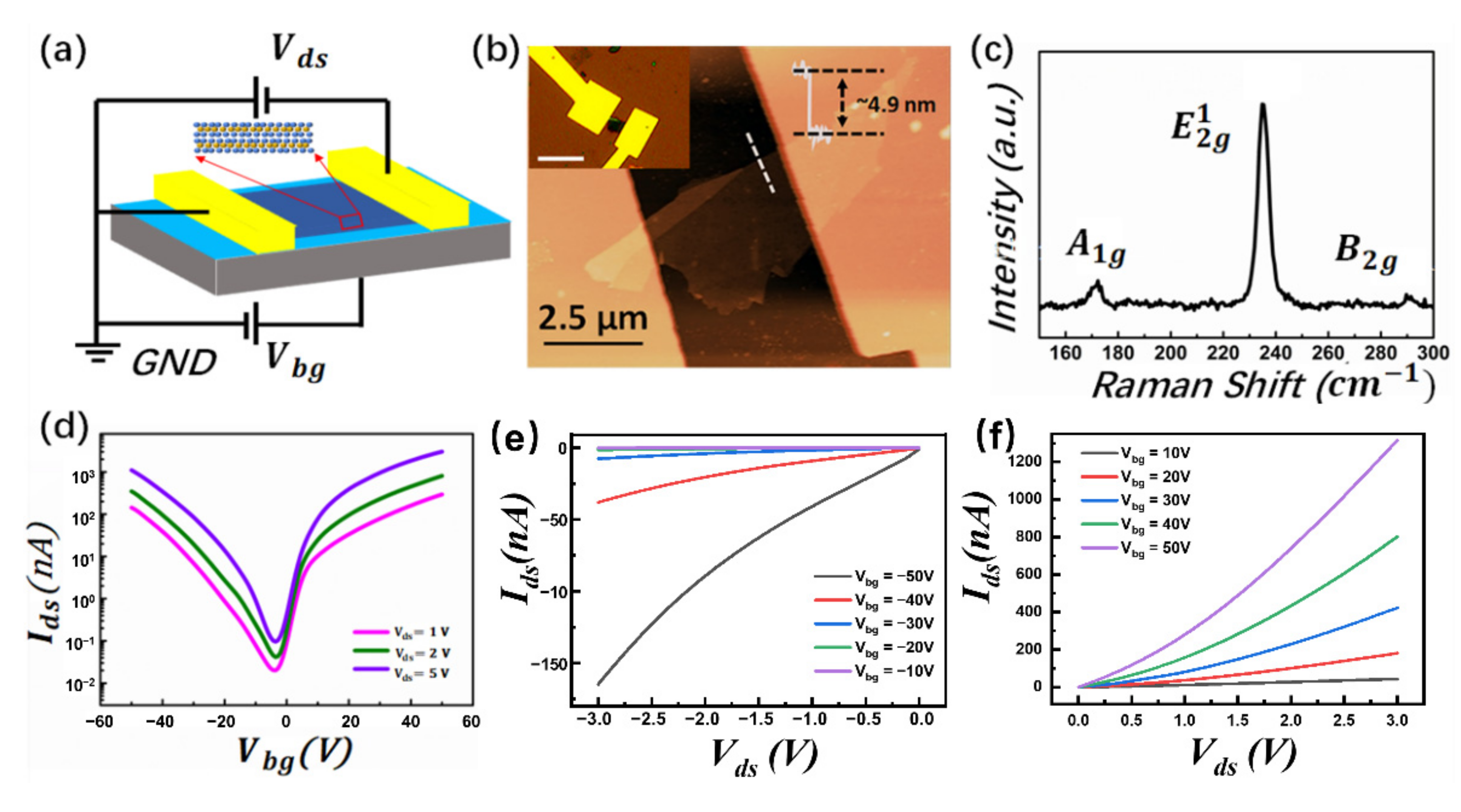
A schematic image of the MoTe2 field-effect transistor is shown in Figure 1a. The thickness of the flake was confirmed to be 4.9 nm by a surface line profile, as shown in Figure 1b, and the inset is an optical image of the device. Figure 1c is the Raman spectrum collected from the position indicated in Figure 1b. The peaks at around 171, 234, and 289 cm−1 can be attributed to the A1g, E12g, and B12g vibration modes, respectively, which is consistent with previous reports [13,14,15]. The room-temperature transfer characteristics of the device under different bias voltages are shown in Figure 1d. The increase in the drain current Ids with increasing gate voltage for both negative and positive polarities demonstrates the ambipolar operation of the MoTe2 FET, and the obvious saturation trend of the drain current at positive gate voltage (~7.5 V) can be a result of the contact resistance at the metal–MoTe2 interface [39]. The on/off ratio at Vds = 1.0 V is found to be ~7.1 × 10³ for MoTe2 p-FET, and ~1.5 × 10⁴ for MoTe2 n-FET, respectively. Field-effect mobility can be extracted from the equation:

Figure 1.
(a) Schematic image of MoTe2 transistor. (b) Atomic force microscope image of the transistor. The inset is the optical image of the transistor, scale bar is 5μm. (c) Raman spectrum of the MoTe2 measured under 633 nm laser flake in (b). (d) Transfer curves of the MoTe2 transistor with the back gate voltage sweeping from −50 to 50 V at a step of 0.8 V at different bias voltage: Vds = 1.0 V, 2.0 V, and 5.0 V, respectively. (e) Output curves of the transistor with bias voltage swept from −3.0 V to 0 V under different back gate voltages ranging from −50 to −10 V at a step of 10 V. (f) Output curves of the transistor with bias voltage swept from 0 to 3 V under different back gate voltages ranging from 10 to 50 V at a step of 10 V.
In this equation, L and W are the length and width of the channel, respectively. Cox is the gate oxide capacitance per unit area, and Vds is the source–drain bias voltage. The linear fitting was taken at the linear region of the transfer characteristics, and a mobility of 2.66 cm2/Vs for hole and 2.03 cm2/Vs for electron can be extracted, respectively. Figure 1e,f reveal the output characteristics of the MoTe2 FET with a bias voltage ranging from −3 to 0 V for p-FET, and 0–3 V for n-FET at different gate voltages. The good linear shape at small bias voltage and the obvious saturation of the current for p-FET imply that the contact between MoTe2 and metal electrode is ohmic or the contact resistance is comparably small. However, for n-FET, the drain current increases nonlinearly with bias voltage, indicating the existence of significant contact resistance at the metal–MoTe2 interface, which will suppress the electron injection from the metal electrode into the conducting channel and may cause series resistance noise [40].
3.2. Noise Characteristics
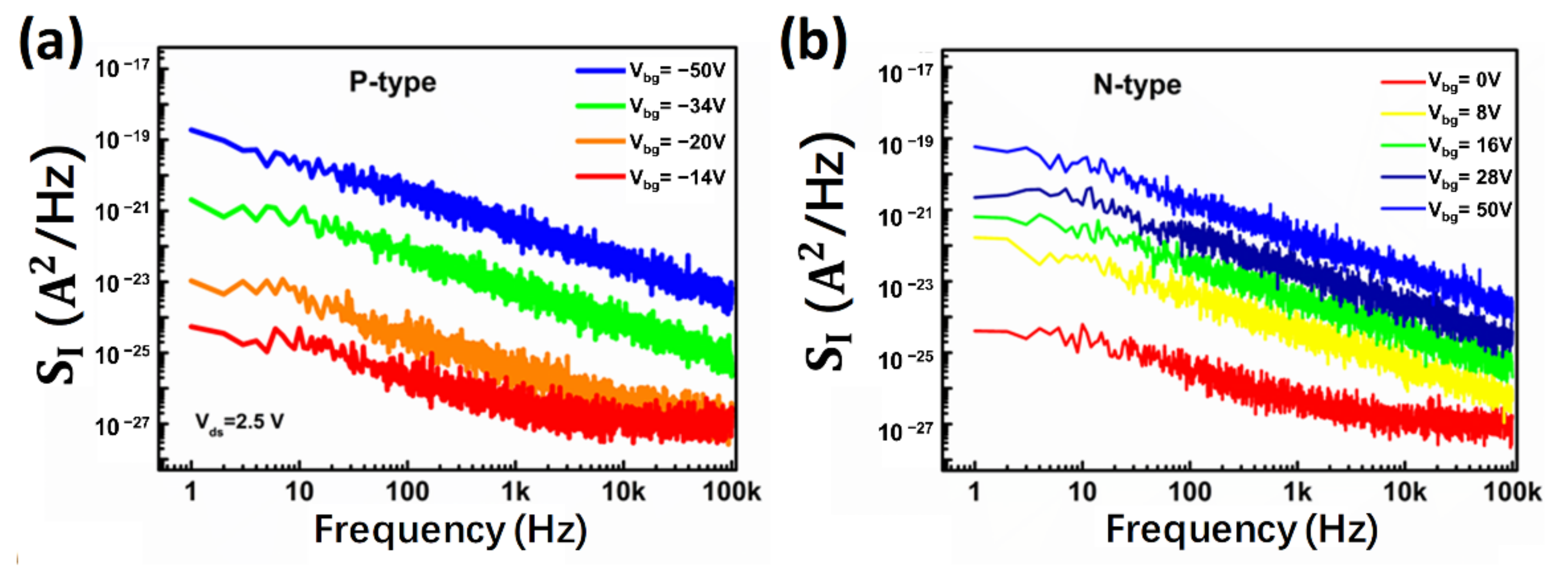
The noise characterization of MoTe2 FET is shown in Figure 2. The noise power spectral density SI of the MoTe2 p-FET at four different gate voltages between 1 Hz to 100 kHz with a bias voltage kept at Vds = 2.5 V is shown in Figure 2a. When the p-FET is in the “on” state, the noise spectra follow the typical 1/f dependence and can be quantitatively characterized by

Figure 2.
(a) Noise power spectral density SI as a function of frequency at different gate voltages for MoTe2 p-FET. (b) Noise power spectral density SI as a function of frequency at different gate voltages for MoTe2 n-FET.
In this equation, SI is the current noise power spectral density, A is the noise amplitude, Ids is the current through the device channel, f is the frequency, and β is the frequency exponent. However, when the gate voltage is close to the flat band voltage, or the device is in the “off” state, the noise spectra at a high frequency increase and deviate from 1/f dependence because of the instrumental noise floor. Figure 2b shows the noise characteristics of the MoTe2 n-FET in the same device and similar behavior can be observed.
The extracted frequency exponent β as a function of Vbg was extracted from a least-square fit of Figure 2a using Equation (2), which ranges from 0.95 to 1.1 in the “on” state as shown in Figure 3a. To determine whether the metal–MoTe2 contact barrier contributes to the noise of the MoTe2 FET, the normalized noise power spectra of both p-FET (Vbg = −50 V) and n-FET (Vbg = 46 V), as a function of frequency at different bias voltages, were performed, as shown in Figure 3b. It was found that the normalized noise power spectra for p-FET are independent of the bias voltage, indicating that the noise mainly originated from the MoTe2 conducting channel itself. However, for n-FET, the normalized noise power spectra are strongly dependent on bias voltage, suggesting the contact barrier is one of the main contributors to the noise of n-FET. These results are consistent with initial DC characterization results that significant contact resistance exists at the metal–MoTe2 interface.
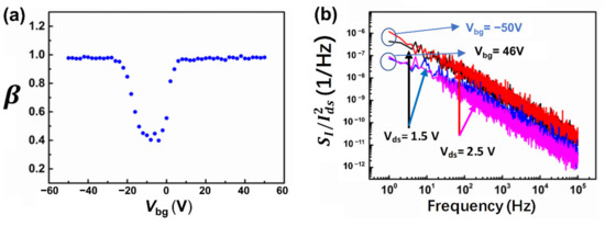
Figure 3.
(a) Frequency exponent β as a function of gate voltage. (b) Normalized noise spectra as a function of frequency at different bias voltage: Vds = 1.5 V, 2.5 V under different gate voltage: Vbg = −50 V, 46 V.
There are two models to describe the noise mechanism of the conventional FET: the carrier number fluctuation (CNF) model, which can be expressed by:
where Svfb is the flat-band voltage spectral density and q is the elementary charge, KB is the Boltzmann constant, T is the absolute temperature, Nit is the effective trap density, and Cox is the gate unit capacitance, respectively. The other model is the Hooge mobility fluctuation (HMF) model which is expressed by
where the Hooge parameter αH is an empirical dimensionless constant. If the series resistance contributes to the low-frequency noise, the total current noise changes into the form
where SRsd is the spectral density of series resistance [22,23]. From the equation, we can see that if the normalized drain current noise increases at a high current, it can be indicative of an enhanced low-frequency noise contribution of the series resistance.
To uncover the noise mechanism of this few-layer MoTe2-based transistor, at f = 100 Hz and its corresponding at 300 K as a function of the drain current for the MoTe2 p-FET and n-FET are plotted in Figure 4a,b, respectively. From Figure 4a, we can observe that and its corresponding follow the same trend over a wide drain current range, indicating that the low-frequency noise in MoTe2 p-FET comes from the carrier number fluctuation [24]. However, for n-FET, as shown in Figure 4b, we found that and its corresponding follow the same trend. At small currents larger than 2.0 × 10⁻⁷ A, the normalized noise power spectra deviate from their corresponding and start to increase alongside the drain current. Therefore, when the drain current is Ids < 2.0 × 10⁻⁷ A, noise is from the carrier number fluctuation, while when the drain current is Ids > 2.0 × 10⁻⁷ A, the noise of the n-FET mainly comes from the metal–MoTe2 contact barrier, which is consistent with results shown in Figure 3b.
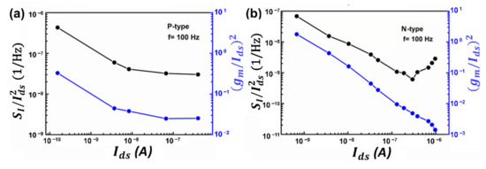
Figure 4.
(a) and its corresponding as a function of drain current for MoTe2 p-FET. (b) and its corresponding as a function of drain current for MoTe2 n-FET.
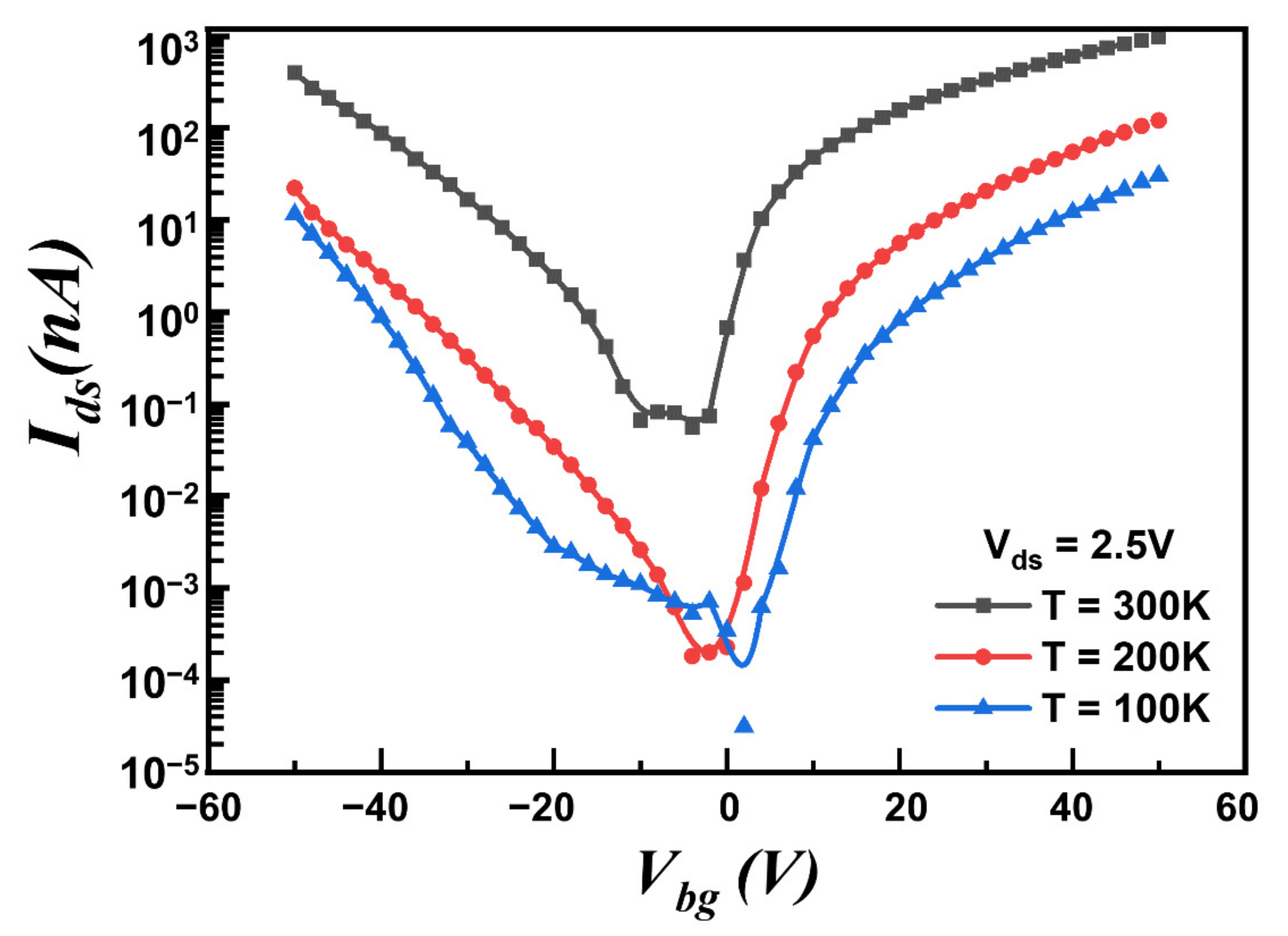
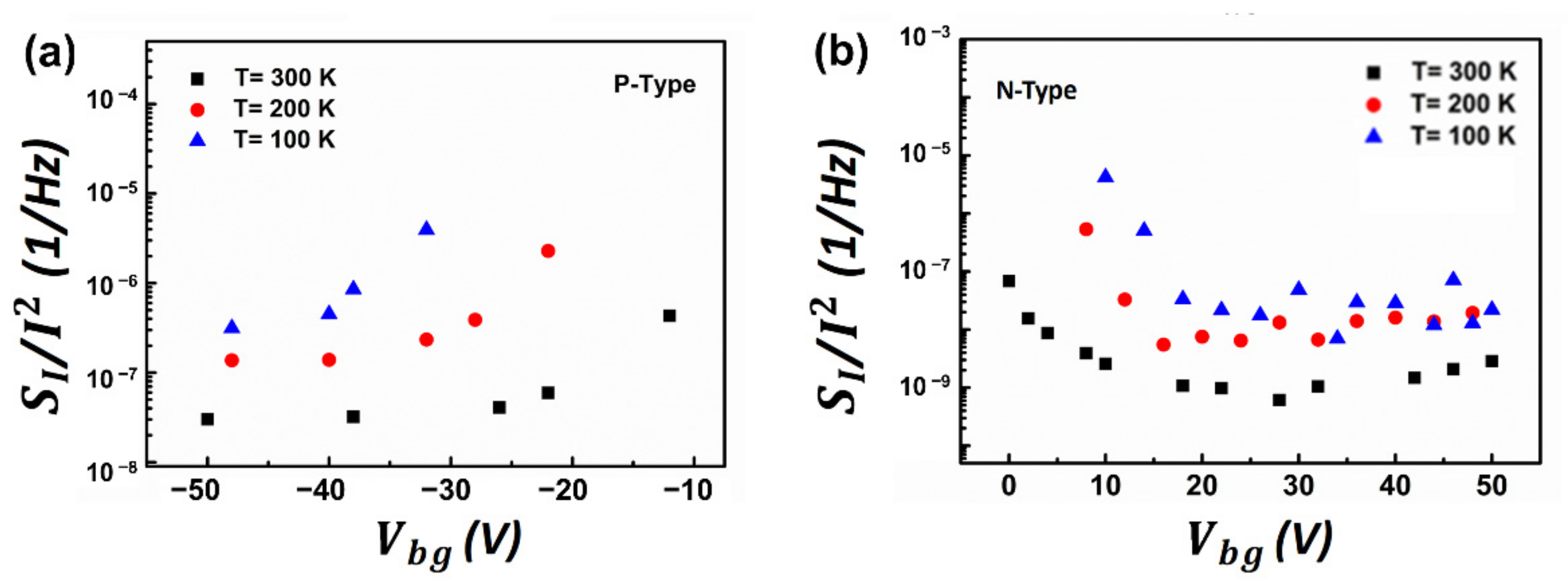
To further investigate the noise mechanisms, we characterized the transfer characteristics of the device (Figure 5), and normalized the noise power spectra as a function of gate voltage (Figure 6a for p-FET and Figure 6b for n-FET, respectively) at different temperatures from 100 to 300 K. At different temperatures, almost follows the same trend for both p-FET and n-FET, indicating that the noise mechanism is independent of temperature. Moreover, we observed that the magnitude of normalized noise spectra for both MoTe2 p-FET and n-FET decreases as temperatures increase, which is inconsistent with previous reports which suggest that the magnitude of noise amplitude decreases alongside the temperature when dominated by a thermally activated process [32]. Previous theoretical studies reported that the variable range hopping (VRH) transport in transistors will result in the broad distribution of the waiting time of the carriers between successive hops, causing the noise to increase as the temperature decreases [41,42].
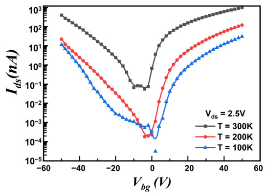
Figure 5.
Transfer curves of the MoTe2 transistor at different temperatures from 100 to 300 K at a step of 100 K.
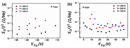
Figure 6.
(a) as function of gate voltage for p-FET and (b) for n-FET at different temperature from 100 to 300 K.
To experimentally validate the theoretical predictions, and demonstrate whether this phenomenon is occasional, several MoTe2 devices with a channel thickness ranging from 4.9 nm to 12 nm were fabricated and studied experimentally. The noise characteristics were electrically measured at different temperatures. All these experiments show the same pattern around noise characteristics. Experimental results of MoTe2 devices with a channel thickness of 8.0 nm are shown in Figure 7a,b. The same decreasing behavior of with increasing temperatures was also observed. Therefore, conductivity () of two terminals as a function of temperature was characterized to determine the conduction mechanism within the MoTe2 channel, as shown in Figure 7c. We found that the variation of with T in MoTe2 transistors can be modeled well with the variable Ids hopping (VRH) transport.
where is the threshold voltage of the device, is the total number of carriers in the conducting channel, before and after the exposures were shown in Figure 8b for p-FET and Figure 8c for n-FET, respectively. As demonstrated, for n-FET, the magnitude of noise changes increases nearly by one order, while for p-FET, it shows no apparent change, which agrees with previous studies [25,43,44,45]. For n-FET, adsorbates from ambient conditions function as trapping centers, trapping and scattering the electron within the channel, while for p-FET, the concentration of carriers will increase because of the ambient doping; thus, conductance increases and noise, in comparison, either decreases or hardly changes.
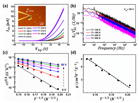
Figure 7.
Conduction mechanism in an MoTe2 transistor. (a) Transfer curves of MoTe2 FET at different temperatures from 120 to 300 K at a step of 30 K. (b) Normalized noise spectra as a function of frequency at different temperatures from 120 s to 300 K at a step of 60 K. (c) Conductivity as a function of temperature at different gate voltages ranging from 0 to 50 V at a step of 10 V. (d) Field-effect mobility of the MoTe2 transistor as a function of temperature.

Figure 8.
Impact of ambient conditions on the noise of MoTe2 transistor. (a) Transfer curves of MoTe2 FET before and after exposure to ambient conditions. (b) Hooge parameter as a function of gate voltage before and after exposure to ambient conditions for MoTe2 p-FET and (c) for MoTe2 n-FET.
4. Conclusions
In conclusion, we characterized the noise features in MoTe2 few-layered ambipolar transistors. The noise mechanism of the MoTe2 p-FET and n-FET was characterized as carrier number fluctuations, which were caused by variable range hopping transport rather than thermally activated transport in the MoTe2 conducting channel, and stayed the same with temperature. The noise of n-channel and p-channel of MoTe2 ambipolar transistors showed a different response upon exposure to ambient conditions, which indicates that n-channel transport is more sensitive to ambient conditions. These noise characteristics may provide useful guidelines to develop high-performance electronics based on the emerging transition metal dichalcogenides and can be a useful diagnostic tool to identify the conduction mechanism.
Author Contributions
Conceptualization and methodology, B.Z.; hardware, Y.X. (Youze Xin); validation, C.H., Y.L. and Y.X. (Yiyun Xie); formal analysis, Z.G. and Z.X.; investigation, B.Z.; data curation, Z.K.; writing—original draft preparation, Q.X.; writing—review and editing, C.W.; visualization, C.W.; supervision, G.Z.; project administration, L.G.; funding acquisition, B.Z. and D.L. All authors have read and agreed to the published version of the manuscript.
Funding
This research was funded by the National Natural Science Foundation of China under Grant 61874085, 62074126; by the Postdoctoral Research Funding Project of Shaanxi Province under Grant 2018BSHEDZZ41; and by the Shaanxi Key Research and Development Plan Grant 2020GY-019.
Institutional Review Board Statement
Not applicable.
Informed Consent Statement
Not applicable.
Data Availability Statement
Not applicable.
Conflicts of Interest
The authors declare no conflict of interest.
References
- Fiori, G.; Bonaccorso, F.; Iannaccone, G.; Palacios, T.; Neumaier, D.; Seabaugh, A.; Sanjay, K.; Colombo, L. Electronics based on two-dimensional materials. Nat. Nanotechnol. 2014, 9, 768. [Google Scholar] [CrossRef] [PubMed]
- Geim, A.K.; Novoselov, K.S. The structure of suspended graphene sheets. Nat. Mater. 2007, 6, 183. [Google Scholar] [CrossRef] [PubMed]
- Novoselov, K.S.; Jiang, D.; Schedin, F.; Booth, T.J.; Khotkevich, V.V.; Morozov, S.V.; Geim, A.K. Electric Field Effect in Atomically Thin Carbon Films. Proc. Natl. Acad. Sci. USA 2005, 102, 10451. [Google Scholar] [CrossRef] [PubMed] [Green Version]
- Radisavljevic, B.; Radenovic, A.; Brivio, J.; Giacometti, I.V.; Kis, A. Single-layer MoS2 transistors. Nat. Nanotechnol. 2011, 6, 147. [Google Scholar] [CrossRef] [PubMed]
- Yoon, J.; Park, W.; Bae, G.Y.; Kim, Y.; Jang, H.S.; Hyun, Y.; Lim, S.K.; Kahng, Y.H.; Hong, W.K.; Lee, B.H. Highly Flexible and Transparent Multilayer MoS2 Transistors with Graphene Electrodes. Small 2013, 9, 3295. [Google Scholar] [CrossRef]
- Ye, L.; Li, H.; Chen, Z.; Xu, J. Robust and stretchable indium gallium zinc oxide-based electronic textiles formed by cilia-assisted transfer printing. ACS Photonics 2016, 3, 692. [Google Scholar] [CrossRef]
- Das, S.; Robinson, J.A.; Dubey, M.; Terrones, H.; Terrones, M. Beyond Graphene: Progress in Novel Two-Dimensional Materials and van der Waals Solids. Annu. Rev. Mater. Res. 2015, 45, 1–27. [Google Scholar] [CrossRef]
- Li, L.; Yu, Y.; Ye, G.J.; Ge, Q.; Ou, X.; Wu, H.; Feng, D.L.; Chen, X.H.; Zhang, Y.B. Black phosphorus field-effect transistors. Nat. Nanotechnol. 2014, 9, 372. [Google Scholar] [CrossRef] [Green Version]
- Zhang, Y.J.; Ye, J.T.; Yomogida, Y.; Takenobu, T.; Iwasa, Y. Formation of a Stable p-n Junction in a Liquid-Gated MoS2 Ambipolar Transistor. Nano Lett. 2013, 13, 3023. [Google Scholar] [CrossRef]
- Yu, L.L.; Zubair, A.; Santos, E.J.G.; Zhang, X.; Lin, Y.X.; Zhang, Y.H.; Palacios, T. Transport Properties of a MoS2/WSe2 Heterojunction Transistor and its Potential for Application. Nano Lett. 2015, 15, 4928. [Google Scholar] [CrossRef] [Green Version]
- Lin, Y.L.; Xu, Y.; Wang, S.T.; Li, S.L.; Mahito, Y.; Alex, A.F.; Li, W.W.; Sun, H.B.; Shu, N.; Jian, W.B.; et al. Barrier inhomogeneities at vertically stacked graphene-based heterostructures. Adv. Mater. 2014, 26, 3263. [Google Scholar] [CrossRef]
- Koppens, F.H.; Mueller, T.; Avouris, P.; Ferrari, A.C.; Vitiello, M.S.; Polini, M. Photodetectors based on graphene, other two-dimensional materials and hybrid systems. Nat. Nanotechnol. 2014, 9, 780. [Google Scholar] [CrossRef]
- Pradhan, N.R.; Rhodes, D.; Feng, S.; Yan, X.; Balicas, L. Field-Effect Transistors Based on Few-Layered α-MoTe2. ACS Nano 2014, 8, 6. [Google Scholar] [CrossRef] [PubMed] [Green Version]
- Ruppert, C.; Aslan, O.B.; Heinz, T.F. Optical Properties and Band Gap of Single- and Few-Layer MoTe2 Crystals. Nano Lett. 2014, 14, 6231. [Google Scholar] [CrossRef] [PubMed]
- Fathipour, S.; Ma, N.; Hwang, W.S.; Protasenko, V.; Seabaugh, A. Exfoliated multilayer MoTe2 field-effect transistors. Appl. Phys. Lett. 2014, 105, 192101. [Google Scholar] [CrossRef] [Green Version]
- Chen, J.; Feng, Z.; Fan, S.; Shi, S.; Yue, Y.; Shen, W.; Xie, Y.; Wu, E.; Sun, C.; Liu, J. Contact Engineering of Molybdenum Ditelluride Field Effect Transistors through Rapid Thermal Annealing. ACS Appl. Mater. 2017, 9, 30107. [Google Scholar] [CrossRef]
- Qu, D.; Liu, X.; Ming, H.; Lee, C.; Yoo, W.J. Carrier-Type Modulation and Mobility Improvement of Thin MoTe2. Adv. Mater. 2017, 29, 1606433. [Google Scholar] [CrossRef]
- Larentis, S.; Fallahazad, B.; Movva, H.; Kim, K.; Rai, A.; Taniguchi, T.; Watanabe, K.; Banerjee, S.K.; Tutuc, E. Reconfigurable Complementary Monolayer MoTe2 Field-Effect Transistors for Integrated Circuits. ACS Nano 2017, 11, 4832. [Google Scholar] [CrossRef] [PubMed]
- Feng, Z.; Xie, Y.; Chen, J.; Yu, Y.; Zheng, S.; Zhang, R.; Li, Q.; Chen, X.; Sun, C.; Zhang, H. Highly sensitive MoTe2 chemical sensor with fast recovery rate through gate biasing. 2D Mater. 2017, 4, 025018. [Google Scholar] [CrossRef]
- Huang, H.; Wang, J.; Hu, W.; Liao, L.; Wang, P.; Wang, X.; Fan, G.; Chen, Y.; Wu, G.; Luo, W.; et al. Highly sensitive visible to infrared MoTe2 photodetectors enhanced by the photogating effect. Nat. Nanotechnol. 2016, 27, 445201. [Google Scholar] [CrossRef] [PubMed]
- Pal, A.N.; Ghatak, S.; Kochat, V.; Sneha, E.S.; Ghosh, A. Microscopic Mechanism of 1/f Noise in Graphene: Role of Energy Band Dispersion. ACS Nano 2011, 5, 2075. [Google Scholar] [CrossRef] [PubMed]
- Ghibaudo, G. Ultimately Thin Double-Gate SOI MOSFETs. SPIE 2003, 5113, 13. [Google Scholar]
- Hooge, F.N. 1/f noise sources. IEEE Trans. Electron Devices 1994, 41, 1926. [Google Scholar] [CrossRef] [Green Version]
- Lin, Y.F.; Xu, Y.; Suen, Y.W.; Yamamoto, M.; Nakaharai, S.; Ueno, K.; Tsukagoshi, K. Origin of Noise in Layered MoTe2 Transistors and its Possible Use for Environmental Sensors. Adv. Mater. 2015, 27, 6612. [Google Scholar] [CrossRef] [PubMed]
- Sangwan, V.K.; Arnold, H.N.; Jariwala, D.; Marks, T.J.; Lauhon, L.J.; Hersam, M.C. Low-Frequency Electronic Noise in Single-Layer MoS2 Transistors. Nano Lett. 2013, 13, 4351. [Google Scholar] [CrossRef] [Green Version]
- Cheng, Z.; Li, Q.; Li, Z.; Zhou, Q.; Fang, Y. Suspended Graphene Sensors with Improved Signal and Reduced Noise. Nano Lett. 2010, 10, 1864. [Google Scholar] [CrossRef]
- Renteria, J.; Samnakay, R.; Rumyantsev, S.L.; Jiang, C.; Goli, P.; Shur, M.S.; Balandin, A.A. Low-frequency 1/f noise in MoS2 transistors: Relative contributions of the channel and contacts. Appl. Phys. Lett. 2014, 104, 153104. [Google Scholar] [CrossRef] [Green Version]
- Rumyantsev, S.; Liu, G.; Stillman, W.; Shur, M.; Balandin, A.A. Electrical and noise characteristics of graphene field-effect transistors: Ambient effects, noise sources and physical mechanisms. J. Phys. 2010, 22, 395302. [Google Scholar] [CrossRef] [Green Version]
- Pellegrini, B. 1/f noise in graphene. Eur. Phys. J. B 2013, 86, 373. [Google Scholar] [CrossRef] [Green Version]
- Kumar, C.; Kuiri, M.; Jung, J.; Das, T.; Das, A. Tunability of 1/f Noise at Multiple Dirac Cones in hBN Encapsulated Graphene Devices. Nano Lett. 2016, 6, 1042. [Google Scholar]
- Levinshtein, M.E.; Pascal, F.; Contreras, S.; Knap, W.; Rumyantsev, S.L.; Gaska, R.; Yang, J.W.; Shur, M.S. AlGaN/GaN high electron mobility field effect transistors with low 1/f noise. Appl. Phys. Lett. 1998, 72, 3053. [Google Scholar] [CrossRef]
- Li, X.F.; Du, Y.C.; Si, M.W.; Yang, L.M.; Li, S.C.; Li, T.Y.; Xiong, X.; Ye, P.D.; Wu, Y.Q. Three-layer phosphorene-metal interfaces. Nanoscale 2016, 8, 3572. [Google Scholar] [CrossRef] [PubMed]
- Xie, X.X.; Sarkar, D.; Liu, W.; Kang, J.; Banerjee, K. A subthermionic tunnel field-effect transistor with an atomically thin channel. ACS Nano 2014, 8, 5633. [Google Scholar] [CrossRef]
- Ji, H.; Joo, M.K.; Yun, Y.; Park, J.H.; Lee, G.; Moon, B.H.; Yi, H.; Suh, D.; Lim, S.C. Suppression of Interfacial Current Fluctuation in MoTe2 Transistors with Different Dielectrics. ACS Appl. Mater. Interfaces 2016, 8, 19082. [Google Scholar] [CrossRef] [PubMed]
- Balandin, A.A. Two-dimensional phonon transport in graphene. Nat. Nanotechnol. 2013, 8, 549. [Google Scholar] [CrossRef] [PubMed]
- Kochat, V.; Tiwary, C.S.; Biswas, T.; Ramalingam, G.; Hsieh, K.; Chattopadhyay, K.; Raghavan, S.; Jain, M.; Ghosh, A. Magnitude and Origin of Electrical Noise at Individual Grain Boundaries in Graphene. Nano Lett. 2016, 16, 562. [Google Scholar] [CrossRef]
- Lin, Y.M.; Avouris, P. Electrical transport and 1/f noise in semiconducting carbon nanotubes. Nano Lett. 2008, 8, 2119. [Google Scholar] [CrossRef] [Green Version]
- Kim, J.K.; Song, Y.; Kim, T.Y.; Cho, K.; Pak, J.; Choi, Y.B.; Shin, J.; Chung, S.; Lee, T. Protective effects of triple fermented barley extract (FBe) on indomethacin-induced gastric mucosal damage in rats. Nat. Nanotechnol. 2017, 28, 47LT01. [Google Scholar] [CrossRef]
- Yan, S.L.; Xie, Z.J.; Chen, J.H.; Taniguchi, T.; Watanabe, K. Electrically Tunable Energy Bandgap in Dual-Gated Ultra-Thin Black Phosphorus Field Effect Transistors. Chin. Phys. B 2017, 34, 047304. [Google Scholar] [CrossRef] [Green Version]
- Delker, C.J.; Zi, Y.; Yang, C.; Janes, D.B. Current and Noise Properties of InAs Nanowire Transistors with Asymmetric Contacts Induced by Gate Overlap. IEEE Trans. Electron Devices 2013, 60, 2900. [Google Scholar] [CrossRef]
- Shklovskii, B. Dimensional quantization in a-Si:H quantum-well structures: The alloy model. Phys. Rev. B 2003, 67, 045201. [Google Scholar] [CrossRef] [Green Version]
- Qiu, H.; Xu, T.; Wang, Z.L.; Ren, W.; Nan, H.Y.; Ni, Z.H.; Chen, Q.; Yuan, S.J.; Miao, F.; Song, F.Q.; et al. Modulating the properties of MoS2 by plasma thinning and defect engineering. Nat. Commun. 2013, 4, 2642. [Google Scholar] [CrossRef] [PubMed]
- Ghatak, S.; Pal, A.N.; Ghosh, A. Nature of Electronic States in Atomically Thin MoS2 Field-Effect Transistors. ACS Nano 2011, 5, 7707. [Google Scholar] [CrossRef] [PubMed] [Green Version]
- Ishigami, M.; Chen, J.H.; Williams, E.D.; Tobias, D.; Chen, T.F.; Fuhrer, M.S. Hooge’s constant for carbon nanotube field effect transistors. Appl. Phys. Lett. 2006, 88, 203116. [Google Scholar] [CrossRef] [Green Version]
- Deen, M.J.; Marinov, O.; Holdcroft, S.; Woods, W. Low-frequency noise in polymer transistors. IEEE Trans. Electron Devices 2001, 48, 1688. [Google Scholar] [CrossRef]
Publisher’s Note: MDPI stays neutral with regard to jurisdictional claims in published maps and institutional affiliations. |
© 2022 by the authors. Licensee MDPI, Basel, Switzerland. This article is an open access article distributed under the terms and conditions of the Creative Commons Attribution (CC BY) license (https://creativecommons.org/licenses/by/4.0/).

