
Controlling Tunneling Characteristics via Bias Voltage in Bilayer Graphene/WS2/Metal Heterojunctions

 ,
, 
Abstract
:1. Introduction
2. Materials and Methods
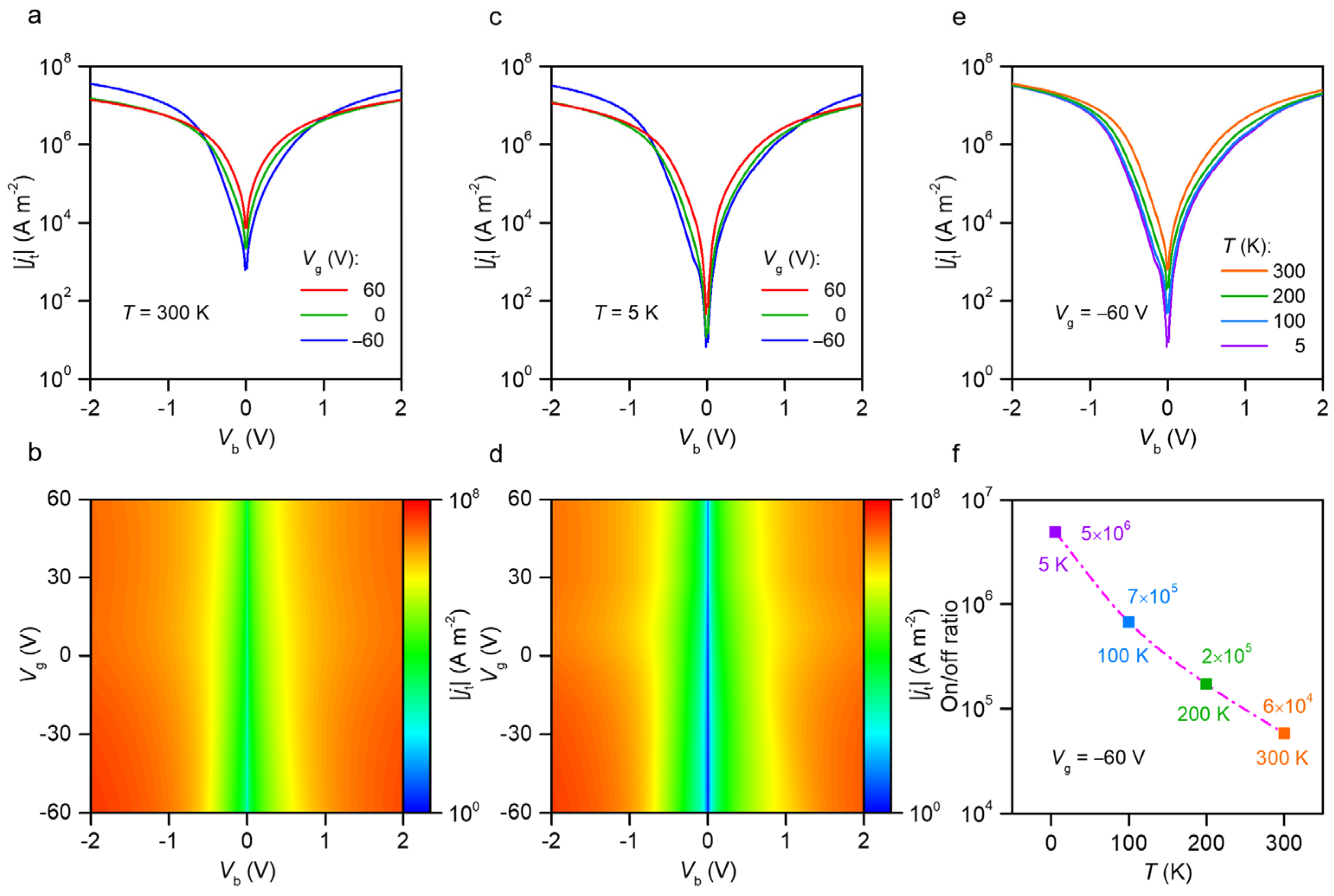
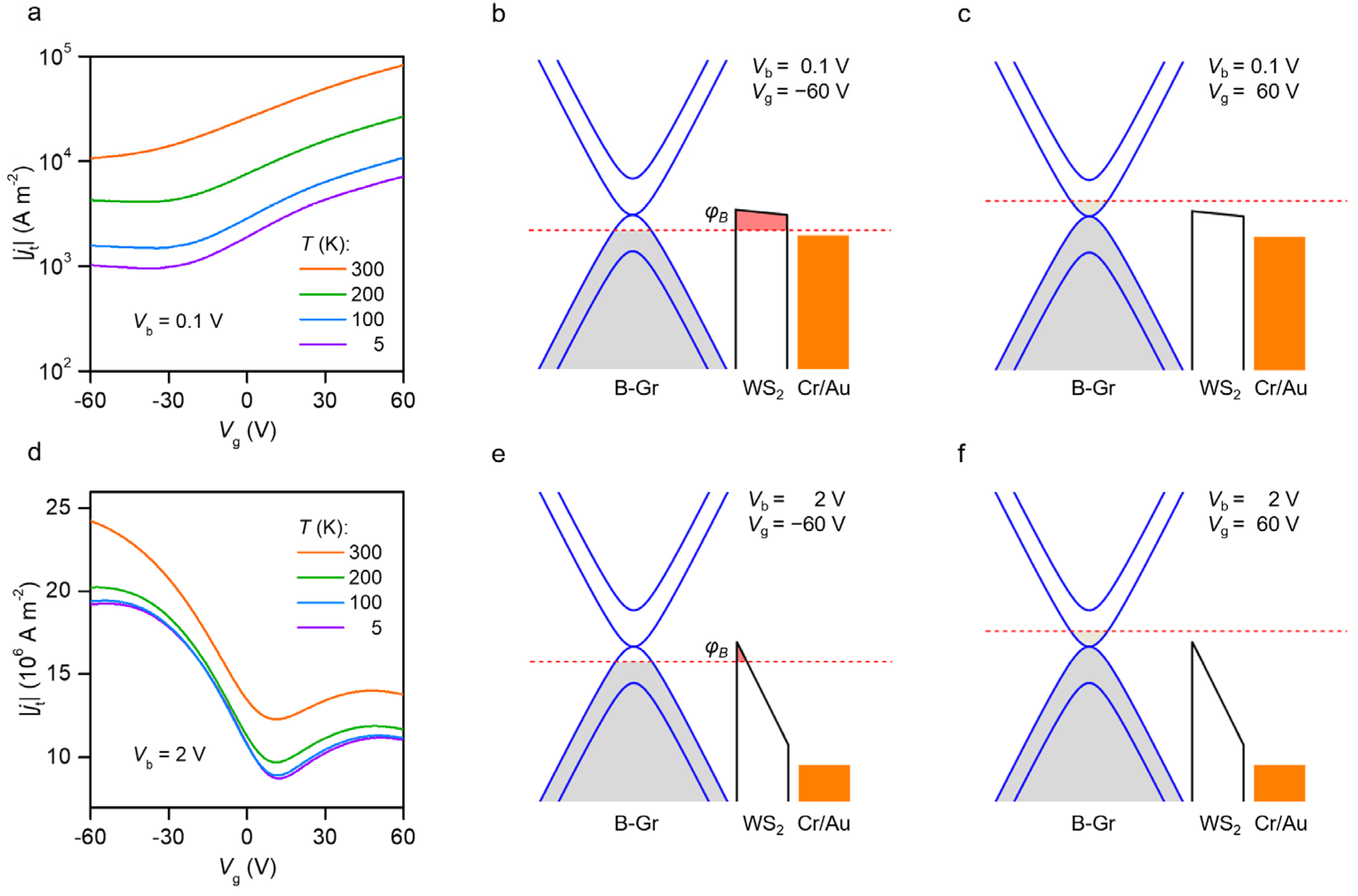
3. Results and Discussion
4. Conclusions
Author Contributions
Funding
Institutional Review Board Statement
Informed Consent Statement
Data Availability Statement
Acknowledgments
Conflicts of Interest
References
- Novoselov, K.S.; Geim, A.K.; Morozov, S.V.; Jiang, D.; Zhang, Y.; Dubonos, S.V.; Grigorieva, I.V.; Firsov, A.A. Electric Field Effect in Atomically Thin Carbon Films. Science 2004, 306, 666–669. [Google Scholar] [CrossRef] [PubMed] [Green Version]
- Graf, D.; Molitor, F.; Ensslin, K.; Stampfer, C.; Jungen, A.; Hierold, C.; Wirtz, L. Spatially resolved Raman spectroscopy of single-and few-layer graphene. Nano Lett. 2007, 7, 238–242. [Google Scholar] [CrossRef] [PubMed] [Green Version]
- Geim, A.K. Graphene: Status and prospects. Science 2009, 324, 1530–1534. [Google Scholar] [CrossRef] [PubMed] [Green Version]
- Schwierz, F. Graphene transistors. Nat. Nanotechnol. 2010, 5, 487–496. [Google Scholar] [CrossRef] [PubMed]
- Bolotin, K.I.; Sikes, K.J.; Jiang, Z.; Klima, M.; Fudenberg, G.; Hone, J.; Kim, P.; Stormer, H. Ultrahigh electron mobility in suspended graphene. Solid State Commun. 2008, 146, 351–355. [Google Scholar] [CrossRef] [Green Version]
- Neto, A.C.; Guinea, F.; Peres, N.M.; Novoselov, K.S.; Geim, A.K. The electronic properties of graphene. Rev. Mod. Phys. 2009, 81, 109. [Google Scholar] [CrossRef] [Green Version]
- Radisavljevic, B.; Radenovic, A.; Brivio, J.; Giacometti, V.; Kis, A. Single-layer MoS2 transistors. Nat. Nanotechnol. 2011, 6, 147–150. [Google Scholar] [CrossRef]
- Pradhan, N.R.; Rhodes, D.; Feng, S.; Xin, Y.; Memaran, S.; Moon, B.-H.; Terrones, H.; Terrones, M.; Balicas, L. Field-effect transistors based on few-layered α-MoTe2. ACS Nano 2014, 8, 5911–5920. [Google Scholar] [CrossRef] [Green Version]
- Fang, H.; Chuang, S.; Chang, T.C.; Takei, K.; Takahashi, T.; Javey, A. High-performance single layered WSe2 p-FETs with chemically doped contacts. Nano Lett. 2012, 12, 3788–3792. [Google Scholar] [CrossRef] [Green Version]
- Shen, P.-C.; Su, C.; Lin, Y.; Chou, A.-S.; Cheng, C.-C.; Park, J.-H.; Chiu, M.-H.; Lu, A.-Y.; Tang, H.-L.; Tavakoli, M.M. Ultralow contact resistance between semimetal and monolayer semiconductors. Nature 2021, 593, 211–217. [Google Scholar] [CrossRef]
- Iqbal, M.W.; Iqbal, M.Z.; Khan, M.F.; Shehzad, M.A.; Seo, Y.; Park, J.H.; Hwang, C.; Eom, J. High-mobility and air-stable single-layer WS2 field-effect transistors sandwiched between chemical vapor deposition-grown hexagonal BN films. Sci. Rep. 2015, 5, 1–9. [Google Scholar] [CrossRef] [PubMed] [Green Version]
- Wang, Q.H.; Kalantar-Zadeh, K.; Kis, A.; Coleman, J.N.; Strano, M.S. Electronics and optoelectronics of two-dimensional transition metal dichalcogenides. Nat. Nanotechnol. 2012, 7, 699–712. [Google Scholar] [CrossRef] [PubMed]
- Chen, J.-R.; Odenthal, P.M.; Swartz, A.G.; Floyd, G.C.; Wen, H.; Luo, K.Y.; Kawakami, R.K. Control of Schottky barriers in single layer MoS2 transistors with ferromagnetic contacts. Nano Lett. 2013, 13, 3106–3110. [Google Scholar] [CrossRef] [PubMed]
- Lin, Y.F.; Xu, Y.; Wang, S.T.; Li, S.L.; Yamamoto, M.; Aparecido-Ferreira, A.; Li, W.; Sun, H.; Nakaharai, S.; Jian, W.B. Ambipolar MoTe2 transistors and their applications in logic circuits. Adv. Mater. 2014, 26, 3263–3269. [Google Scholar] [CrossRef]
- Geim, A.K.; Grigorieva, I.V. Van der Waals heterostructures. Nature 2013, 499, 419–425. [Google Scholar] [CrossRef]
- Zhang, K.; Zhang, T.; Cheng, G.; Li, T.; Wang, S.; Wei, W.; Zhou, X.; Yu, W.; Sun, Y.; Wang, P. Interlayer transition and infrared photodetection in atomically thin type-II MoTe2/MoS2 van der Waals heterostructures. ACS Nano 2016, 10, 3852–3858. [Google Scholar] [CrossRef]
- Nourbakhsh, A.; Zubair, A.; Dresselhaus, M.S.; Palacios, T. Transport properties of a MoS2/WSe2 heterojunction transistor and its potential for application. Nano Lett. 2016, 16, 1359–1366. [Google Scholar] [CrossRef]
- Hwan Lee, S.; Sup Choi, M.; Lee, J.; Ho Ra, C.; Liu, X.; Hwang, E.; Hee Choi, J.; Zhong, J.; Chen, W.; Jong Yoo, W. High performance vertical tunneling diodes using graphene/hexagonal boron nitride/graphene hetero-structure. Appl. Phys. Lett. 2014, 104, 053103. [Google Scholar] [CrossRef] [Green Version]
- Iqbal, M.Z.; Faisal, M.M. Fowler-Nordheim tunneling characteristics of graphene/hBN/metal heterojunctions. J. Appl. Phys. 2019, 125, 084902. [Google Scholar] [CrossRef]
- Britnell, L.; Gorbachev, R.V.; Jalil, R.; Belle, B.D.; Schedin, F.; Katsnelson, M.I.; Eaves, L.; Morozov, S.V.; Mayorov, A.S.; Peres, N.M. Electron tunneling through ultrathin boron nitride crystalline barriers. Nano Lett. 2012, 12, 1707–1710. [Google Scholar] [CrossRef] [Green Version]
- Georgiou, T.; Jalil, R.; Belle, B.D.; Britnell, L.; Gorbachev, R.V.; Morozov, S.V.; Kim, Y.-J.; Gholinia, A.; Haigh, S.J.; Makarovsky, O. Vertical field-effect transistor based on graphene–WS 2 heterostructures for flexible and transparent electronics. Nat. Nanotechnol. 2013, 8, 100–103. [Google Scholar] [CrossRef] [PubMed]
- Lee, C.-H.; Lee, G.-H.; Van Der Zande, A.M.; Chen, W.; Li, Y.; Han, M.; Cui, X.; Arefe, G.; Nuckolls, C.; Heinz, T.F. Atomically thin p–n junctions with van der Waals heterointerfaces. Nat. Nanotechnol. 2014, 9, 676–681. [Google Scholar] [CrossRef] [PubMed] [Green Version]
- Yu, W.J.; Liu, Y.; Zhou, H.; Yin, A.; Li, Z.; Huang, Y.; Duan, X. Highly efficient gate-tunable photocurrent generation in vertical heterostructures of layered materials. Nat. Nanotechnol. 2013, 8, 952–958. [Google Scholar] [CrossRef] [Green Version]
- Yu, W.J.; Vu, Q.A.; Oh, H.; Nam, H.G.; Zhou, H.; Cha, S.; Kim, J.-Y.; Carvalho, A.; Jeong, M.; Choi, H. Unusually efficient photocurrent extraction in monolayer van der Waals heterostructure by tunnelling through discretized barriers. Nat. Commun. 2016, 7, 13278. [Google Scholar] [CrossRef] [PubMed] [Green Version]
- Wang, F.; Yin, L.; Wang, Z.; Xu, K.; Wang, F.; Shifa, T.A.; Huang, Y.; Wen, Y.; Jiang, C.; He, J. Strong electrically tunable MoTe2/graphene van der Waals heterostructures for high-performance electronic and optoelectronic devices. Appl. Phys. Lett. 2016, 109, 193111. [Google Scholar] [CrossRef]
- Britnell, L.; Ribeiro, R.M.; Eckmann, A.; Jalil, R.; Belle, B.D.; Mishchenko, A.; Kim, Y.-J.; Gorbachev, R.V.; Georgiou, T.; Morozov, S.V. Strong light-matter interactions in heterostructures of atomically thin films. Science 2013, 340, 1311–1314. [Google Scholar] [CrossRef] [Green Version]
- Kim, H.H.; Yang, B.; Patel, T.; Sfigakis, F.; Li, C.; Tian, S.; Lei, H.; Tsen, A.W. One million percent tunnel magnetoresistance in a magnetic van der Waals heterostructure. Nano Lett. 2018, 18, 4885–4890. [Google Scholar] [CrossRef] [Green Version]
- Cai, X.; Song, T.; Wilson, N.P.; Clark, G.; He, M.; Zhang, X.; Taniguchi, T.; Watanabe, K.; Yao, W.; Xiao, D. Atomically thin CrCl3: An in-plane layered antiferromagnetic insulator. Nano Lett. 2019, 19, 3993–3998. [Google Scholar] [CrossRef] [Green Version]
- Song, L.; Ci, L.; Lu, H.; Sorokin, P.B.; Jin, C.; Ni, J.; Kvashnin, A.G.; Kvashnin, D.G.; Lou, J.; Yakobson, B.I. Large scale growth and characterization of atomic hexagonal boron nitride layers. Nano Lett. 2010, 10, 3209–3215. [Google Scholar] [CrossRef]
- Chen, Y.; Wang, Y.; Wang, Z.; Gu, Y.; Ye, Y.; Chai, X.; Ye, J.; Chen, Y.; Xie, R.; Zhou, Y. Unipolar barrier photodetectors based on van der Waals heterostructures. Nat. Electron. 2021, 4, 357–363. [Google Scholar] [CrossRef]
- Tongay, S.; Lemaitre, M.; Miao, X.; Gila, B.; Appleton, B.; Hebard, A. Rectification at graphene-semiconductor interfaces: Zero-gap semiconductor-based diodes. Phys. Rev. X 2012, 2, 011002. [Google Scholar] [CrossRef] [Green Version]
- Kuc, A.; Zibouche, N.; Heine, T. Influence of quantum confinement on the electronic structure of the transition metal sulfide T S 2. Phys. Rev. B 2011, 83, 245213. [Google Scholar] [CrossRef] [Green Version]
- Chen, Y.; Sun, M. Two-dimensional WS 2/MoS 2 heterostructures: Properties and applications. Nanoscale 2021, 13, 5594–5619. [Google Scholar] [CrossRef] [PubMed]
- Ji, X.; Bai, Z.; Luo, F.; Zhu, M.; Guo, C.; Zhu, Z.; Qin, S. High-Performance Photodetectors Based on MoTe2–MoS2 van der Waals Heterostructures. ACS Omega 2022, 7, 10049–10055. [Google Scholar] [CrossRef] [PubMed]
- Wilson, R. Vacuum thermionic work functions of polycrystalline Be, Ti, Cr, Fe, Ni, Cu, Pt, and type 304 stainless steel. J. Appl. Phys. 1966, 37, 2261–2267. [Google Scholar] [CrossRef]
- Berkdemir, A.; Gutiérrez, H.R.; Botello-Méndez, A.R.; Perea-López, N.; Elías, A.L.; Chia, C.-I.; Wang, B.; Crespi, V.H.; López-Urías, F.; Charlier, J.-C. Identification of individual and few layers of WS2 using Raman Spectroscopy. Sci. Rep. 2013, 3, 1755. [Google Scholar] [CrossRef] [Green Version]
- Ferrari, A.C.; Meyer, J.C.; Scardaci, V.; Casiraghi, C.; Lazzeri, M.; Mauri, F.; Piscanec, S.; Jiang, D.; Novoselov, K.S.; Roth, S. Raman spectrum of graphene and graphene layers. Phys. Rev. Lett. 2006, 97, 187401. [Google Scholar] [CrossRef] [Green Version]
- Malard, L.M.; Guimarães, M.H.; Mafra, D.L.; Jorio, A. Group-theory analysis of electrons and phonons in N-layer graphene systems. Phys. Rev. B 2009, 79, 125426. [Google Scholar] [CrossRef] [Green Version]
- Wu, J.-B.; Lin, M.-L.; Cong, X.; Liu, H.-N.; Tan, P.-H. Raman spectroscopy of graphene-based materials and its applications in related devices. Chem. Soc. Rev. 2018, 47, 1822–1873. [Google Scholar] [CrossRef] [Green Version]
- Taghinejad, H.; Rehn, D.A.; Muccianti, C.; Eftekhar, A.A.; Tian, M.; Fan, T.; Zhang, X.; Meng, Y.; Chen, Y.; Nguyen, T.-V. Defect-mediated alloying of monolayer transition-metal dichalcogenides. ACS Nano 2018, 12, 12795–12804. [Google Scholar] [CrossRef]
- Simmons, J.G. Generalized formula for the electric tunnel effect between similar electrodes separated by a thin insulating film. J. Appl. Phys. 1963, 34, 1793–1803. [Google Scholar] [CrossRef] [Green Version]
- Fan, S.; Cao, R.; Wang, L.; Gao, S.; Zhang, Y.; Yu, X.; Zhang, H. Quantum tunneling in two-dimensional van der Waals heterostructures and devices. Sci. China Mater. 2021, 64, 2359–2387. [Google Scholar] [CrossRef]
- Hill, H.M.; Rigosi, A.F.; Rim, K.T.; Flynn, G.W.; Heinz, T.F. Band Alignment in MoS2/WS2 Transition Metal Dichalcogenide Heterostructures Probed by Scanning Tunneling Microscopy and Spectroscopy. Nano Lett. 2016, 16, 4831–4837. [Google Scholar] [CrossRef] [PubMed]
- Taghinejad, H.; Eftekhar, A.A.; Adibi, A. Lateral and vertical heterostructures in two-dimensional transition-metal dichalcogenides. Opt. Mater. Express 2019, 9, 1590–1607. [Google Scholar] [CrossRef]
- Levendorf, M.P.; Kim, C.J.; Brown, L.; Huang, P.Y.; Havener, R.W.; Muller, D.A.; Park, J. Graphene and boron nitride lateral heterostructures for atomically thin circuitry. Nature 2012, 488, 627–632. [Google Scholar] [CrossRef]
- Swain, G.; Sultana, S.; Parida, K. A review on vertical and lateral heterostructures of semiconducting 2D-MoS2 with other 2D materials: A feasible perspective for energy conversion. Nanoscale 2021, 13, 9908–9944. [Google Scholar] [CrossRef]


Publisher’s Note: MDPI stays neutral with regard to jurisdictional claims in published maps and institutional affiliations. |
© 2022 by the authors. Licensee MDPI, Basel, Switzerland. This article is an open access article distributed under the terms and conditions of the Creative Commons Attribution (CC BY) license (https://creativecommons.org/licenses/by/4.0/).
Share and Cite
Bai, Z.; Zhang, S.; Xiao, Y.; Li, M.; Luo, F.; Li, J.; Qin, S.; Peng, G. Controlling Tunneling Characteristics via Bias Voltage in Bilayer Graphene/WS2/Metal Heterojunctions. Nanomaterials 2022, 12, 1419. https://doi.org/10.3390/nano12091419
Bai Z, Zhang S, Xiao Y, Li M, Luo F, Li J, Qin S, Peng G. Controlling Tunneling Characteristics via Bias Voltage in Bilayer Graphene/WS2/Metal Heterojunctions. Nanomaterials. 2022; 12(9):1419. https://doi.org/10.3390/nano12091419
Chicago/Turabian StyleBai, Zongqi, Sen Zhang, Yang Xiao, Miaomiao Li, Fang Luo, Jie Li, Shiqiao Qin, and Gang Peng. 2022. "Controlling Tunneling Characteristics via Bias Voltage in Bilayer Graphene/WS2/Metal Heterojunctions" Nanomaterials 12, no. 9: 1419. https://doi.org/10.3390/nano12091419