1. Introduction
Two-dimensional (2D) layered transition metal dichalcogenides (TMDs) are emerging as candidates for novel electronic and optoelectronic devices due to their fascinating physical properties, including their large exciton binding energy, high electron mobility, and superior mechanical flexibility [
1,
2,
3,
4,
5,
6,
7,
8,
9,
10,
11,
12,
13,
14,
15,
16,
17,
18,
19,
20]. Metal electrodes are indispensable parts of all devices based on TMDs and conventional semiconductor (SC) materials [
10,
11,
12,
13]. The electrodes can inject and charge carriers into and collect charge carriers from active SC materials to operate the devices. Deposition and patterning processes of metal layers on or under ultrathin TMD layers require special care, since the physical properties of 2D TMD materials are quite distinct from those of 3D bulk counterparts [
1,
2,
3,
4,
5,
6,
7,
8,
9,
10,
11,
12,
13]. Intensive efforts based on experimental and theoretical research activities have led to proposals of useful approaches for fabrication and electrical characterization of TMD/metal contacts [
10,
11,
12,
13]. However, a universal route to achieve desirable metal contacts for TMD-based devices is still lacking [
11,
13].
There have been many successful demonstrations of high-performance optoelectronic devices that use nanopatterned metal layers [
1,
2,
3,
4,
5,
21,
22]. Patterned metal electrodes, rather than flat electrodes, can improve the light-matter interactions in SCs with the help of surface plasmons (SPs). In metal nanostructures, two types of SPs can be excited: localized surface plasmons (LSPs) and propagating surface plasmon polaritons (SPPs) [
23]. LSP effects strongly confine incident light near metal nanostructures, especially at resonance wavelengths [
1,
3,
4,
5,
6,
7]. Propagating SPP excitation at the dielectric/metal interface leads to the generation of evanescent waves perpendicular to the interface, and hence, an intense electric field appears on the metal surface [
2,
8,
21,
22]. Both LSP and SPP can boost the optical absorption in SC layers on and under metal nanostructures [
1,
2,
3,
4,
5,
6,
7,
8,
9,
21,
22]. Bottom-up and top-down techniques can be used to fabricate metal nanostructures in SC/metal hybrid systems. The former enables low-cost high-throughput fabrication but cannot produce well-ordered patterns [
1,
6,
9]. In contrast, the latter can produce regular periodic nanostructures with high precision. Electron-beam lithography is one of the most popular top-down techniques due to its high-resolution capability and compatibility with subsequent nanofabrication processes [
1,
2,
5,
7,
8]. Although the absorption coefficients of TMD materials are much larger than those of conventional SCs, the optical absorption in TMDs is limited due to their extremely small physical thickness. Thus, integration of TMDs with metal nanostructures has been attempted to overcome the limited absorption and tune the spectral response of atomically thin TMDs [
1,
2,
3,
4,
5,
6,
7,
8,
9,
14,
15,
16]. The plasmonic effects in TMD/metal nanosystems improve the performance of various TMD-based devices, including the photodetectors [
3], photocatalysis devices [
4], and bio-sensors [
5].
The optical benefits of TMD/metal nanostructures have been reported in numerous works, as discussed above. However, few studies have directly investigated the charge collection capability of metal nanostructures in TMD/metal hybrid systems. The electrical transport along the lateral direction in the TMD layers as well as that along the vertical direction at the TMD/metal interface should be considered to examine the carrier collection behaviors of the TMD/metal hybrid structures. Moreover, most TMD samples consist of micron-size flakes. Therefore, the electrical characterization of TMD-based nanostructures requires tools with a high spatial resolution. Kelvin probe force microscopy (KPFM) can measure the contact potential difference (CPD) of the sample and provide surface charge distribution with a spatial resolution of a few tens of nm [
8,
9,
13]. The CPD measurements have been used to reveal the band bending and band offset in SC heterojunctions, which can cause separation and drift of photogenerated charges in SCs [
8,
9,
24]. Light-induced CPD change is referred to as the surface photovoltage (SPV), and KPFM-based SPV measurements can be used to visualize the spatial distribution of photogenerated charge carriers in nanostructures [
25]. Thus, the KPFM characterizations will help us to study the behaviors of the charge carriers in TMD/metal hybrid nanostructures.
In this work, we fabricated MoS2/Au hybrid nanostructures and investigated their physical characteristics. SiO2 nanopillar arrays were fabricated using electron-beam lithography, and then Au thin films were evaporated onto them under high vacuum. Such patterning of SiO2 and subsequent coating of Au thin films provide a simple means of producing periodic Au nanopillars (Au-NPs). The optical spectra and calculations of the hybrid systems showed how the plasmonic Au-NPs influenced the light-matter interaction in the MoS2 monolayers transferred onto the Au-NPs. SPV characterizations of the MoS2/Au-NPs allowed us to visualize the spatial distributions of photogenerated charge carriers under light illumination.
2. Materials and Methods
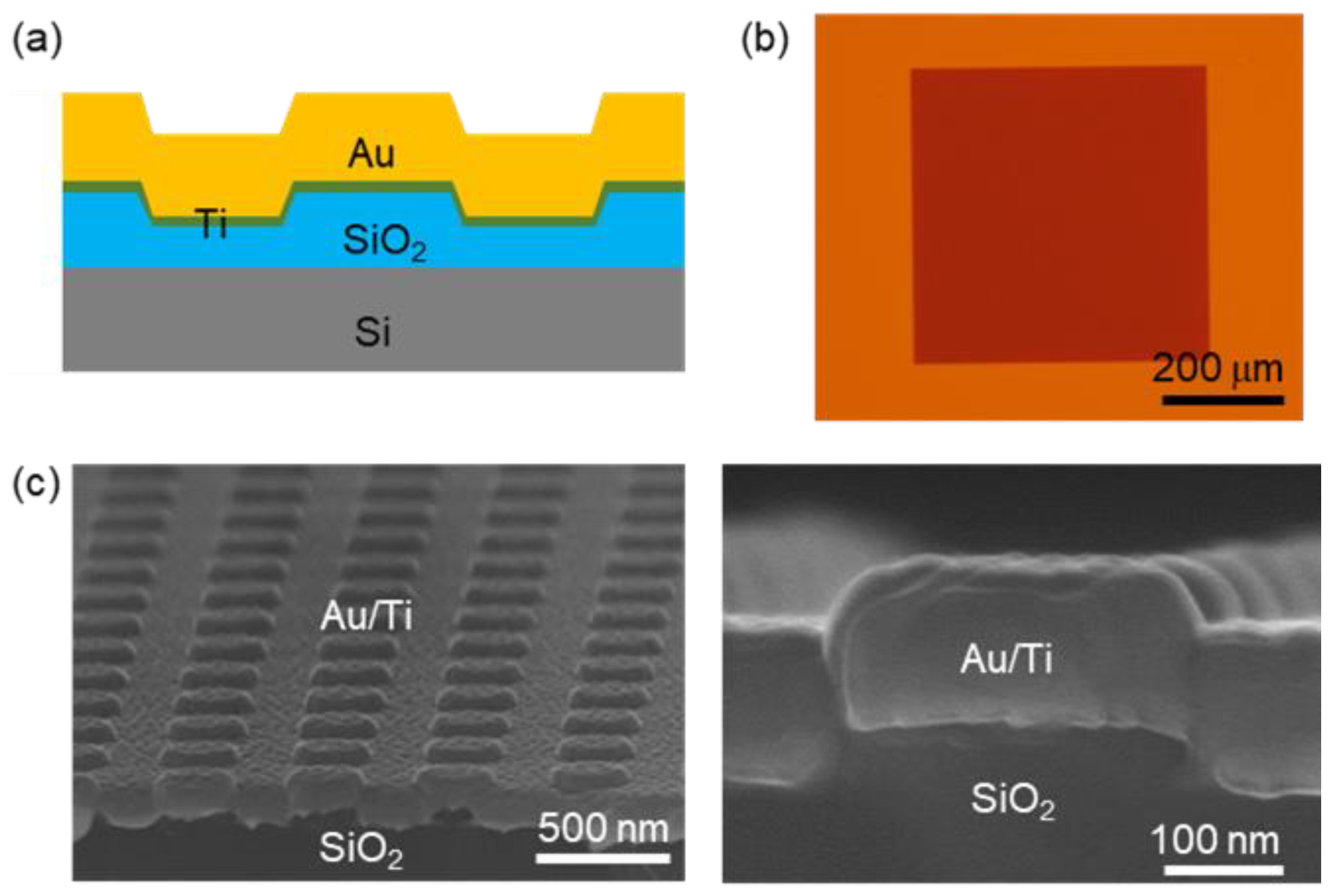
Figure 1a,b show a cross-sectional schematic diagram and a top-view optical microscope image of the Au-NP array. First, 50-nm-high SiO
2 NP arrays (period: 500 nm, top diameter: 250 nm, bottom diameter: 300 nm, and height: 50 nm) were fabricated on SiO
2 (300 nm)/Si wafers using electron-beam lithography and dry etching techniques, as reported in our earlier work [
25]. 10-nm-thick Ti adhesion layers were deposited on the SiO
2 NP arrays, and 100-nm-thick Au thin films were deposited on those layers using electron-beam evaporation. Periodic arrays of plasmonic Au-NPs can be produced through simple evaporation of Au thin films on SiO
2-NPs. The nanofabrication processes of SiO
2 are well established and widely used. Thus, the use of SiO
2-nanopattern templates provides a simple approach to obtain Au nanostructures without etching of Au thin films [
21,
22].
The area of the Au-NP array was 500 × 500 μm
2, and there was a flat region around the Au-NP array, as shown in
Figure 1b. This flat region coated with the Au/Ti thin films is referred to as Au-F, and it can be used for comparative characterizations. The low- and high-magnification scanning electron microscope (SEM) images in
Figure 1c show regular arrays of NPs and confirm the thickness of the Au (100 nm)/Ti (10 nm) films, respectively. The highly directional evaporation in our high vacuum chamber (base pressure: 10
−7 Torr) limits deposition at the NP sidewalls. Consequently, the surface morphology of Au-NPs is likely identical to that of the underlying SiO
2 NPs, as illustrated in
Figure 1a. The high-magnification cross-sectional SEM image in
Figure 1c confirms this expectation: the top and bottom diameters of the Au-NPs (250/300 nm) were almost identical to those of the SiO
2 NPs. The SEM images also show that the 100-nm-thick Au thin films formed continuous layers over the underlying SiO
2 NPs. The thickness of the Au thin film was 2 times larger than the penetration depth of Au at a wavelength (
λ) of 600 nm [
23]. Thus, the underlying SiO
2/Si substrates did not affect the optical characteristics of Au-NPs. Monolayer MoS
2 flakes grown by chemical vapor deposition were transferred onto the Au-NPs using a polymer-based wet transfer technique. Detailed procedures have been reported in our earlier publications [
8,
9]. The polymer was removed in a critical point dryer using acetone, and hence, the surface of the transferred MoS
2 flakes on Au-NPs remained very flat because the surface tension-induced strain in the suspended MoS
2 region was relieved. Optical reflectance from a selected area of several μm
2 was measured using a homemade setup consisting of an optical microscope (LV100, Nikon Instruments, Seoul, Korea), a spectrometer (Maya 2000 Pro, Ocean Insights, Rostock, Germany), and a white LED (Solis-3C, Thorlabs, Newton, NJ, USA) [
25,
26]. The measured optical spectra were compared with the calculated spectra obtained from finite-difference time-domain (FDTD) simulations (Lumerical FDTD Solutions, Vancouver, BC, Canada). The optical properties of the MoS
2 flakes were characterized using a micro-Raman and photoluminescence (PL) spectroscopy setup (XperRam C, Nanobase, Seoul, Korea) with a 532-nm-wavelength laser as a light source.
The surface morphology and CPD of the samples were simultaneously measured using atomic force microscopy (AFM) (NX10, Park Systems, Suwon, Korea) with Pt/Ir-coated Si cantilevers (NGS01/Pt, NT-MDT, Apeldoorn, The Netherlands). All the measurements were carried out in a N
2-purged glove box to avoid artefacts caused by ambient gas adsorption [
8,
9,
13]. The CPD data were obtained using the amplitude-modulation KPFM mode, where the amplitude and frequency of the AC voltage were 2 V and 17 kHz, respectively. Dark-state CPD data were obtained from the samples after they were stored in the dark for at least 1 h. Light-induced CPD changes were measured while irradiating the samples using a fiber-coupled 660-nm-wavelength light emitting diode (M660L4, Thorlabs, Newton, NJ, USA) and a focusing lens.
3. Results and Discussions
Figure 2a,b show a schematic diagram and an optical microscope image of the MoS
2 monolayer flakes transferred onto Au-F and Au-NP, respectively. Triangular-shaped flakes are clearly visible on the Au-F and Au-NP surfaces (
Figure 2b). Raman spectra of the MoS
2 flakes on Au-F and Au-NP are shown in
Figure 2c. The spacing between the in-plane (E
2g) and out-of-plane (A
1g) phonon mode peaks is 20.9 cm
−1, which confirms the preparation of monolayer MoS
2 flakes [
27]. We can note that the Raman peak spacing is identical in both MoS
2/Au-F and MoS
2/Au-NP. The Raman peak positions are sensitive to the strain states of the flakes [
17,
18,
19]. The Raman spectra show that the flakes on Au-NPs are nonstrained, similar to those on Au-F. Additionally, the Raman intensity of the MoS
2 monolayers on the Au-NPs was 3 times higher than the intensity of those on the Au-F. The peak enhancement suggests that Au-NPs could improve the optical absorption of the flakes.
Figure 3a,b show the measured and FDTD-calculated reflectance (
R) spectra of Au-F and MoS
2/Au-F, respectively.
Figure 3c,d show the measured and calculated
R spectra of Au-NP and MoS
2/Au-NP, respectively. Optical reflectance from a selected area of several μm
2 was measured using a homemade microscope-based setup [
25,
26]. When
λ was smaller than 600 nm, the measured
R values of Au-F and Au-NP decreased due to the interband transition of Au [
23]. Transfer of the MoS
2 monolayers reduced the
R of both Au-F and Au-NP, presumably due to the optical absorption in the MoS
2 flakes. The reduction in
R was more notable in the MoS
2/Au-NP than in the MoS
2/Au-F, which may indicate improved absorption in the MoS
2 flakes on Au-NP. Near
λ = 600 nm, a broad dip appeared in the measured
R of Au-NPs, and the calculated
R exhibited a much sharper dip. This reflection dip likely originated from plasmonic effects on the Au-NP surface, since such a dip was not observed in the bare SiO
2 NP array [
25]. Periodic Au nanostructures can excite propagating SPP along the surface and produce an evanescent field in a direction perpendicular to the surface [
8,
9,
21,
22,
23]. The spatial period determines the photon-SPP coupling wavelength based on the SPP dispersion relation [
23]. The Au nanogratings with a 500-nm period enable SPP excitation at
λ of 500~600 nm [
8,
9]. In the spectrum of MoS
2/Au-NP, the dip shifted again to
λ ~ 600 nm due to the large refractive index of MoS
2. This reflectance dip is close to the A and B exciton resonance wavelengths of MoS
2, as marked by the gray dashed lines in
Figure 3c,d [
28]. Therefore, the SPP-photon coupling in Au-NPs can create a large number of excitons in the MoS
2 monolayers, resulting in pronounced dips near the exciton resonance wavelengths. The discrepancies between the experimental and simulated data can be attributed to the imperfect geometric configuration and rough surface of the fabricated Au-NPs.
Figure 4a shows the PL spectra of MoS
2/Au-F and MoS
2/Au-NP. The PL intensity of MoS
2/Au-NP is 20 times larger than that of MoS
2/Au-F. It should be noted that electron transfer from MoS
2 to Au suppresses the radiative recombination of photogenerated excitons, resulting in PL quenching of the MoS
2 flakes on the flat Au thin film [
8,
9]. Consequently, the PL intensity of MoS
2/Au-F is smaller than that of MoS
2 flakes on SiO
2/Si substrates (
Supporting Information (SI), Figure S1). In the MoS
2/Au-NP, the area fraction of the suspended MoS
2 region was 4/5, and hence, only 1/5 of the area of the MoS
2 flakes remained in contact with the Au-NP top surface. This reduced contact area can prevent PL quenching; however, the area difference alone could not have led to the observed 20-fold increase in the PL intensity.
Figure 4b shows the spectra of the FDTD-calculated optical absorption in the MoS
2 monolayers (
AMoS2) on Au-NPs and Au-F.
AMoS2 could not be measured from the experiments since the Au layers and the Si substrates also absorb incident light. Thus,
AMoS2 was estimated from the FDTD simulations. Au-NPs significantly increase
AMoS2 in a broad wavelength range. In particular,
AMoS2 of the MoS
2/Au-NP at a
λ of 532 nm (the PL and Raman excitation wavelength) is 2 times larger than that of MoS
2/Au-F. The enhanced excitation should increase the Raman and PL intensities of MoS
2/Au-NP [
2,
14]. It should also be noted that the enhanced absorption near the A and B exciton resonance wavelengths of the MoS
2 monolayer was pronounced, as expected from the
R spectra. The maximum
AMoS2 of the MoS
2/Au-NP reached 60% at a
λ of 615 nm, which was 6 times larger than the
AMoS2 of the MoS
2/Au-F.
Figure 5a–c show the cross-sectional distributions of the FDTD-calculated electric field (
E) in our samples under light illumination at
λ = 530 nm, 615 nm, and 660 nm. In these calculations, the MoS
2 monolayers were assumed to have flat surfaces. The surface morphology data of the samples will be presented later. The calculated results clearly show that Au-NPs concentrate the incident light. The NP-concentrated light at
λ = 615 nm and 660 nm (the B and A exciton resonance wavelengths of the MoS
2 monolayer) is more pronounced than that at
λ = 530 nm (the Raman and PL excitation wavelengths). In fact, the
AMoS2 of the MoS
2 flake is proportional to |
E|
2 [
29]. The comparison of the |
E|
2 distributions (
Figure 5a–c) explains the wavelength dependence of the
AMoS2 of MoS
2/Au-F and MoS
2/Au-NP (
Figure 4b). The PL and Raman intensity enhancement of the MoS
2 flakes on nanostructures can be attributed to the increased electric field at the excitation and emission wavelengths [
2,
14]. The comparison of the electric field at the exciton resonance wavelengths and the excitation wavelength (530 nm) clearly suggests that the broadband enhancement of the electric field enables the increased PL and Raman intensities from MoS
2/Au-NP.
In MoS
2/Au-NP, the suspended MoS
2 flakes are above the Au thin film with a 50-nm gap. The suspended MoS
2 region can absorb reflected light from the underlying Au thin films, raising
AMoS2. As a means of enhanced absorption, insulating spacer layers, such as Al
2O
3, HfO
2, TiO
2, and SiO
2, can be inserted between the 2D TMD layers and metal back-reflectors [
15,
16]. When the Fabry–Pérot resonance condition is met, a large
E appears on the MoS
2 flake and increases the
AMoS2 [
15]. FDTD calculations showed that the optical reflectance of MoS
2 monolayers separated by a 50-nm gap above SiO
2/Si wafers was smaller than that of the MoS
2/Au-F (
SI, Figure S2). This result suggests that the gap in the Au-NP array also contributed to the enhanced optical absorption.
The surface morphology (top) and the line profile of topography (bottom) shown in
Figure 6a indicate that the MoS
2 monolayer flakes transferred onto the Au-NP array had very flat surfaces. This result suggests that the nonstrained MoS
2 monolayers were suspended between neighboring Au-NPs. Since the surface morphology of the MoS
2 flakes did not undergo severe deformation, it was very difficult to distinguish the MoS
2/Au-NP contact region from the suspended region of the surface morphology (
Figure 6a). As shown in
Figure 1c, the evaporated Au thin films had a rough surface, resulting from migration and agglomeration during growth [
15]. In
Figure 6a, characteristic features of the agglomerated Au surface can be observed on the MoS
2 surface, allowing us to identify the MoS
2/Au-NP contact region (yellow dashed line circles).
Figure 6b shows the maps and histograms of the measured CPD in MoS
2/Au-NP, respectively. The average CPD in the MoS
2/Au-NP contact region and the suspended MoS
2 region were estimated by fitting the histograms with two Gaussian functions. The estimated CPD
D in the MoS
2/Au-NP contact region was 85 mV larger than that in the suspended regions. As shown in the topographic image (
Figure 6a) and the Raman spectra (
Figure 2c), the MoS
2 monolayer flakes were suspended on Au-NPs without strain. Thus, the CPD
D modification likely originated from the strong electronic interactions at the interface of MoS
2 and Au. Overlap of the wavefunctions and the resulting electron redistribution at the interfaces lead to electronic dipoles and increase the CPD
D [
13]. A larger CPD
D corresponds to a larger electric potential, and hence, the electric potential in the MoS
2/Au-NP contact region is higher than that in the suspended MoS
2 region.
Nanostructures with high aspect ratios greatly deform the surface morphology of the MoS
2 flakes on them, and the local strain modifies the electronic structure of the flake [
9,
17,
18,
19]. Tensile strain decreases the bandgap energy of TMD monolayers and increases the local density of excitons in the strained region [
17,
18,
19]. Such strain engineering enables researchers to create wavelength-tunable light emitters [
17] and quantum emitters [
18,
19]. Therefore, both strain effects should be used to explain the physical characteristics of TMD/metal hybrid nanostructures. The electronic interaction at the MoS
2/Au interface increased the CPD of the MoS
2 surface, as discussed above. However, the local strain imposed by the nanostructures reduced the CPD of the MoS
2 flake on them [
9]. In MoS
2/Au-NP, the preparation of nonstrained MoS
2 flakes led to clear CPD contrast, as shown in
Figure 6b.
The first dark-state CPD (CPD
D) maps were obtained after the sample was stored in the dark for at least 1 h, and the CPD under light illumination (CPD
L) maps was measured while the sample was irradiated with 660-nm-wavelength light. The wavelength of the light source was identical to the A exciton resonance wavelength of the MoS
2 monolayer (
Figure 4b). Under light illumination, the overall CPD
L became larger than the CPD
D, indicating positive surface charging (
Figure 6b) [
24]. The SPV signals (≡ CPD
L − CPD
D) were estimated to be 31 mV and 28 mV in the MoS
2/Au-NP contact region and the suspended MoS
2 region, respectively. This result suggests that the Au-NPs collected the photogenerated electrons from the whole MoS
2 flake. In contrast, the SPV of MoS
2/Au-F was only several mV under identical measurement conditions (
SI, Figure S3). The much larger SPV signals in MoS
2/Au-NP were attributed to the significantly enhanced optical adsorption and the efficient collection of the charge carriers from the suspended MoS
2 regions.
Plausible scenarios to explain all the experimental results are illustrated in
Figure 6c. The photogenerated excitons in the MoS
2/Au-NP contact region can be separated by the aforementioned interfacial electric dipole, and the electrons are readily transferred to Au-NPs. The dipole formation raised the electric potential at the MoS
2/Au contact, leading to a large potential gradient around Au-NPs. Such a potential difference is clearly shown in the CPD
D map in the dark (
Figure 6b), which can drive the separation of excitons and the subsequent drift of electrons towards the Au-NPs. Therefore, positive charging occurs at not only MoS
2/Au-NP contacts but also in the suspended MoS
2 regions. After the light source was turned off, the measured CPD
D returned to the value of the initial dark state (
SI, Figure S4). This suggests that either desorption or chemical reaction on the sample surface cannot explain the measured CPD changes. In
Figure 6c, radiative recombination processes are not included for the sake of simplicity.


 ,
, 