Abstract
Charge injection and transport interlayers play a crucial role in many classes of optoelectronics, including organic and perovskite ones. Here, we demonstrate the beneficial role of carbon nanodots, both pristine and nitrogen-functionalized, as electron transport materials in organic light emitting diodes (OLEDs) and organic solar cells (OSCs). Pristine (referred to as C-dots) and nitrogen-functionalized (referred to as NC-dots) carbon dots are systematically studied regarding their properties by using cyclic voltammetry, Fourier-transform infrared (FTIR) and UV–Vis absorption spectroscopy in order to reveal their energetic alignment and possible interaction with the organic semiconductor’s emissive layer. Atomic force microscopy unravels the ultra-thin nature of the interlayers. They are next applied as interlayers between an Al metal cathode and a conventional green-yellow copolymer—in particular, (poly[(9,9-dioctylfluorenyl-2,7-diyl)-alt-co-(1,4-benzo-{2,1′,3}-thiadiazole)], F8BT)—used as an emissive layer in fluorescent OLEDs. Electrical measurements indicate that both the C-dot- and NC-dot-based OLED devices present significant improvements in their current and luminescent characteristics, mainly due to a decrease in electron injection barrier. Both C-dots and NC-dots are also used as cathode interfacial layers in OSCs with an inverted architecture. An increase of nearly 10% in power conversion efficiency (PCE) for the devices using the C-dots and NC-dots compared to the reference one is achieved. The application of low-cost solution-processed materials in OLEDs and OSCs may contribute to their wide implementation in large-area applications.
1. Introduction
In 1987, Tang and Van Slyke introduced the first electroluminescent device based on organic semiconductors, the so-called organic light emitting diode (OLED) [1]. After three decades, they are considered a mature technology and have already achieved successful market entry. However, OLEDs still attract research interest because of their potential as a promising technology for solid state lighting and flat panel displays [2], considering their low-cost fabrication, flexibility and large viewing angle. The balance of charge injection and the transport of holes and electrons through the organic semiconductor plays a vital role regarding the device’s (OLED and OSC) efficiency [3]. One of the key issues for the efficient design of organic optoelectronic devices is the understanding of the energy-level alignment at the metal contact/organic semiconductor interfaces. Proper matching of the electrode Fermi level to the energy level of the charge transport states of the organic semiconductor is necessary to obtain efficient and balanced charge injection in these organic electronic devices [4]. This is why, in highly efficient devices, anode and cathode interfacial layers are necessary to enhance the charge exchange between metal contacts and organic molecules.
A typical structure of an OLED and/or OSC is based on a multilayer architecture [5]. The emissive and/or photoactive layer and the various interlayers (hole injection layers (HILs), hole transport layers (HTLs), electron blocking layers (EBLs), hole blocking layers (HBLs), electron transport layers (ETLs) and electron injection layers (EILs)) are sandwiched between the two electrodes (anode and cathode). It is well known that in organic electroluminescent devices, the mobility of holes is larger than that of electrons and the hole injection barrier is lower than the electron injection barrier [6]. Such devices have extra holes in the emission region, and electrons are more or less consumed before reaching the emissive layer, which decreases the device’s efficiency. An effective approach is to modify the cathode, aiming to reduce the energy barrier and increase the charge transport between the metal cathode and the emissive and/or photoactive layer. This can be accomplished by inserting suitable interfacial layers (ETL, HBL, EIL) [7,8]. A large number of organic and inorganic materials have been applied as ETLs in OLEDs and OSCs to lower the electron injection barrier and achieve charge carrier balance. They include transition metal oxides with intrinsic n-type conductivity, such as zinc oxide (ZnO) [9,10,11,12] and tin dioxide (SnO2) [13,14], and mostly organic molecules bearing suitable functional groups, such as perylene [15,16] and porphyrin [17,18,19] compounds, polymeric oxadiazoles, metal chelates, azole-based materials and triazine [20,21,22,23,24,25]. However, despite their great success, many of these materials require vacuum deposition methods, which are incompatible with large-area devices for low-cost applications. The development of solution-processable materials of potentially low cost and with facile synthesis and deposition methods still represents a topic of intense research interest in OLEDs and OSCs.
Carbon nanodots are advantageous in terms of the abundant and sustainable precursor materials and facile surface functionalization to promote their beneficial properties. The facile and low-cost preparation/modification of these materials motivated us to further explore their use as ETLs in high-performance green emitting OLEDs and inverted OSCs. We synthesized pristine and nitrogen-functionalized carbon dots (described hereafter as C-dots and NC-dots, respectively) and unraveled their effects on the OLED and OSC performance, which paves the way for the further exploration of not only organic but also perovskite optoelectronics.
2. Materials and Methods
2.1. OLED Device Fabrication Procedure
The first and most fundamental step before performing the layers’ deposition was the proper cleaning of the glass substrates. We utilized coated glass substrates of indium-tin oxide (ITO) purchased from Sigma-Aldrich (Athens, Greece), with sheet resistance of 15–25 Ω/sq, which served as the transparent anode electrode. ITO-coated glasses were placed into an ultrasonic cleaner, where they remained for ten minutes in each bath: first in deionized water, then in acetone and finally in isopropyl alcohol (IPA). Moreover, all samples were dried with N2 gas before each bath. Then, the ITO substrates were subjected to UV–ozone treatment for 20 min. Next, we performed the deposition of hole injection layers (HTLs) using the commercially available solution PEDOT:PSS (poly(3,4 - ethylenedioxythiophene)−poly(styrenesulfonate)) with 1.3 wt % dispersion in H2O, from Sigma-Aldrich. At first, it was passed through a 0.45 μm pore diameter polyvinylidene fluoride (PVDF) filter and then was spin-coated on ITO-coated glass substrates at 6000 rpm for 40 s, forming a 40 nm thick layer. The substrates were annealed at 110 °C for at least 30 min on a hotplate. A green-yellow copolymer, named F8BT (poly[(9,9-dioctylfluorenyl-2,7-diyl)-alt-co-(1,4-benzo-{2,1′,3}-thiadiazole)), purchased from the American Dyes Source, Quebec, Canada, (ADS 233 YE), used as the emissive layer. F8BT was filtered through a 0.22 μm pore diameter PTFE filter and was deposited on top of the PEDOT:PSS. The deposition was carried out by spin-coating at 1200 rpm for 40 s from a 10 mg mL−1 solution in chloroform, forming a 80 nm thick layer. The substrates were annealed at 85 °C for 10 min on a hotplate. Moreover, carbon dots were employed as EILs. In particular, 50 μL of carbon dots (C-dots) and nitrogen-doped carbon dots (NC-dots) was spin-coated at 2000 rpm for 40 s from a 0.5 mg mL−1 solution in methanol atop the emissive layer. Finally, the OLED devices were completed with the deposition of a 150 nm aluminum layer through thermal evaporation in order to serve as the cathode electrode. The active surface of each diode was set at 12.56 mm2.
2.2. OSC Device Fabrication Procedure
Glass/ITO substrates were cleaned as already mentioned and used as the transparent cathode electrode for the fabrication of the inverted OSCs. Tin oxide purchased from Alfa Aesar was deposited from a water solution (15% colloidal dispersion of tin(vi) oxide in deionized water was diluted in 1:6.5 water) with spin-coating at 3000 rpm for 30 s. Then, the samples were thermally annealed at 150 °C for 30 min. PTB7-Th:PCBM (purchased from Ossila, Sheffield, UK), at 10 mg:15 mg in 1 mL 1,2-dichlorobenzene with the addition of 3% per volume 1,8 diiodoctane (DIO), was spin-coated at 1000 rpm for 90 s on the SnO2 ETL to serve as the photoactive layer. The fabrication procedure was completed with the deposition of molybdenum oxide (MoOx) HTL by a hot-wire CVD method [26] and Al anode electrode by thermal evaporation.
2.3. Characterization Methods
Current density–voltage–luminance (Ι−V−L) measurements were performed using a Keithley 2601A Power Supply Source-Meter (Vector Technologies, Athens, Greece) in voltage mode, with constant increment steps. The instrument was used both for slow (delay time of 1 sec before each measurement point) and fast (delay time of <1 msec) measurements. EL analysis was performed using a calibrated photodiode (BPW34 Si PIN photodiode) (Vector Technologies, Athens, Greece) connected to a Keithley 6500 DMM (Vector Technologies, Athens, Greece). The same instruments were used for the current and luminance–time (I-t and L-t) measurements. In this case, the current measurements through the diodes were acquired at rates of up to 1K sample/sec, while the luminance values were obtained at faster rates, reaching values of up to 1M sample/sec. All measurements were performed at room temperature in a dark shielded probe station to minimize light and EM interference. For the OSCs’ electrical characterization in dark and illuminated conditions, a Keithley 2400 source meter unit and a Xe lamp with an AM 1.5G filter were used. TEM measurements were performed using a Philips CM 20 transmission electron microscope (Thermo fisher scientific, United States). UV–Vis absorbance and transmittance spectra were captured by a Perkin Elmer Lambda 40 UV–Vis spectrometer (Vamvakas-Scientific Equipment, Athens, Greece). XRD patterns were recorded using a Smart Lab Rigaku diffractometer (Japan) with Cu Kα radiation. Cyclic voltammetry measurements were performed using a VersaSTAT 4 potentiometer (Megalab SA, Athens, Greece). Fourier-transform infrared (FT-IR) spectroscopy was performed using a Bruker Tensor 27 spectrometer (Interactive, Athens, Greece), with a DTGS detector. The surface morphology of devices was recorded with an NT-MDT AFM system (LaborScience SA, Athens, Greece) in tapping operation mode. Ellipsometry measurements were carried out with a J.A Woolam Inc. M2000F rotating compensator ellipsometer that operated within the 250–1000 nm range, running the WVASE32 software, at an angle of incidence of 75.14°. Steady-state PL measurements were performed with a commercial platform (ARKEO—Cicci Research). In particular, the substrate was illuminated with a diode-pumped solid-state Nd:YVO4 + KTP laser (peak wavelength 532 nm ± 1 nm, optical power 1 mW on a circular spot of 2 mm of diameter 31 mW cm−2) at an inclination of 45°. The fluorescence on the opposite side of the substrate was focused on a bundle of fibers (10 mm in diameter) with an aspheric lens close to the substrate to maximize the PL. The bundle sent the signal to a CCD-based spectrometer. The integration time and the number of averages was maintained to better compare the results. Time-resolved PL (TRPL) spectra were measured with an FS5 spectrofluorometer from Edinburgh Instruments (Livingston, UK). A 478.4 nm laser was used as an excitation source. All measurements were performed in environmental conditions at room temperature.
3. Results and Discussion
3.1. Characterization of Carbon Dots and F8BT/Carbon Dot Interfaces
In this work, we studied carbon and nitrogen-functionalized carbon nanodots that were synthesized by a bottom-up approach from inexpensive, organic precursors; their design was based on sodium carboxylate groups and carboxylic acid with amino-terminated groups, respectively. The surface terminal groups of the synthesized carbon dots (C-dots) and nitrogen-doped carbon dots (NC-dots) are illustrated in Figure 1a. They were both processed from solutions in orthogonal to organic semiconductor solvents, such as methanol and dimethylformamide (DMF).
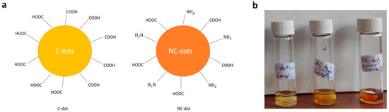
Figure 1.
(a) Illustration of the chemical structures (surface functionalization) of C-dots and NC-dots. (b) Photographs demonstrating the solution processability of carbon nanodots. From left to the right: a methanol solution of C-dots, a methanol solution of NC-dots and a DMF solution of NC-dots.
The morphology and structure of these nanodots and carbon dots were investigated by transmission electron microscopy (TEM). Figure 2a shows a TEM image of the C-dots, suggesting the formation of uniform spherical particles with an average size of around 3 nm. The crystallinity of the nanodots was studied by X-ray diffraction (XRD) measurements. Figure 2b,c show the XRD patterns of thin film deposited from C-dot and NC-dot solutions, respectively. In the case of C-dots, the only peak that appeared was assigned to the silicon substrate; therefore, the sample was amorphous. However, the diffraction pattern of NC-dots consisted of more intense peaks that revealed the formation of a more crystalline structure in these dots. As represented in Figure 2c, the XRD pattern of the NC-dots included peaks at 2θ = 20.9°, 28.7°, 39.0° and 61.6°. The corresponding Miller indices according to the relevant literature are also shown in Figure 2c,d [27]. Notably, XRD revealed that the NC-dot sample was more crystalline compared to the pristine C-dots. The lattice d-spacing was found to be 0.31 nm. This could be beneficial for electron transport when these materials are used as cathode interfacial layers in organic optoelectronic devices. Figure 2d depicts the UV–Vis absorption spectra and the derived Tauc plot for the estimation of the energy bandgap (EG) values of these materials. The extracted values are 2.6 eV for C-dots and 2.3 eV for the NC-dots.
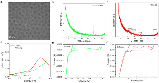
Figure 2.
(a) Transmission electron microscopy (TEM) images of carbon dots. XRD patterns of (b) C-dot and (c) NC-dot films drop cast on silicon substrates from concentrated (10 mg mL−1) methanol solutions. (d) Tauc plots of C-dot and NC-dot films drop cast onto quartz substrates from concentrated (10 mg mL−1) methanol solutions. Cyclic voltammetry of (e) C-dot and (f) NC-dot films coated on indium-tin oxide (ITO)/glass substrates at a scan rate of 0.1 V s−1 in a 0.1 M LiClO4 aqueous electrolyte solution.
Amino groups have been considered beneficial for use in EILs as they usually induce the formation of negative interfacial dipoles at the cathode interface [28]. As a result, they can reduce the electron injection barrier at the respective contact. Therefore, it is of significant importance to estimate the energy levels of the synthesized materials and obtain valuable information about the energetic alignment at the cathode interface. As cyclic voltammetry is considered one of the most powerful tools to investigate the reduction and oxidation processes of molecular species, we employed this method to estimate the highest occupied molecular orbital (HOMO) and lowest unoccupied molecular orbital (LUMO) energy levels of these materials. Figure 2e,f show the cyclic voltammograms of C-dot and NC-dot films, respectively, deposited on indium-tin oxide (ITO)/glass substrates.
Oxidation and reduction processes are represented, allowing the HOMO and LUMO calculation, respectively, using the empirical formulas [29,30]:
where Eox,onset and Ered,onset are the oxidation and reduction potential onset, respectively, defined as the position where the current starts to differ from the baseline. From the cyclic voltammograms the extracted Eox,onset value is +1.2 V and +1.8 V for C-dots and NC-dots, respectively, which results in HOMO levels of −5.6 eV for C-dots and −6.2 eV for NC-dots. The LUMO levels of C-dots and NC-dots are −3.4 eV and −3.5eV, respectively, determined by the reduction potential onset (−1 V for C-dots and −0.9 V for NC-dots).
EHOMO = −(Eox,onset + 4.4) eV
ELUMO = −(Ered,onset + 4.4) eV
The deposited films were further characterized by Fourier-transform infrared spectroscopy (FT-IR) in order to recognize any possible changes in the F8BT film after the deposition of C-dots and NC-dots (Figure 3). In the C-dot spectrum, the broad band observed in the range of 3500-3100 cm−1 corresponds to the stretching vibration of the O–H bond, while the weak band at 2930 cm−1 corresponds to C–H stretching. The two bands at 1560 cm−1 and 1395 cm−1 correspond to the asymmetric and symmetric stretching of the carboxylate group. In the case of the NC-dot spectrum, the stretching modes of N–H, O–H and C–H are detected in the broad band ranging from 3600 cm−1 to 2800 cm−1. The other bands detected at 1700 cm−1, 1650 cm−1 and 1560 cm−1 refer to the C=C stretching mode, the C=O stretching mode and the N-H bending mode, respectively.
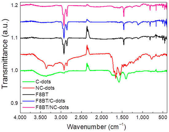
Figure 3.
FTIR spectra of pristine carbon dots and F8BT films and of F8BT/C-dot and F8BT/NC-dot interfaces.
As far as the spectrum of the F8BT emitter is concerned, the bands at 2930 cm−1 and 2850 cm−1 correspond to the stretching mode of the C–H bond, while the band at 1460 cm−1 is due to the C=C stretching mode of an aromatic group [31,32]. Furthermore, the stretching mode between the phenyl rings is detected at 1250 cm−1, the deformation of aliphatic chain bonds at 1100 cm−1 and the C–H rocking mode at 812 cm−1. In the case of the F8BT films with C-dots deposited on top, a slight increase in the intensity and width of the band at 1100 cm−1 is observed, with no other obvious changes. When NC-dots are deposited on top of a F8BT film [32], a similar change is apparent in the 1100 cm−1 region, where the band corresponding to aliphatic chain deformation almost disappears. This is a sign of possible interaction between the aliphatic chains of the F8BT molecule and the NC-dot material deposited on top. However, the bands corresponding to the stretching vibrations of the same aliphatic chains do not change, which is an indication of the limited extent of this interaction.
We next investigated the optoelectronic and morphological properties of F8BT before and after coverage with thin carbon dot interlayers (processed from 0.5 mg mL−1 in methanol solutions). In Figure 4a, the UV−Vis absorption spectra of F8BT without and with carbon dots spin-coated are presented. All these spectra exhibit absorption peaks centered at wavelengths of 372 nm and 450 nm, corresponding to F8BT [33]. The characteristic carbon dot absorption peaks were not detected in layers deposited on top of the F8BT, which is an indication that they form very thin interlayers on top of F8BT.
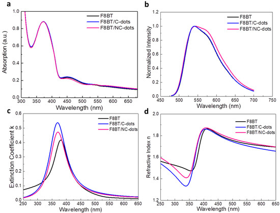
Figure 4.
(a) UV–Vis absorption and (b) steady-state PL spectra of F8BT pristine and coated with C-dots and NC-dots. (c) Extinction coefficient and (d) refractive index measurements of F8BT and F8BT/C-dot and F8BT/NC-dot interfaces.
Moreover, the emission characteristics of the same samples were investigated by measuring the steady-state photoluminescence (PL) spectra (Figure 4b). While the spectra of F8BT and F8BT/C-dots are identical, a shoulder observed at approximately 580 nm for the F8BT/NC-dot sample can be attributed to an interaction between the aliphatic chains of the F8BT molecule and the NC-dot interlayer, as already discussed in the FT-IR measurements. In addition, no changes in the time-resolved photoluminescence (TRPL) spectra (Figure S1, Supplementary Materials) of pristine and nanodot-coated F8BT films are observed, exhibiting similar average lifetimes in all cases. However, the extinction coefficients and refractive indices (RI) of F8BT pristine and coated with carbon dots present some changes (Figure 4c,d). In particular, a change in the RI may be an indication that the insertion of these dots can change the light outcoupling efficiency of the fabricated OLEDs. Such change, however, is expected to be rather marginal since the difference in RI is very small at the emission wavelength range of F8BT (centered on 530 nm). Notably, the carbon dot interlayers induce a small increase in the surface roughness of F8BT, as indicated by the similarity of the atomic force microscopy (AFM) surface topography of these samples (Figure 5). A small increase in surface roughness or the formation of small nanostructures may be beneficial for the device performance as they enlarge the area, where electron injection towards the emissive layer occurs [34,35,36].
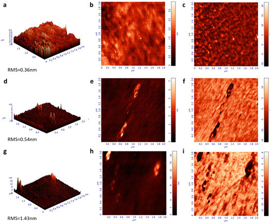
Figure 5.
Atomic force microscopy (AFM) surface topographies (height, 3D-left and 2D-middle, phase-right) of (a–c) F8BT, (d–f) F8BT/C-dot and (g–i) F8BT/NC-dot films.
3.2. OLED Measurements
To demonstrate the practical utility of these solution-processed carbon nanodots, we next applied them as EIL/ETLs in fluorescent OLEDs based on a green-yellow fluorescent polymer, well known as F8BT. The accurate structure of the OLEDs is represented in Figure 6a. Specifically, the devices consisted of indium-tin oxide (ITO) coated glass substrates as the transparent anode electrode, poly(3,4-ethylenedioxythiophene) polystyrene sulfonate (PEDOT:PSS) as the hole transport layer, F8BT as the emissive layer, C-dots or NC-dots as the electron transport layers and Al contact as the cathode electrode. A reference device using a commonly used solution-processed EIL, namely cesium carbonate (Cs2CO3), was also fabricated. The corresponding energy level diagram of the materials embedded into the OLED structure, as well as the chemical structure of F8BT, is illustrated in Figure 6b. Note that the work functions of ITO, PEDOT:PSS and Al, along with the energy levels of F8BT, were taken from the literature [37,38]. The HOMO and LUMO levels of both carbon nanodots were estimated by cyclic voltammetry and optical measurements, as already mentioned.
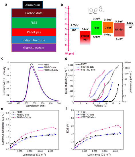
Figure 6.
(a) The OLED architecture and (b) the corresponding energy level diagram. The chemical structure of the F8BT is also presented. (c) Electroluminescence (EL) spectra of the different devices at a voltage of 5 V. (d) Current density (solid symbols)–voltage and luminance (open symbols)–voltage characteristics of the three types of OLEDs. (e) Luminous efficiency (LE) and (f) external quantum efficiency (EQE) of the same devices.
Figure 6c shows the electroluminescence (EL) spectra of the three different types of devices. It becomes obvious that the devices with C-dots and NC-dots do not affect the spectral dependence of the emission, which originates only from F8BT. Figure 6d illustrates a plot of the current density versus the applied voltage and luminance versus the applied voltage of the OLEDs. Devices with C-dots and, especially, those using NC-dots have a rapid increase in the current density at the low-voltage regime—an indication of the reduced electron injection barrier in these devices compared to the reference one. Furthermore, from the plot of luminance versus the applied voltage of these OLEDs, the device turn-on voltage (VON, the voltage where the luminance becomes equal to 1 cd m−2) can be estimated. For the reference device, the VON is calculated to be around 8 V, whereas it is decreased to nearly 6 V and further to 4 V for the devices using C-dots and NC-dots, respectively, indicating the crucial role of the carbon dots in the device performance. Figure 6e,f present the luminous efficiency (LE) and external quantum efficiency (EQE) of the prepared OLEDs, where a clear enhancement in the device performance is observed when nanodots, especially NC-dots, are incorporated in the device. In particular, the NC-dot-based OLED exhibits a ~1.5 fold higher LE and EQE compared with the reference device. A small enhancement in hydrophobicity induced by the coverage of F8BT with the carbon nanodots (Figure S2, Supplementary Materials) is also observed, which could be beneficial in the device’s stability.
Furthermore, to unambiguously demonstrate the beneficial effect of these carbon dots for OLEDs, mainly due to a reduction in the electron injection barrier, we fabricated electron-only devices and measured the carrier obtained by blocking one type of carrier (holes) through the absence of the hole injection layer (PEDOT:PSS) at the anode side of the device. Figure 7 shows the current density taken in electron-only devices using either Cs2CO3 or the newly developed carbon nanodots at one side of the device. By considering that the bulk-limited currents are similar to these devices, the obtained current densities are governed by electrode-limited processes (electron barriers are responsible for conduction) [16,39]. As shown in Figure 7, the current density versus voltage (J-V) curve of the reference diode (shown in a semilog plot) is always lower compared to the current densities of the carbon dots using diodes, a clear indication that the electron injection barrier is reduced upon the application of carbon nanodots, especially those with the amino-functionalized surface, as cathode interlayers in these devices.
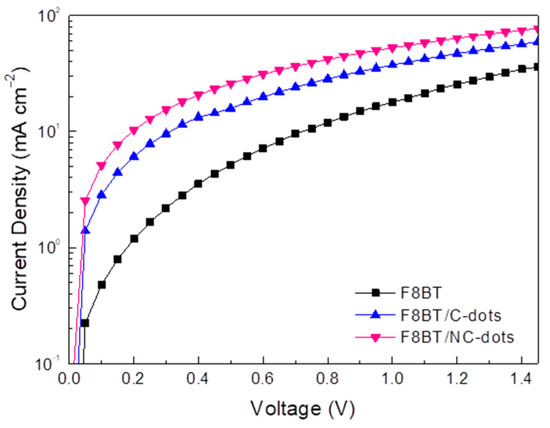
Figure 7.
Electron-only current densities of diodes with the structure ITO/F8BT/Al without and with C-dots and NC-dots at the cathode side of the device.
3.3. OSC Measurements
In order to strengthen our approach, we also employed the nanodots as cathode interlayers in inverted OSCs based on a PTB7-Th (poly[4,8-bis(5-(2-ethylhexyl)thiophen-2-yl)benzo[1,2-b;4,5-b’]dithiophene-2,6-diyl-alt-(4-(2-ethylhexyl)-3-fluorothieno[3,4-b]thiophene-)-2-carboxylate-2-6-diyl)]) donor and PCBM ([6,6]-phenyl-C61-butyric acid methyl ester) acceptor blended photoactive layer. Figure 8a illustrates the device structure of the fabricated inverted OSCs, while Figure 8b presents the chemical structure of the donor and acceptor materials that constituted the photoactive layer. Carbon nanodots spin-coated from a methanol solution with a concentration of 0.5 mg mL−1 on tin oxide (SnO2) were used as ETLs, forming an ultra-thin film to improve the electron transport between the cathode and the photoactive layer. Note that molybdenum oxide (MoOx), used as a hole transport layer, and a reference device without the nanodots were also considered for comparison. Figure 8c shows the transmittance spectra of the pristine and nanodot-coated SnO2. It is observed that the nanodot interlayers slightly affect the transmittance and absorption (Figure S3a) properties of SnO2 in the visible region, suggesting no prevention of sunlight reaching the photoactive layer, which could lead to a current density reduction. Accordingly, no changes in energy bandgap values (EG = 3.65 eV) are observed for SnO2 films coated with or without carbon dots (Figure S3b).
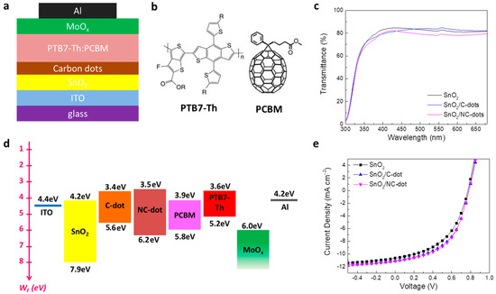
Figure 8.
(a) Schematic representation of the fabricated inverted OSCs. (b) Chemical structure of the donor and acceptor materials used in the photoactive blended layer. (c) Transmittance spectra of the SnO2 film coated with or without the C-dots and NC-dots. (d) Energy level diagram of the different layers used for the fabrication of the inverted OSCs. (e) Current density–voltage (J-V) characteristic curves measured under AM 1.5G illumination.
Figure 8d represents the energy level diagram of the materials used in the inverted OSCs. Note that, except the energy levels of the carbon nanodots, the work functions and energy levels of the SnO2, PTB7-Th and PCBM were taken from previous work [40,41]. As in the case of OLEDs, a reduction in the electron extraction barrier at the cathode/PCBM interface is observed, verifying the beneficial role of the nanodots coated atop the SnO2 film as cathode interlayers in the device performance. The current density–voltage (J-V) characteristic curves of the nanodot-based and reference OSCs are depicted in Figure 8e. A ~13% improvement in the device efficiency is observed for the OSCs with the nanodot interlayers, revealing the universality of the carbon dots used as ETLs in organic optoelectronic devices. In particular, the NC-dot-based device exhibited a short-circuit current density (JSC) of 11.14 mA cm−2, open-circuit voltage (VOC) of 0.78 V and fill factor (FF) of 0.52, resulting in a higher PCE of 4.52% compared with the reference cell, showing a PCE of 3.94% (JSC of 10.66 mA cm−2, VOC of 0.77 V and FF of 0.48). The device with the C-dots showed also higher electrical parameters (JSC of 11.08 mA cm−2, VOC of 0.78 V and FF of 0.51) and thus efficiency (PCE of 4.41%) with respect to the reference device.
4. Conclusions
We have demonstrated here the beneficial role of carbon nanodots with different surface functionalization in the performance of solution-processed green OLEDs and inverted OSCs. These materials were investigated for their optoelectronic properties and possible interaction with the organic semiconductors. Our experimental data indicate that they induce significant reductions in the electron injection/extraction barrier, therefore resulting in the fabrication of OLEDs and OSCs with significantly reduced turn-on voltages and increased short-circuit current density, respectively. Our results demonstrate the beneficial effects of abundant, carbon-based materials in organic optoelectronics for large-area applications.
Supplementary Materials
The following supporting information can be downloaded at: https://www.mdpi.com/article/10.3390/nano13010169/s1, Figure S1: Time-resolved photoluminescence (TRPL) spectra of F8BT, F8BT/C-dots, and F8BT/NC-dots; Figure S2: Water contact angle measurements taken in (a) F8BT, (b) F8BT/C-dots and (c) F8BT/NC-dots; Figure S3: (a) Absorption spectra and (b) tauc plots of pristine and nanodots-coated SnO2.
Author Contributions
Investigation, Z.G., A.V., K.L., K.M., G.C., K.-K.A. and E.K.E.; Writing-Original Draft, Z.G.; Methodology, L.C.P., E.K.E., S.G., A.R.b.M.Y. and K.A.; Formal Analysis, A.C.; Data Curation, A.C.; Conceptualization, A.G.C.; Writing-Review and editing, A.G.C., K.A. and A.S.; Supervision, M.V.; Project Administration, M.V.; Visualization, A.S. All authors have read and agreed to the published version of the manuscript.
Funding
This research was funded by the European Regional Development Fund of the European Union and Greek national funds through the Operational Program Competitiveness, Entrepreneurship and Innovation, under the call RESEARCH–CREATE–INNOVATE (project code:T2-EDK-04175-OLED-LUMIN-FOOD).
Data Availability Statement
The data that support the findings of this study can become available by the corresponding authors upon reasonable request.
Acknowledgments
This research has been co-financed by the European Regional Development Fund of the European Union and Greek national funds through the Operational Program Competitiveness, Entrepreneurship and Innovation, under the call RESEARCH–CREATE–INNOVATE (project code: T2-EDK-04175-OLED-LUMIN-FOOD).
Conflicts of Interest
The authors declare no conflict of interest.
References
- Tang, C.W.; VanSlyke, S.A. Organic Electroluminescent Diodes. Appl. Phys. Lett. 1987, 51, 913–915. [Google Scholar] [CrossRef]
- Steckl, A.J.; Heikenfeld, J.; Allen, S.C. Light Wave Coupled Flat Panel Displays and Solid-State Lighting Using Hybrid Inorganic/Organic Materials. J. Disp. Technol. 2005, 1, 157–166. [Google Scholar] [CrossRef]
- Davids, P.S.; Kogan, S.M.; Parker, I.D.; Smith, D.L. Charge Injection in Organic Light-emitting Diodes: Tunneling into Low Mobility Materials. Appl. Phys. Lett. 1996, 69, 2270–2272. [Google Scholar] [CrossRef]
- Ishii, H.; Sugiyama, K.; Ito, E.; Seki, K. Energy Level Alignment and Interfacial Electronic Structures at Organic/Metal and Organic/Organic Interfaces. Adv. Mater. 1999, 11, 605–625. [Google Scholar] [CrossRef]
- Yang, S.-M.; Jang, S.G.; Choi, D.-G.; Kim, S.; Yu, H.K. Nanomachining by Colloidal Lithography. Small 2006, 2, 458–475. [Google Scholar] [CrossRef] [PubMed]
- Khan, M.A.; Xu, W.; Wei, F.; Bai, Y.; Jiang, X.Y.; Zhang, Z.L.; Zhu, W.Q. Highly Efficient Organic Electroluminescent Diodes Realized by Efficient Charge Balance with Optimized Electron and Hole Transport Layers. Solid State Commun. 2007, 144, 343–346. [Google Scholar] [CrossRef]
- Patel, N.K.; Cina, S.; Burroughes, J.H. High-Efficiency Organic Light-Emitting Diodes. IEEE J. Sel. Top. Quantum Electron. 2002, 8, 346–361. [Google Scholar] [CrossRef]
- Qi, B.; Zhang, Z.G.; Wang, J. Uncovering the Role of Cathode Buffer Layer in Organic Solar Cells. Sci. Rep. 2015, 5, 7803. [Google Scholar] [CrossRef]
- Kadam, K.D.; Kim, H.; Rehman, S.; Patil, H.; Aziz, J.; Dongale, T.D.; Khan, M.F.; Kim, D.-K. Optimization of ZnO:PEIE as an Electron Transport Layer for Flexible Organic Solar Cells. Energy Fuels 2021, 35, 12416–12424. [Google Scholar] [CrossRef]
- Liu, C.; Xiao, C.; Li, W. Zinc Oxide Nanoparticles as Electron Transporting Interlayer inOrganic Solar Cells. J. Mater. Chem. C 2021, 9, 14093–14114. [Google Scholar] [CrossRef]
- Özgür, Ü.; Alivov, Y.I.; Liu, C.; Teke, A.; Reshchikov, M.A.; Doğan, S.; Avrutin, V.; Cho, S.-J.; Morkoç, H. A Comprehensive Review of ZnO Materials and Devices. J. Appl. Phys. 2005, 98, 041301. [Google Scholar] [CrossRef]
- Lee, H.; Park, I.; Kwak, J.; Yoon, D.Y.; Lee, C. Improvement of Electron Injection in Inverted Bottom-Emission Blue Phosphorescent Organic Light Emitting Diodes Using Zinc Oxide Nanoparticles. Appl. Phys. Lett. 2010, 96, 153306. [Google Scholar] [CrossRef]
- Huang, S.; Ali, N.; Huai, Z.; Ren, J.; Sun, Y.; Zhao, X.; Fu, G.; Kong, W.; Yang, S. A Facile Strategy for Enhanced Performance of Inverted Organic Solar Cells Based on Low-Temperature Solution-Processed SnO2 Electron Transport Layer. Org. Electron. 2020, 78, 105555. [Google Scholar] [CrossRef]
- Lee, H.; Kang, C.-M.; Park, M.; Kwak, J.; Lee, C. Improved Efficiency of Inverted Light-Emitting Diodes Using Tin Dioxide Nanoparticles as an Electron Injection Layer. ACS Appl. Mater. Interfaces 2013, 5, 1977–1981. [Google Scholar] [CrossRef]
- Li, Q.; Liu, H.; Sun, W.; Wang, S.; Dong, X.; Wang, L.; Li, X. Hole-Transporting Material Based on Spirobifluorene Unit with Perfect Amorphous and High Stability for Efficient OLEDs. J. Mater. Sci. Mater. Electron. 2019, 30, 11440–11450. [Google Scholar] [CrossRef]
- Ma, D.; Chen, Y. Organic Semiconductor Heterojunctions and Its Application in Organic Light-Emitting Diodes; Springer Series in Materials Science; Springer: Berlin/Heidelberg, Germany, 2017; Volume 250, ISBN 978-3-662-53693-3. [Google Scholar]
- Verykios, A.; Papadakis, M.; Soultati, A.; Skoulikidou, M.-C.; Papaioannou, G.; Gardelis, S.; Petsalakis, I.D.; Theodorakopoulos, G.; Petropoulos, V.; Palilis, L.C.; et al. Functionalized Zinc Porphyrins with Various Peripheral Groups for Interfacial Electron Injection Barrier Control in Organic Light Emitting Diodes. ACS Omega 2018, 3, 10008–10018. [Google Scholar] [CrossRef]
- Kalinowski, J. Organic Light-Emitting Diodes: Principles, Characteristics, and Processes; Optical Engineering; Marcel Dekker: New York, NY, USA, 2005; ISBN 978-0-8247-5947-6. [Google Scholar]
- Soultati, A.; Papadimitropoulos, G.; Davazoglou, D.; Argitis, P.; Alexandropoulos, D.; Politi, C.T.; Vainos, N.; Pistolis, G.; Coutsolelos, A.G.; Vasilopoulou, M. Near-IR Organic Light Emitting Diodes Based on Porphyrin Compounds. In Proceedings of the 2015 17th International Conference on Transparent Optical Networks (ICTON), Budapest, Hungary, 5–9 July 2015; pp. 1–4. [Google Scholar]
- Kido, J.; Ohtaki, C.; Hongawa, K.; Okuyama, K.; Nagai, K. 1,2,4-Triazole Derivative as an Electron Transport Layer in Organic Electroluminescent Devices. Jpn. J. Appl. Phys. 1993, 32, L917–L920. [Google Scholar] [CrossRef]
- Kido, J.; Hongawa, K.; Okuyama, K.; Nagai, K. Bright Blue Electroluminescence from Poly(N-vinylcarbazole). Appl. Phys. Lett. 1993, 63, 2627–2629. [Google Scholar] [CrossRef]
- Yu, G.; Yin, S.; Liu, Y.; Shuai, Z.; Zhu, D. Structures, Electronic States, and Electroluminescent Properties of a Zinc(II) 2-(2-Hydroxyphenyl)Benzothiazolate Complex. J. Am. Chem. Soc. 2003, 125, 14816–14824. [Google Scholar] [CrossRef]
- Kido, J.; Kimura, M.; Nagai, K. Multilayer White Light-Emitting Organic Electroluminescent Device. Science 1995, 267, 1332–1334. [Google Scholar] [CrossRef]
- Dailey, S.; Halim, M.; Rebourt, E.; Horsburgh, L.E.; Samuel, I.D.W.; Monkman, A.P. An Efficient Electron-Transporting Polymer for Light-Emitting Diodes. J. Phys. Condens. Matter 1998, 10, 5171–5178. [Google Scholar] [CrossRef]
- Yamamoto, T.; Maruyama, T.; Zhou, Z.-H.; Ito, T.; Fukuda, T.; Yoneda, Y.; Begum, F.; Ikeda, T.; Sasaki, S. Pi.-Conjugated Poly(Pyridine-2,5-Diyl), Poly(2,2’-Bipyridine-5,5’-Diyl), and Their Alkyl Derivatives. Preparation, Linear Structure, Function as a Ligand to Form Their Transition Metal Complexes, Catalytic Reactions, n-Type Electrically Conducting Properties, Optical Properties, and Alignment on Substrates. J. Am. Chem. Soc. 1994, 116, 4832–4845. [Google Scholar] [CrossRef]
- Vasilopoulou, M.; Douvas, A.M.; Georgiadou, D.G.; Palilis, L.C.; Kennou, S.; Sygellou, L.; Soultati, A.; Kostis, I.; Papadimitropoulos, G.; Argitis, P. The Influence of Hydrogeneration and Oxygen Vacancies on Molybdenum Oxides Work Function and Gap States for Application in Organic Optoelectronics. J. Am. Chem. Soc. 2012, 134, 16178–16187. [Google Scholar] [CrossRef] [PubMed]
- Pal, A.; Natu, G.; Ahmad, K.; Chattopadhyaya, A. Phosphorus Induced Crystallinity in Carbon Dots for Solar Light Assisted Seawater Desalination. J. Mater. Chem. A 2018, 6, 4111–4118. [Google Scholar] [CrossRef]
- Lee, B.R.; Lee, S.; Park, J.H.; Jung, E.D.; Yu, J.C.; Nam, Y.S.; Heo, J.; Kim, J.-Y.; Kim, B.-S.; Song, M.H. Amine-Based Interfacial Molecules for Inverted Polymer-Based Optoelectronic Devices. Adv. Mater. 2015, 27, 3553–3559. [Google Scholar] [CrossRef]
- Omer, K.M.; Tofiq, D.I.; Hassan, A.Q. Solvothermal Synthesis of Phosphorus and Nitrogen Doped Carbon Quantum Dots as a Fluorescent Probe for Iron(III). Microchim. Acta 2018, 185, 466. [Google Scholar] [CrossRef]
- Zhang, H.; Chen, Y.; Liang, M.; Xu, L.; Qi, S.; Chen, H.; Chen, X. Solid-Phase Synthesis of Highly Fluorescent Nitrogen-Doped Carbon Dots for Sensitive and Selective Probing Ferric Ions in Living Cells. Anal. Chem. 2014, 86, 9846–9852. [Google Scholar] [CrossRef]
- de Amorim Lima, N.; Camargo Avila, H.; do Nascimento Marchiori, C.; Gondim Sampaio, S.; Ferreira Mota, J.; Gomes Pereira Ribeiro, V.; da Silva Clemente, C.; Mele, G.; Cremona, M.; Mazzetto, S. Light-Emitting Porphyrin Derivative Obtained from a Subproduct of the Cashew Nut Shell Liquid: A Promising Material for OLED Applications. Materials 2019, 12, 1063. [Google Scholar] [CrossRef]
- Sultan Erkan Theoretical and Experimental Spectroscopic Properties and Molecular Docking of F8BT P-Type Semiconducting Polymer. Russ. J. Phys. Chem. A 2020, 94, 445–452. [CrossRef]
- Ayesta, I.; Illarramendi, M.A.; Arrue, J.; Jimenez, F.; Zubia, J.; Bikandi, I.; Ugartemendia, J.M.; Sarasua, J.-R. Luminescence Study of Polymer Optical Fibers Doped With Conjugated Polymers. J. Light. Technol. 2012, 30, 3367–3375. [Google Scholar] [CrossRef]
- Jeong, K.W.; Kim, H.S.; Yi, G.R.; Kim, C.K. Enhancing the Electroluminescence of OLEDs by Using ZnO Nanoparticle Electron Transport Layers That Exhibit the Auger Electron Effect. Mol. Cryst. Liq. Cryst. 2018, 663, 61–70. [Google Scholar] [CrossRef]
- Li, W.; Wu, X.; Liu, G.; Li, Y.; Wu, L.; Fu, B.; Wang, W.; Zhang, D.; Zhao, J. Enhanced Electron Transportation of PF-NR2 Cathode Interface by Gold Nanoparticles. Nanoscale Res. Lett. 2019, 14, 261. [Google Scholar] [CrossRef] [PubMed]
- Sun, H.; Chen, Y.; Zhu, L.; Guo, Q.; Yang, D.; Chen, J.; Ma, D. Realization of Optimal Interconnector for Tandem Organic Light-Emitting Diodes with Record Efficiency. Adv. Electron. Mater. 2015, 1, 1500176. [Google Scholar] [CrossRef]
- Sardar, G.; Shukla, A.; Moore, E.G.; Banappanavar, G.; Lo, S.-C.; Namdas, E.B.; Kabra, D. Reduced Singlet-Triplet Annihilation for Low Threshold Aplified Spontaneous Emission from a Blue Polyfluorene Electroluminescent Organic Semiconductor. J. Phys. Chem. C 2022, 126, 9069–9075. [Google Scholar] [CrossRef]
- Morii, K.; Fukagawa, H. Hybrid Organic-Inorganic Light-Emitting Diode. In Air-Stable Inverted Organic Light-Emitting Diodes; SpringerBriefs in Applied Sciences and Technology; Springer: Cham, Switzerland, 2020. [Google Scholar] [CrossRef]
- Giebink, N.C.; Wiederrecht, G.P.; Wasielewski, M.R.; Forrest, S.R. Ideal Diode Equation for Organic Heterojunctions. I. Derivation and Application. Phys. Rev. B 2010, 82, 155305. [Google Scholar] [CrossRef]
- Soultati, A.; Verykios, A.; Panagiotakis, S.; Armadorou, K.-K.; Haider, M.I.; Kaltzoglou, A.; Drivas, C.; Fakharuddin, A.; Bao, X.; Yang, C.; et al. Suppressing the Photocatalytic Activity of Zinc Oxide Electron-Transport Layer in Nonfullerene Organic Solar Cells with a Pyrene-Bodipy Interlayer. ACS Appl. Mater. Interfaces 2020, 12, 21961–21973. [Google Scholar] [CrossRef] [PubMed]
- Guo, F.; Sun, X.; Ynag, Z.; Wei, J.; Xu, D. Enhanced Lifetime and Photostability with Low-Temperature Mesoporous ZnTiO3/Compact SnO2 Electrodes in Perovskite Solar Cells. Angew. Chem. 2019, 58, 18460–18465. [Google Scholar] [CrossRef]


Disclaimer/Publisher’s Note: The statements, opinions and data contained in all publications are solely those of the individual author(s) and contributor(s) and not of MDPI and/or the editor(s). MDPI and/or the editor(s) disclaim responsibility for any injury to people or property resulting from any ideas, methods, instructions or products referred to in the content. |
© 2022 by the authors. Licensee MDPI, Basel, Switzerland. This article is an open access article distributed under the terms and conditions of the Creative Commons Attribution (CC BY) license (https://creativecommons.org/licenses/by/4.0/).