Abstract
A switchable and tunable terahertz (THz) metamaterial based on photosensitive silicon and Vanadium dioxide (VO2) was proposed. By using a finite-difference time-domain (FDTD) method, the transmission and reflective properties of the metamaterial were investigated theoretically. The results imply that the metamaterial can realize a dual electromagnetically induced transparency (EIT) or two narrow-band absorptions depending on the temperature of the VO2. Additionally, the magnitude of the EIT and two narrow-band absorptions can be tuned by varying the conductivity of photosensitive silicon (PSi) via pumping light. Correspondingly, the slow-light effect accompanying the EIT can also be adjusted.
1. Introduction
Terahertz waves are electromagnetic waves with frequencies in the range of 0.1 THz to 100 THz and wavelengths in the range of 3 μm to 3 mm, between microwave and infrared. THz technology has great potential for applications in sensing, communication, and imaging [1,2,3]. However, its development has been hampered by the limitations of natural materials. In recent years, with the advanced development of micro- and nanoprocessing technology [4,5,6], metamaterials with complex structures and increasingly small dimensions are also contributing to the rapid development of THz technology. Using metamaterials [7], researchers have designed various efficient optical micro–nano devices such as absorbers [8,9,10], polarization converters [11,12], and electromagnetically induced transparency (EIT) devices [13,14,15]. The EIT effect results from its high transmission peaks in the low-transmission region. Large dispersion and group delay effects occur near the peak frequency of the EIT transmission peak. The effect has very promising applications in the field of slow light, promotes the enhancement of optical non-linear effects, and has an equally positive effect on the development of all-optical information devices such as optical caches, optical switches, and optical routers [16,17,18,19]. The absorption effect in terahertz metamaterials has promising applications in areas such as filters, stealth devices, and highly sensitive sensors [9,20]. However, conventional THz metamaterials cannot change their properties after they are fabricated and have a single function, which leads to high practical costs, which means tunable and switchable multifunctional terahertz metamaterials are necessary.
At present, the tuning of THz metamaterials is mainly based on active materials such as VO2, PSi, etc. [21]. VO2 is a transition-metal oxide with the property of reversible phase transition. The phase transition temperature is about 340 K, which makes the phase transition of VO2 easy to control [21,22,23,24]. PSi is a semiconductor whose conductivity can be changed easily by tuning the intensity of light on it [25]. In 2012, J. Gu et al. combined photoconductive silicon substrates with planar metamaterial units to achieve a THz EIT effect with photocontrolled configurability [26]. In 2016, Zhang et al. proposed a dynamically modulated THz absorber combining VO2 films with arrays of structured copper rings. The absorber achieved a modulation depth of approximately 78% under light induction [27]. In 2018, Liu et al. introduced a dynamically tunable THz metamaterial consisting of graphene and two cut-line metal resonance rings. They realized an EIT effect with an 81% modulation depth and an actively controlled slow-light effect [28]. In 2020, Zheng et al. designed a tunable EIT terahertz metamaterial consisting of two Au split-disk resonant rings on top and bottom, with a modulation depth of 75.58% [29]. As can be seen, the studies above concerning THz metamaterials focused mainly on single functions, and had lower modulation depths. In fact, it is necessary to develop new THz metamaterials with tunable multifunctions and high modulation depths.
In this paper, we design a switchable THz metamaterial with a tunable EIT effect and absorption based on PSi and VO2. The metamaterial consists of metal bars and two square resonant rings of different sizes forming a metal layer, a dielectric layer, and a VO2 film. The properties of the designed metamaterial are investigated theoretically by means of the FDTD method. It is found that when the temperature of VO2 is set to be room temperature it is in the dielectric state, and the metamaterial exhibits a double EIT effect and can achieve a double slow-light effect. When the temperatures are above the phase transition temperature, VO2 is in a metal state and the metamaterial shows a double narrow-band absorption. When the conductivity of the PSi changes, the magnitude of EIT and absorption can be changed and both have a high modulation depth. The structure designed in this paper can be used in devices such as bio-detectors, sensors, optical switches, etc., in the corresponding frequency range [30].
2. Materials and Methods
The designed metamaterial is arranged in a periodic pattern unit with P = 200 μm. As shown in Figure 1a, from top to bottom, the unit consists of four layers which are metal layer, dielectric layer (SiO2), VO2 film, and dielectric layer (SiO2). Correspondingly, the thickness of each layer is h1 = 3 μm, h2 = 25 μm, h3 = 0.2 μm, and h4 = 14.8 μm, respectively. As shown in Figure 1b, the metal layer consists of metal bar (MB), large resonant ring (LRR), and small resonant ring (SRR). The length of MB is L = 160 μm, and both SRR and LRR are square rings with side lengths of a = 30 μm and b = 35 μm, respectively. The width of MB and ring is k = 5 μm. Each ring has a gap filled with g = 5 μm PSi. The distribution of each structure is given by S1 = 47.5 μm, S2 = 5 μm, and S3 = 37.5 μm.
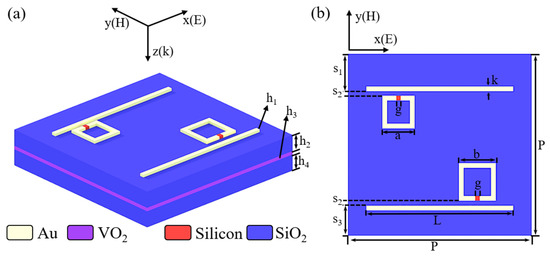
Figure 1.
(a) Unit structure; (b) top view of unit structure.
The properties of the metamaterial were investigated using FDTD. When conducting simulation, the THz plane wave propagates in the Z-axis direction and its polarization is in the X-axis direction. In THz band, gold is considered to be a lossy metal, and its conductivity can be obtained as 4.56 × 10⁷ S/m via a static model [31]. The relative dielectric constants of SiO2 and PSi are 2.9 and 11.9, respectively [32].
The optical properties of VO2 are illustrated using the Drude model [33,34,35,36,37]:
where is the dielectric constant of VO2 at infinite frequency, and rad/s is collision frequency [35]. The plasma frequency can be characterized as , where rad/s, S/m [36]. The conductivity of VO2 is 1 S/m or 2 × 10⁵ S/m when it is insulating or in metal phase.
Figure 2 shows the change in conductivity of VO2 with temperature, which was controlled by using electrical heating and a semiconductor refrigeration sheet. Heating from absorbed radiation will have a certain effect on the absorption characteristics of the absorber, but it is weak and can be neglected [38]. And the physical properties of Au, SiO2, and PSi remain essentially unchanged over the temperature range of the VO2 phase transition [38,39].
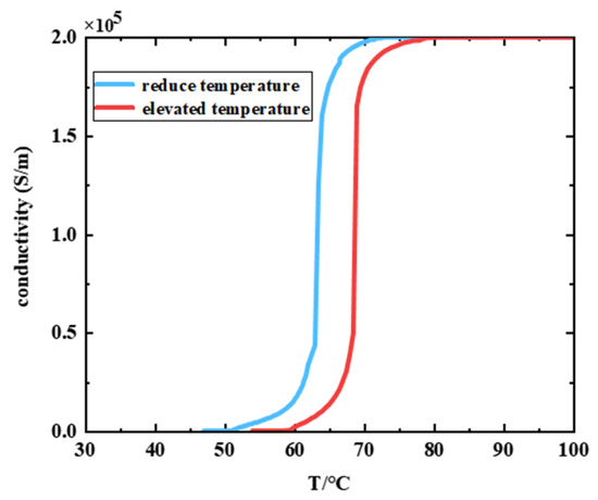
Figure 2.
Conductivity of VO2 as a function of temperature.
The conductivity of the PSi can be controlled by light and expressed as follows [40]:
where I is the intensity of the pump light. The conductivity of the PSi is 1 S/m and 1 × 10⁵ S/m when the intensity of the pump light is 0 or 249 μJ/cm2, respectively [25]. VO2 can also be excited by pump light, but its excitation intensity is 8 mJ/cm2, which is much greater than the excitation intensity of PSi [41], so the excitation of PSi with the pump light has almost no effect on VO2.
3. Results and Discussion
3.1. Electromagnetically Induced Transparency
Firstly, we studied theoretically the transmission properties of the metamaterial when VO2 is below the phase-change temperature and the pumping light of the PSi is off. In this case, the conductivity of VO2 (25 °C) and PSi is 1 S/m [42], and the results are shown in Figure 3a. We can see that there are two transmission peaks at 0.73 THz and 0.862 THz, defined as PEAK 1 and PEAK 2, respectively. In order to investigate the origin of the transmission peaks, we individually calculated the transmissions of the MB array, the SRR array, and the LRR array, which are shown in Figure 3b using black, red, and blue solid lines, respectively. Specifically, the MB array shows a broadband valley around the frequency of 0.723 THz, which is usually believed to result from Lorentzian resonance caused by incident light [32]. However, the SRR and LRR arrays produce two ultra-narrow transmission valleys at 0.909 THz and 0.778 THz, respectively, which is usually believed to result from LC resonance caused by incident light [26]. The transmittance peaks 1 and 2 arise from the coupling of the narrowband mode and broadband mode, in which the broadband mode is referred to as bright mode and the narrowband mode as dark mode [43]. The bright and dark modes produce destructive interference at specific frequencies due to their different bandwidths, leading to the EIT effect [14].
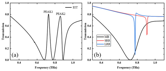
Figure 3.
(a) Transmission spectra of structures consisting of MBs, SRRs, and LRRs at a conductivity of 1 S/m for both PSi and VO2, (b) transmission spectra of structures of MB, SRR, and LRR.
To further explain the formation of the two EIT transmission peaks, as shown in Figure 4a,b, we provided the electric field distribution at 0.73 THz and 0.862 THz, respectively. The EIT effect transmission peak 1 at 0.73 THz is generated from the coupling of the LRR and the MB, while the EIT transmission peak 2 at 0.862 THz results from the coupling of the SRR ring and the MB [32]. The two different couplings produce two EIT transmission peaks in the transmission spectrum, achieving a double-channel effect.
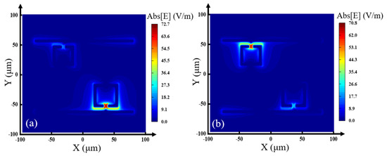
Figure 4.
Electric field distribution of the EIT transmission peak at (a) 0.73 THz, (b) 0.862 THz.
Secondly, we studied the transmission properties and slow-light effect of the metamaterial when the temperature of VO2 is below the phase-change temperature and the pumping light of the PSi is on. In this case, the conductivity of VO2 is still 1 S/m and the conductivity of PSi increases from 1 S/m to 240 S/m. The transmission characteristics of the metamaterial are shown in Figure 5a, where we can see that the peak transmittances at 0.73 THz and 0.862 THz are 0.804 and 0.769, respectively, at 1 S/m for PSi. As the conductivity of the PSi increases, the amplitudes of peaks 1 and 2 begin to decrease and the peak frequency at peak 2 begins to redshift. When the conductivity of the PSi reaches 240 S/m, the peak transmittance values at frequencies of 0.73 THz and 0.862 THz are 0.08 and 0.31, respectively, and the transmittance spectral curve becomes an approximate Lorentz curve. The decrease in the transmission is due to the modulation of the dark mode by the increased conductivity of PSi. The PSi is located at the SRR and LRR notch, and an increase in its conductivity causes a decrease in the resonant strength of the SRR and LRR, affecting the coupling of the SRR and LRR with the CW, which in turn affects the amplitude and frequency position of peaks 1 and 2 [26]. The modulation depth of the transmission peak can be expressed as follows [14]:
where T0 and T1 are the transmittance of the PSi conductivity at 1 S/m and 240 S/m, respectively. T0 and T1 at 0.73 THz were 0.804 and 0.08, respectively, and T0 and T1 at 0.862 THz were 0.769 and 0.31, respectively. Using Equation (3), we can solve for modulation depths of 90.05% and 59.69% at 0.73 THz and 0.862 THz, respectively.
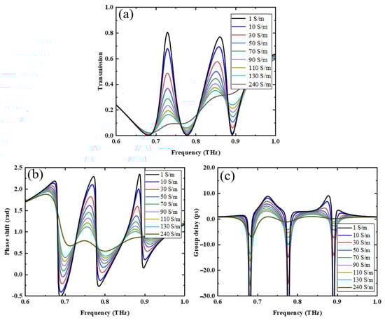
Figure 5.
(a) Transmission spectrum, (b) phase-shift spectrum, (c) group delay variation in PSi at different conductivities for a VO2 conductivity of 1 S/m.
The slow-light effect is an important application of EIT and is often described by the group delay:
where is the phase shift of EIT and is the angular frequency of EIT [14]. Figure 5b,c show the phase shift and group delay of the EIT effect for different conductivities of PSi in Figure 5a. When the conductivity of PSi is 1 S/m, the phase shift shows steep jumps near the two transmission peaks and achieves group delays of 8.79 ps and 9.04 ps, corresponding to free-space propagation distances of 2.64 mm and 2.71 mm. This means that by controlling the conductivity of the photosensitive silicon, the optical path difference can be varied. The effect can be used in practical applications such as quantum communications and slow optical devices [30]. As the conductivity increases, the phase shift decreases, and group delay gradually diminishes. When the conductivity of the PSi reaches 240 S/m, the phase shift jumps, the group delay properties almost disappear, and the slow-light effect caused by the MB gradually becomes apparent. Thus, the regulation of the double slow-light effect can be achieved by changing the conductivity of the PSi.
Then, at different conductivities of photosensitive silicon, the theoretical fitting of the EIT transmission spectrum is carried out using the two-resonator model expressed by specific equations which are as follows [44]:
where x1 and x2 are the displacement, and E is the incident electric field. (w1, w2) and (, ) are the resonant angular frequencies and loss factors of the bright and dark modes, respectively, denotes the coupling strength between the bright and dark modes, and (Q, q) and (M, m) denote the effective charge and effective mass, respectively. The dimensionless constants, A and B, are defined using A = Q/q and B = M/m to describe the relative coupling of the incident light to the bright and dark modes. The linear polarization rate χ can be obtained with Equation (5) and the transmission coefficient T can be derived from theoretical analysis. Figure 6a–c show the theoretical and simulated curves of the EIT transmission spectra using the coupled resonator model when the conductivities of PSi are 1 S/m, 70 S/m, and 240 S/m, respectively. From the figure, it can be seen that the theoretical fitted curves match well with the simulated curves in the EIT functional mode.
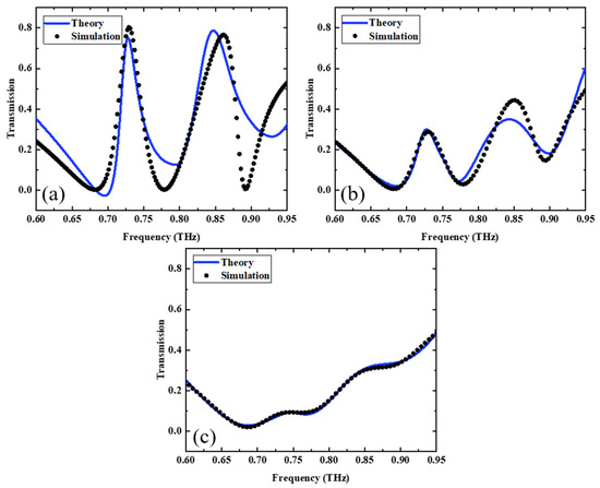
Figure 6.
Simulated and theoretical fitted transmission spectra of LRR coupled to MB at photosensitive silicon conductivities of (a) 1 S/m, (b) 70 S/m, (c) 240 S/m.
Finally, we studied the size effect of the metamaterial when VO2 is below the phase-change temperature and the pumping power of the photosensitive silicon is off. In this case, the conductivity of VO2 and photosensitive silicon is 1 S/m, and the results are shown in Figure 7. Figure 7a shows the transmission spectrum for a constant LRR size of 35 μm and SRR sizes of 25 μm, 30 μm, and 35 μm, respectively. As the size of the SRR increases, a redshift occurs in the transmission peak and the two transmission valleys on the right side. Figure 7b shows the transmission spectrum for a constant SRR size of 30 μm and for LRR sizes of 30 μm, 35 μm, and 40 μm, respectively. As the LRR size increases, a redshift occurs in the left transmission peak and the two transmission valleys. The peak transmission on the left side is related to the size of the LRR, while the peak transmission on the right side is related to the size of the SRR. Figure 7c shows the transmission spectra of the SRR at 5 μm, 10 μm, and 15 μm distances from the MB when the LRR is at a constant distance of 5 μm from the MB. As the distance increases, the transmission peak and two transmission valleys on the right show a blueshift. Figure 7d shows the transmission spectra of the LRR with MB distances of 5 μm, 10 μm, and 15 μm when the SRR is at a constant distance of 5 μm from the MB. As the distance increases, the transmission peak and two transmission valleys on the left experience a blueshift. It is further shown that the transmission peak on the left side is related to the LRR and the transmission peak on the right side is related to the SRR. In summary, the dual-channel effect is generated by the coupling of two resonant rings to metal bars.
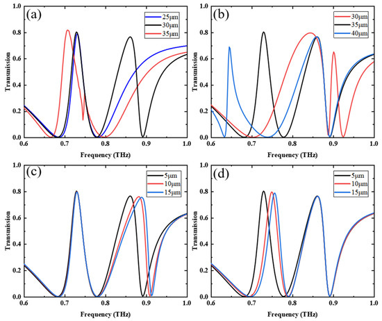
Figure 7.
(a) Transmission spectrum when LRR size is constant and SRR size is varied, (b) transmission spectrum when the SRR size is constant and the LRR size is varied; EIT effect transmission spectra at different (c) SRR, (d) LRR, and CW distances.
3.2. Absorption
When the pumping power of the PSi is off, its conductivity is 1 S/m. When VO2 is above the phase-change temperature (87 °C) [42], its conductivity is 2 × 10⁵ S/m, and it is in its metal state. In this case, we studied the absorption properties of the metamaterial. Absorbance can be calculated using A = 1 − R − T = 1 − − , where R stands for reflectance and T for transmittance, and the and are the reflection and transmission coefficients obtained from the S-parameters [45]. The thickness of VO2 film is 200 nm and larger than the terahertz crust depth, which makes terahertz almost impermeable [9], so T = 0, A = 1 − R = 1 − . The reflection spectrum was calculated using FDTD, and correspondingly the absorption spectrum was obtained and is shown in Figure 8a, where two absorption peaks are at 0.752 THz and 0.885 THz, respectively.
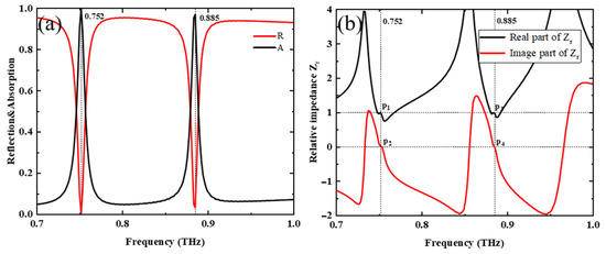
Figure 8.
(a) Absorption and reflection spectra of metamaterials with PSi conductivity of 1 S/m and VO2 conductivity of 2 × 10⁵ S/m, (b) schematic diagram of the real and imaginary parts of impedance matching.
We studied the origin of the absorption peaks using impedance-matching theory, shown as follows [46,47,48]:
where Z is the effective impedance, Z0 is the free-space impedance, and the relative impedance is expressed as . When , the absorption rate is 1 and the impedance of the metamaterial matches that of the free space. Figure 8b shows the corresponding impedance plots, where the real part and imaginary part of the relative impedance are shown with black and red lines, respectively. At p1 and p2, the real and imaginary values of the relative impedance are 1 and 0, respectively, which means impedance matching occurs here. The same effect happens at p3 and p4, and p1, p2, p3, and p4 present evidence of perfect absorption at 0.752 THz and 0.885 THz, respectively.
To further explain the formation of the two absorption peaks, we calculated the electric field distribution of the structure at frequencies of 0.752 THz and 0.885 THz, which are shown in Figure 9a and Figure 9b, respectively. From Figure 9a, we can find that the electric field enhancement is mainly distributed in the gap between the LRR and the MB, which means the absorption peak at 0.752 THz mainly originates from the coupling of the LRR to the MB. From Figure 9b, we can see that the electric field enhancement is mainly distributed in the gap between the SRR and the MB, which means the absorption peak at 0.885 THz mainly originates from the coupling of the SRR to the MB. The two different coupling modes produce a double narrow-band absorption peak in the absorption spectrum.
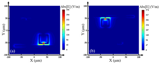
Figure 9.
Electric field distribution of the absorption peak at (a) 0.752 THz and (b) 0.885 THz.
In addition, we studied the absorption properties of the metamaterial when VO2 is above the phase-change temperature and the pumping power of the PSi is on. In this case, the conductivity of VO2 is 2 × 10⁵ S/m and the conductivity of PSi is adjusted from 1 S/m to 105 S/m by changing the intensities of the pump light. Figure 10a shows the change in absorption with the conductivity of PSi. When the conductivity is 1 S/m, the absorption peak is the highest. As the conductivity increases, the absorption peak decreases gradually. When the conductivity is 105 S/m, the absorption peak disappears, which means that the resonance between LRR and SRR and MB disappears. The above simulation results were then analyzed quantitatively using impedance-matching theory. The real and imaginary parts of the relative impedance Zr were calculated using the MATLAB program for different PSi conductivities, and the results are shown in Figure 10b,c. As shown in Figure 10b, as the PSi conductivity increases, the real part of the relative impedance Zr at the peak absorption frequency gradually deviates from 1. Similarly, in Figure 10c, as the PSi conductivity increases, the imaginary part of the relative impedance Zr at the peak absorption frequency gradually deviates from 0. These theoretical data validate the simulation results in Figure 10a, where the absorption peak decreases as the PSi conductivity increases.
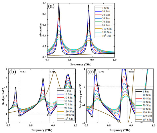
Figure 10.
(a) Absorption spectra of PSi at different conductivities when the conductivity of VO2 is 2 × 10⁵ S/m; (b) real and (c) imaginary parts of relative Zr for PSi at different conductivities when the conductivity of VO2 is 2 × 10⁵ S/m.
In fact, at peak frequency, the conductivity of the PSi located at the SRR and LRR notches affects the impedance match between the metamaterial and the free space. High conductivity causes weak matching and low absorption [9]. Specifically, when the conductivity of PSi was 1 S/m or 105 S/m, the amplitudes of absorption at 0.752 THz and 0.885 THz were 0.998 and 0.97 or 0.036 and 0.055, respectively. So, the modulation depths of the structure can be obtained via Equation (3) to be 96.39% and 94.33% at 0.752 THz and 0.885 THz frequencies, respectively.
Finally, we studied the size effect of the metamaterial when VO2 is above the phase-change temperature and the pumping power of the photosensitive silicon is off. In this case, the conductivity of VO2 is 2 × 10⁵ S/m and photosensitive silicon is 1 S/m, and the results are shown in Figure 11. Figure 11a shows the absorption spectra for a constant LRR size of 35 μm and SRR sizes of 25 μm, 30 μm, and 35 μm, respectively. As the SRR size increases, the absorption peak on the right side shows a redshift. Figure 11b shows the absorption spectra of a constant SRR size of 30 μm and 35 μm, 40 μm, and 45 μm LRR sizes, respectively. As the LRR size increases, the absorption peak on the left shows a redshift. Therefore, the absorption peak on the left side is related to the size of the LRR, while the absorption peak on the right side is related to the size of the SRR. Figure 11c shows the absorption spectra of the SRR at 5 μm, 10 μm, and 15 μm from MB when the LRR is kept at a constant distance of 5 μm from the MB. As the distance increases, the absorption peak on the right side shows a blueshift. Figure 11d shows the absorption spectra of the LRR at 5 μm, 10 μm, and 15 μm from the MB when the SRR is kept at a constant distance of 5 μm from the MB. As the distance increases, the absorption peak on the left shows a blueshift. In summary, the double absorption peak is generated by the coupling of the two resonant rings to the metal bar.
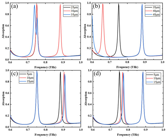
Figure 11.
(a) Absorption spectrum when LRR size is constant and SRR size varies; (b) absorption spectrum when SRR size is constant and LRR size varies; absorption spectra at different (c) SRR, (d) LRR, and CW distances.
For comparison, in Table 1 we list some related work. From the table, we found that the proposed structure has a higher modulation depth for the EIT effect. Moreover, it also has a higher absorption modulation depth.

Table 1.
Comparison of designed metamaterials with reported metamaterials.
4. Conclusions
In summary, we have designed a dual-function switchable and tunable THz metamaterial by using VO2 and PSi. When VO2 was in the dielectric state, the THz metamaterial produced a double EIT effect at frequencies of 0.73 THz and 0.862 THz and achieved group delays of 8.79 ps and 9.04 ps. And varying the conductivity of PSi could tune the amplitude of the transmission peak and group delay. When VO2 was in the metallic state, the metamaterial produced two perfect absorption peaks at 0.752 THz and 0.885 THz. And the amplitude of the absorption peak could be tuned by varying the conductivity of PSi. The modulation depths of the two absorption peaks could reach 96.39% and 94.33%, respectively. Compared to previous designs, we have achieved a dual-function integration that breaks the limitations of a single function and achieves a higher modulation depth per function, which will provide devices like optical modulators, optical switchers, and photodetectors with higher sensitivity.
Author Contributions
Conceptualization, X.Z. and Y.G.; methodology, X.Z. and Y.G.; software, X.Z. and Y.G.; validation, X.Z., G.W. and Y.G.; formal analysis, X.Z. and J.L.; investigation, X.Z., S.Z., M.L., S.Y., Y.J. and Y.G.; writing—original draft preparation, X.Z.; writing—review and editing, X.Z. and Y.G.; funding acquisition, Y.G. All authors have read and agreed to the published version of the manuscript.
Funding
Natural Science Foundation of Heilongjiang Province (LH2020F041); Fundamental Research Funds in Heilongjiang Provincial Universities (145209148).
Data Availability Statement
All content and data are displayed in the manuscript.
Conflicts of Interest
The authors declare no conflict of interest.
References
- Otter, W.J.; Lucyszyn, S. Hybrid 3-D-Printing Technology for Tunable THz Applications. Proc. IEEE 2017, 105, 756–767. [Google Scholar] [CrossRef]
- Wang, J.; Tian, H.; Wang, Y.; Li, X.Y.; Cao, Y.J.; Li, L.; Liu, J.L.; Zhou, Z.X. Liquid crystal terahertz modulator with plasmon-induced transparency metamaterial. Opt. Express 2018, 26, 5769–5776. [Google Scholar] [CrossRef] [PubMed]
- Zhang, M.J.; Hong, H.C.; Lin, H.J.; Shen, L.G.; Yu, H.Y.; Ma, G.C.; Chen, J.R.; Liao, B.Q. Mechanistic insights into alginate fouling caused by calcium ions based on terahertz time-domain spectra analyses and DFT calculations. Water Res. 2018, 129, 337–346. [Google Scholar] [CrossRef] [PubMed]
- Fang, N.; Lee, H.; Sun, C.; Zhang, X. Sub-diffraction-limited optical imaging with a silver superlens. Science 2005, 308, 534–537. [Google Scholar] [CrossRef]
- Schurig, D.; Mock, J.J.; Justice, B.J.; Cummer, S.A.; Pendry, J.B.; Starr, A.F.; Smith, D.R. Metamaterial electromagnetic cloak at microwave frequencies. Science 2006, 314, 977–980. [Google Scholar] [CrossRef]
- Zheludev, N.I. The Road Ahead for Metamaterials. Science 2010, 328, 582–583. [Google Scholar] [CrossRef]
- Iyer, A.; Kremer, P.; Eleftheriades, G. Experimental and theoretical verification of focusing in a large, periodically loaded transmission line negative refractive index metamaterial. Opt. Express 2003, 11, 696–708. [Google Scholar] [CrossRef]
- Barzegar-Parizi, S.; Ebrahimi, A. Ultrathin, polarization-insensitive multi-band absorbers based on graphene metasurface with THz sensing application. J. Opt. Soc. Am. B Opt. Phys. 2020, 37, 2372–2381. [Google Scholar] [CrossRef]
- Wang, G.; Wu, T.; Jia, Y.; Gao, Y.; Gao, Y.C. Switchable Terahertz Absorber from Single Broadband to Dual Broadband Based on Graphene and Vanadium Dioxide. Nanomaterials 2022, 12, 2172. [Google Scholar] [CrossRef]
- Tao, H.; Landy, N.I.; Bingham, C.M.; Zhang, X.; Averitt, R.D.; Padilla, W.J. A metamaterial absorber for the terahertz regime: Design, fabrication and characterization. Opt. Express 2008, 16, 7181–7188. [Google Scholar] [CrossRef]
- Li, J.S.; Li, X.J. Switchable tri-function terahertz metasurface based on polarization vanadium dioxide and photosensitive silicon. Opt. Express 2022, 30, 12823–12834. [Google Scholar] [CrossRef] [PubMed]
- Liao, S.Y.; Sui, J.Y.; Zhang, H.F. Switchable ultra-broadband absorption and polarization conversion metastructure controlled by light. Opt. Express 2022, 30, 34172–34187. [Google Scholar] [CrossRef] [PubMed]
- Liu, N.; Langguth, L.; Weiss, T.; Kastel, J.; Fleischhauer, M.; Pfau, T.; Giessen, H. Plasmonic analogue of electromagnetically induced transparency at the Drude damping limit. Nat. Mater. 2009, 8, 758–762. [Google Scholar] [CrossRef] [PubMed]
- Wu, T.; Shao, Y.B.; Buyingaridi; Ma, S.; Gao, Y.C. Terahertz hybrid metal-graphene metamaterials with tunable dual-band electromagnetically induced transparency. Optik 2021, 240, 166784. [Google Scholar] [CrossRef]
- Wang, T.L.; Li, T.T.; Yao, H.Y.; Lu, Y.Y.; Yan, X.; Cao, M.Y.; Liang, L.J.; Yang, M.S.; Yao, J.Q. High-sensitivity modulation of electromagnetically induced transparency analog in a THz asymmetric metasurface integrating perovskite and graphene. Photonics Res. 2022, 10, 2317–2327. [Google Scholar] [CrossRef]
- Chen, H.; Zhang, H.Y.; Liu, M.D.; Zhao, Y.K.; Liu, S.D.; Zhang, Y.P. Tunable multiple plasmon-induced transparency in three-dimensional Dirac semimetal metamaterials. Opt. Commun. 2018, 423, 57–62. [Google Scholar] [CrossRef]
- Jiang, Y.; Ning, H.Y.; Tian, C.G.; Jiang, B.J.; Li, Q.; Yan, H.J.; Zhang, X.L.; Wang, J.Q.; Jing, L.Q.; Fu, H.G. Single-crystal TiO2 nanorods assembly for efficient and stable cocatalyst-free photocatalytic hydrogen evolution. Appl. Catal. B Environ. 2018, 229, 1–7. [Google Scholar] [CrossRef]
- Zhao, J.X.; Song, J.L.; Zhou, Y.; Zhao, R.L.; Zhou, J.H. Tunable multiple plasmon-induced transparency in a simple terahertz Dirac semimetal based metamaterial. Opt. Mater. Express 2019, 9, 3325–3332. [Google Scholar] [CrossRef]
- Wu, T.; Wang, G.; Jia, Y.; Shao, Y.B.; Gao, Y.; Gao, Y.C. Multi-control plasmon-induced transparency via graphene and bulk Dirac semimetal. Diam. Relat. Mater. 2022, 129, 109369. [Google Scholar] [CrossRef]
- Alves, F.; Kearney, B.; Grbovic, D.; Karunasiri, G. Narrowband terahertz emitters using metamaterial films. Opt. Express 2012, 20, 21025–21032. [Google Scholar] [CrossRef]
- Jeong, Y.G.; Han, S.; Rhie, J.; Kyoung, J.S.; Choi, J.W.; Park, N.; Hong, S.; Kim, B.J.; Kim, H.T.; Kim, D.S. A Vanadium Dioxide Metamaterial Disengaged from Insulator-toMetal Transition. Nano Lett. 2015, 15, 6318–6323. [Google Scholar] [CrossRef] [PubMed]
- Dicken, M.J.; Aydin, K.; Pryce, I.M.; Sweatlock, L.A.; Boyd, E.M.; Walavalkar, S.; Ma, J.; Atwater, H.A. Frequency tunable near-infrared metamaterials based on VO2 phase transition. Opt. Express 2009, 17, 18330–18339. [Google Scholar] [CrossRef]
- Kats, M.A.; Sharma, D.; Lin, J.; Genevet, P.; Blanchard, R.; Yang, Z.; Qazilbash, M.M.; Basov, D.N.; Ramanathan, S.; Capasso, F. Ultra-thin perfect absorber employing a tunable phase change material. Appl. Phys. Lett. 2012, 101, 221101. [Google Scholar] [CrossRef]
- Wen, Q.Y.; Zhang, H.W.; Yang, Q.H.; Xie, Y.S.; Chen, K.; Liu, Y.L. Terahertz metamaterials with VO2 cut-wires for thermal tunability. Appl. Phys. Lett. 2010, 97, 021111. [Google Scholar] [CrossRef]
- Shen, N.H.; Massaouti, M.; Gokkavas, M.; Manceau, J.M.; Ozbay, E.; Kafesaki, M.; Koschny, T.; Tzortzakis, S.; Soukoulis, C.M. Optically Implemented Broadband Blueshift Switch in the Terahertz Regime. Phys. Rev. Lett. 2011, 106, 037403. [Google Scholar] [CrossRef] [PubMed]
- Gu, J.Q.; Singh, R.; Liu, X.J.; Zhang, X.Q.; Ma, Y.F.; Zhang, S.; Maier, S.A.; Tian, Z.; Azad, A.K.; Chen, H.T.; et al. Active control of electromagnetically induced transparency analogue in terahertz metamaterials. Nat. Commun. 2012, 3, 1151. [Google Scholar] [CrossRef]
- Zhang, H.; Jiang, P.; Xu, X.F. Study on a terahertz modulator based on metamaterial with photoinduced vanadium dioxide film. J. Mod. Opt. 2016, 63, 1073–1077. [Google Scholar] [CrossRef]
- Liu, C.X.; Liu, P.G.; Yang, C.; Lin, Y.; Zha, S. Dynamic electromagnetically induced transparency based on a metal-graphene hybrid metamaterial. Opt. Mater. Express 2018, 8, 1132–1142. [Google Scholar] [CrossRef]
- Zheng, D.Y.; Lin, Y.S. Tunable Dual-Split-Disk Resonator with Electromagnetically Induced Transparency Characteristic. Adv. Mater. Technol. 2020, 5, 2000584. [Google Scholar] [CrossRef]
- Fang, Z.Y.; Pan, C.D.; Xue, Y.X.; Wu, B.T.; Wu, E. Switching electromagnetically induced transparency in all-dielectric Si metamaterials with orthogonal double bright modes. J. Opt. 2021, 23, 085101. [Google Scholar] [CrossRef]
- Liu, W.W.; Song, Z.Y. Terahertz absorption modulator with largely tunable bandwidth and intensity. Carbon 2021, 174, 617–624. [Google Scholar] [CrossRef]
- Ren, K.; He, Y.M.; Ren, X.B.; Zhang, Y.; Han, Q.; Wang, L.D.; Xu, M.J. Dynamically tunable multi-channel and polarization-independent electromagnetically induced transparency in terahertz metasurfaces. J. Phys. D Appl. Phys. 2020, 53, 135107. [Google Scholar] [CrossRef]
- Song, Z.Y.; Deng, Y.D.; Zhou, Y.G.; Liu, Z.Y. Terahertz toroidal metamaterial with tunable properties. Opt. Express 2019, 27, 5792–5797. [Google Scholar] [CrossRef]
- Ding, F.; Zhong, S.M.; Bozhevolnyi, S.I. Vanadium Dioxide Integrated Metasurfaces with Switchable Functionalities at Terahertz Frequencies. Adv. Opt. Mater. 2018, 6, 1701204. [Google Scholar] [CrossRef]
- Liu, M.K.; Hwang, H.Y.; Tao, H.; Strikwerda, A.C.; Fan, K.B.; Keiser, G.R.; Sternbach, A.J.; West, K.G.; Kittiwatanakul, S.; Lu, J.W.; et al. Terahertz-field-induced insulator-to-metal transition in vanadium dioxide metamaterial. Nature 2012, 487, 345–348. [Google Scholar] [CrossRef]
- Wang, S.X.; Kang, L.; Werner, D.H. Hybrid Resonators and Highly Tunable Terahertz Metamaterials Enabled by Vanadium Dioxide (VO2). Sci. Rep. 2017, 7, 4326. [Google Scholar] [CrossRef]
- Zhu, Y.H.; Zhao, Y.; Holtz, M.; Fan, Z.Y.; Bernussi, A.A. Effect of substrate orientation on terahertz optical transmission through VO2 thin films and application to functional antireflection coatings. J. Opt. Soc. Am. B Opt. Phys. 2012, 29, 2373–2378. [Google Scholar] [CrossRef]
- Kim, S.J.; Lee, D.; Chae, J.Y.; Ko, B.; Lee, H.; Paik, T.; Hong, S.H. Reconfigurable, vivid reflective colors based on solution-processed Fabry-Perot absorber using thermochromic vanadium dioxide. Appl. Surf. Sci. 2021, 565, 150610. [Google Scholar] [CrossRef]
- Tai, Y.H.; Tu, C.C.; Yuan, Y.C.; Chang, Y.J.; Wang, P.C.; Kuo, Y.W. The Photosensitive Mechanism of Gap-Type Amorphous Silicon TFT. IEEE Trans. Electron Devices 2021, 68, 6177–6181. [Google Scholar] [CrossRef]
- Cheng, Y.Z.; Gong, R.Z.; Zhao, J.C. A photoexcited switchable perfect metamaterial absorber/reflector with polarization-independent and wide-angle for terahertz waves. Opt. Mater. 2016, 62, 28–33. [Google Scholar] [CrossRef]
- Xu, J.; Tang, J.; Cheng, Y.; Chen, M.; Wang, H.X.; Xiong, J.F.; Wang, T.R.; Wang, S.Z.; Zhang, Y.D.; Wen, H.; et al. Multifunctional analysis and verification of lightning-type electromagnetic metasurfaces. Opt. Express 2022, 30, 17008–17025. [Google Scholar] [CrossRef] [PubMed]
- Zhang, B.; Xu, K.-D. Switchable and tunable bifunctional THz metamaterial absorber. J. Opt. Soc. Am. B Opt. Phys. 2022, 39, A52–A60. [Google Scholar] [CrossRef]
- Liu, T.T.; Wang, H.X.; Liu, Y.; Xiao, L.S.; Yi, Z.; Zhou, C.B.; Xiao, S.Y. Active manipulation of electromagnetically induced transparency in a terahertz hybrid metamaterial. Opt. Commun. 2018, 426, 629–634. [Google Scholar] [CrossRef]
- Yahiaoui, R.; Manjappa, M.; Srivastava, Y.K.; Singh, R. Active control and switching of broadband electromagnetically induced transparency in symmetric metadevices. Appl. Phys. Lett. 2017, 111, 17008. [Google Scholar] [CrossRef]
- Qiu, Y.; Yan, D.X.; Feng, Q.Y.; Li, X.J.; Zhang, L.; Qiu, G.H.; Li, J.N. Vanadium dioxide-assisted switchable multifunctional metamaterial structure. Opt. Express 2022, 30, 26544–26556. [Google Scholar] [CrossRef]
- Smith, D.R.; Vier, D.C.; Koschny, T.; Soukoulis, C.M. Electromagnetic parameter retrieval from inhomogeneous metamaterials. Phys. Rev. E Stat. Nonlinear Soft Matter Phys. 2005, 71, 036617. [Google Scholar] [CrossRef]
- Zhao, Y.; Huang, Q.P.; Cai, H.L.; Lin, X.X.; Lu, Y.L. A broadband and switchable VO2-based perfect absorber at the THz frequency. Opt. Commun. 2018, 426, 443–449. [Google Scholar] [CrossRef]
- Costa, F.; Genovesi, S.; Monorchio, A.; Manara, G. A Circuit-Based Model for the Interpretation of Perfect Metamaterial Absorbers. IEEE Trans. Antennas Propag. 2013, 61, 1201–1209. [Google Scholar] [CrossRef]
- Li, H.; Xu, W.H.; Cui, Q.; Wang, Y.; Yu, J. Theoretical design of a reconfigurable broadband integrated metamaterial terahertz device. Opt. Express 2020, 28, 40060–40074. [Google Scholar] [CrossRef]
- Wu, T.; Wang, G.; Jia, Y.; Shao, Y.B.; Chen, C.; Han, J.; Gao, Y.; Gao, Y.C. Dual-Spectral Plasmon-Induced Transparent Terahertz Metamaterial with Independently Tunable Amplitude and Frequency. Nanomaterials 2021, 11, 2876. [Google Scholar] [CrossRef]
- Ren, K.; Zhang, Y.; Ren, X.B.; He, Y.M.; Han, Q. Polarization-sensitive and active controllable electromagnetically induced transparency in U-shaped terahertz metamaterials. Front. Optoelectron. 2021, 14, 221–228. [Google Scholar] [CrossRef] [PubMed]


Disclaimer/Publisher’s Note: The statements, opinions and data contained in all publications are solely those of the individual author(s) and contributor(s) and not of MDPI and/or the editor(s). MDPI and/or the editor(s) disclaim responsibility for any injury to people or property resulting from any ideas, methods, instructions or products referred to in the content. |
© 2023 by the authors. Licensee MDPI, Basel, Switzerland. This article is an open access article distributed under the terms and conditions of the Creative Commons Attribution (CC BY) license (https://creativecommons.org/licenses/by/4.0/).