Article

Photoconduction Properties in Tungsten Disulfide Nanostructures

1
Graduate Institute of Applied Science and Technology, National Taiwan University of Science and Technology, Taipei 10607, Taiwan
2
Department of Electronic Engineering, Lunghwa University of Science and Technology, Taoyuan 33306, Taiwan
3
Department of Electronic Engineering, National Taiwan University of Science and Technology, Taipei 10607, Taiwan
4
Institute of Physics, Academia Sinica, Taipei 115201, Taiwan
5
Department of Chemical Engineering, Ming Chi University of Technology, New Taipei City 24301, Taiwan
*
Authors to whom correspondence should be addressed.
Nanomaterials 2023, 13(15), 2190; https://doi.org/10.3390/nano13152190
Submission received: 29 June 2023 / Revised: 23 July 2023 / Accepted: 26 July 2023 / Published: 27 July 2023
(This article belongs to the Special Issue Nanoelectronics: Materials, Devices and Applications)

Abstract

:
We reported the photoconduction properties of tungsten disulfide (WS2) nanoflakes obtained by the mechanical exfoliation method. The photocurrent measurements were carried out using a 532 nm laser source with different illumination powers. The results reveal a linear dependence of photocurrent on the excitation power, and the photoresponsivity shows an independent behavior at higher light intensities (400–4000 Wm−2). The WS2 photodetector exhibits superior performance with responsivity in the range of 36–73 AW−1 and a normalized gain in the range of 3.5–7.3 10−6 cm2V−1 at a lower bias voltage of 1 V. The admirable photoresponse at different light intensities suggests that WS2 nanostructures are of potential as a building block for novel optoelectronic device applications.

1. Introduction

In the modern technology era, optoelectronic devices have been established as one of the most ambitious fields of study. Photodetectors are the sub-class of optoelectronic devices that can convert incident light into electrical signals precisely. Photodetectors are vital components to achieve devices with multi-functionality, and hence gained more attention in many applications such as imaging, optical communications, light sensing, and biomedical instruments [1,2,3]. Photodetectors can be divided into two categories based on detection mechanism, namely, photon or quantum detectors and thermal detectors. The photon detectors that include photoconductors, photodiodes, and photo-field effect transistors (photo-FETs) are widely studied due to the existence of band gaps and fast inter-band optical transition. The thermal detectors are either bolometers or thermopiles. Due to their indirect photoelectric conversion, thermal detectors have a relatively slow photoresponse speed [4]. A photoconductor is a fundamental photodetector that is simply a semiconductor channel with ohmic contacts on both ends that works on a photoconductive effect. The photoconductive effect is a process in which the conductivity of a semiconductor material increases due to photon absorption when illuminated by light energy larger than the bandgap of the semiconductor. A photoconductor possesses a gain that can be greater than unity. The high gain will reduce the response speed of the photoconductor. In order to achieve a photoconductor’s desired overall performance, a trade-off between gain and response speed must be made [5].
The advent of nanomaterials leads to improving the performance and shrinking the size of novel devices due to their exceptional properties governed by high surface-to-volume ratio and quantum effects at a nanoscale regime [3]. Recently, the transition metal dichalcogenides (TMDs) belonging to the two-dimensional (2D) family have been promoted as novel candidates for fabricating miniature electronic and optoelectronic devices for next-generation devices due to their excellent electrical and optical properties [6,7,8,9,10,11]. The 2D TMDs have a honeycomb molecular structure of MX2, where M is a transition metal atom and X is a chalcogen atom. In 2D TMDs, the strong covalent bonded layers are stacked via weak van der Wall interactions. Among the TMDs, the most extensive research has been done on molybdenum disulfide (MoS2). The first mono-layered MoS2 phototransistor exhibits a fast response time of 50 ms, but shows a low responsivity of 7 mAW−1 due to its poor carrier mobility and low optical absorbance [12]. The multi-layered MoS2 photodetectors show a responsivity in the range of 100–570 mAW−1 due to the increase of optical absorbance of multilayers [13,14].
The versatile compound tungsten disulfide (WS2), another promising member of the TMDs group, has been widely investigated in the field of optoelectronic device applications due to its high mobility and environmental stability [15,16,17,18,19]. The WS2 possesses an indirect bandgap (1.4 eV) in its bulk form, and it converts to a direct bandgap (2.1 eV) for a monolayer [20,21]. Moreover, WS2 has strong optical absorption, high spin-orbit coupling, and high photoluminescence and can be operated over wide temperatures [22,23,24]. The theoretical calculations suggest WS2 has a smaller electron-effective mass and thus has higher carrier mobility [25,26]. Each layer in the WS2 compound is composed of tungsten (W) atoms sandwiched between the sulfur (S) atoms (S-W-S). Hence, the WS2 bulk crystal consists of stacks of three atom sheets. It can be easily exfoliated into thin nanoflakes or nanosheets with strong in-plane covalent bonding and transferred onto an arbitrary substrate due to the weak van der Waals force between various sheets [27,28]. The exfoliated WS2 monolayers or multilayers attained exceptional significance in various applications such as photodetectors [22], field effect transistors [29], gas sensors [30], energy storage devices [31], light emitting diode elements [32], and catalysts [33]. The light absorption in monolayer TMDs is approximately 5–10% in the visible regime [34]. This is relatively higher than the conventional photodetector materials such as Si and GaAs in a comparable thickness [35]. However, the practical applications of monolayer TMDs have been restricted due to their thickness-limited absorption, bandgap-limited spectral response, and high Schottky barrier-limited charge collection efficiency [36]. In the WS2 monolayer, the conduction band (CB) edge is located at a higher energy than that of a MoS2 monolayer. This results in more severe issues in electrical contact as it forms higher Schottky barriers between WS2 and metal electrodes as compared to MoS2 [15]. Unlike monolayer TMDs, the thicker multilayer TMDs possess better electrical transport and higher light absorption coefficients [37,38]. Hence, the photodetectors based on multilayer TMDs can be achieved with high responsivity and a wide spectral regime [13,26].
The 2D WS2 material can be synthesized by both top-down and bottom-up approaches. The widely used top-down techniques are mechanical exfoliation, chemical/liquid exfoliation, and laser or electron irradiation. The bottom-up techniques that include chemical vapor deposition (CVD), atomic layer deposition (ALD), hydrothermal or electrochemical process, and molecular beam epitaxy (MBE) have been extensively studied [39]. In general, the synthesis technique should be simple, affordable, and scalable without the need for expensive machinery for low-cost production. Among the above-mentioned techniques, the mechanical exfoliation method is simple and does not require any sophisticated instruments. The exfoliation also produces nanoflakes with high crystalline quality [38]. In the exfoliation technique, the nanoflakes were peeled from the bulk crystals using scotch tape. A few reports are available on the photoresponse behavior of mechanically exfoliated 2D WS2 [3]. Lee et al. reported FET based on multi-layer WS2 with a thickness of ~20 nm and a photoresponsivity of ~0.27 A/W [40]. Huo et al. reported multilayered WS2 nanoflakes-based FET with a photoresponsivity of 5.7 A/W [30]. Huo et al. also reported a transistor based on a multi-layer MoS2–WS2 heterostructure. The planar device exhibits a photoresponsivity of 1.42 A/W [41].
In this work, the WS2 nanoflakes are exfoliated from the chemical vapor transport (CVT) grown crystals using a conventional mechanical exfoliation technique. For the fabrication of a photoconductor-type photodetector, the platinum (Pt) electrodes were deposited on a WS2 nanoflake using the focused ion beam (FIB) technique. The photoconduction properties of the device were investigated under the laser wavelength of 532 nm with different powers. The fabricated device shows good performance at a lower bias voltage of 1 V. The photodetector parameters such as responsivity, gain, and normalized gain were estimated and discussed.

2. Materials and Methods

2.1. WS2 Crystal Growth

Single crystals of WS2 were grown by the CVT method using the fine powders of sulfur (99.99%) and tungsten (99.99%) with the help of iodine (I2) as a transporting agent. At first, sulfur and tungsten powders were mixed with I2 and transferred into the quartz ampoule with a length of 30 cm. The inner and outer diameter of the quartz ampoule is 1.3 and 1.6 cm, respectively. Later, the quartz ampoule was evacuated to 10−5 Torr and sealed at one end. Next, the sealed ampoule was kept in the two-zone horizontal furnace maintained at temperatures of 1020 and 960 °C. The precursor powder was kept at the higher temperature of 1020 °C zone; once the powder started to melt and vaporize, the I2 transported the vaporized precursor to the other end of the tube; the temperature was maintained at 960 °C. After ten days of the process, the vaporized precursors were deposited as single crystals of 1–2 cm in length.

2.2. Fabrication of WS2 Photodetector

The WS2 nanoflakes were exfoliated from the bulk crystal using a conventional mechanical exfoliation technique using dicing tape. For the fabrication of a photoconductor-type photodetector, the WS2 nanoflakes were transferred onto a SiO2 (300 nm)/n+-Si substrate with pre-patterned Ti/Au electrodes. Next, two Pt metal contacts with a thickness of 100 nm were deposited on WS2 nanoflakes using the FIB technique. Finally, the electrical wires were connected to the Ti/Au electrodes using a silver paste to characterize the fabricated device. The Ti/Au electrodes are the interconnection between the Pt microelectrode and the millimeter-sized bonded wire.

2.3. Measurements and Characterization

The X-ray diffraction (XRD) pattern was measured using a D2 Phaser X-ray diffractometer, and the Raman spectroscopy was measured with an excitation wavelength of 532 nm using a Raman microscope (Renishaw InVia, Wotton-under-Edge, UK); these measurements were used to confirm the crystal structure of CVT-grown WS2 crystals. The height profiles were carried out to find the thickness of nanoflakes using atomic force microscopy (AFM, Bruker-ICON2-SYS, Billerica, MA, USA). Scanning electron microscopy (SEM, Hitachi S3000H, Tokyo, Japan) was used to capture the image of the nanoflake device to obtain the dimensions of the conduction channel. Focused ion beam (FIB, FEI Quanta 3D FEG) was utilized for the deposition of Pt contacts. The dark current-voltage (id-V) curves and photoconductive measurements of the photodetector were carried out in a four-point probe electrical measurement system using Keithly 4200-SCS. A 532 nm laser source was used for illumination and the incident laser power was measured using a calibrated power meter (Ophir Nova II) with a silicon photodiode head (Ohir PD300-UV). A holographic diffuser was utilized to minimize the error in the power density calculation by broadening the laser beam size (~20 mm2).

3. Results and Discussion

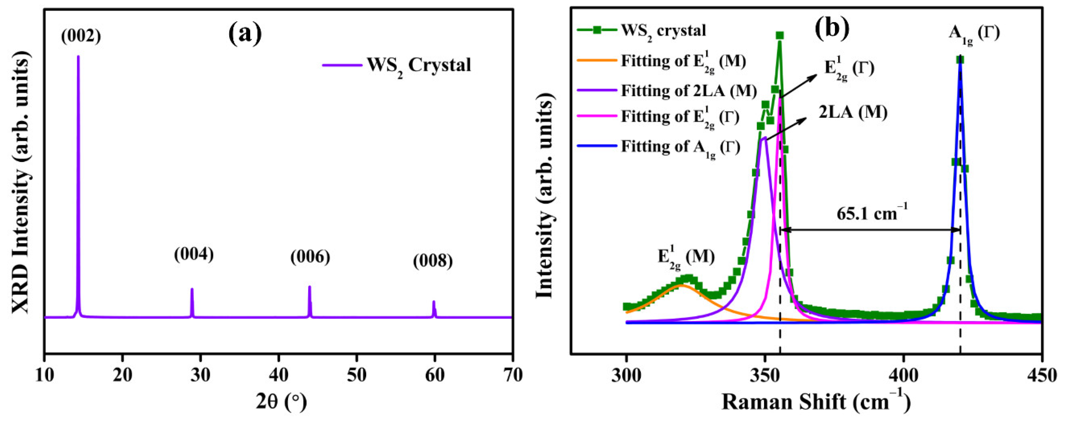
3.1. WS2 Crystal Characterization

The XRD pattern of CVT-grown WS2 crystal is shown in Figure 1a. The observed diffraction peaks at 2θ values of 14.3, 28.9, 43.9, and 59.8° are assigned to the (002), (004), (006), and (008) planes, respectively. The positions of sharp Bragg reflections confirm the 2H phase of WS2 crystals according to JCPDS card no. 08-0237 [42,43]. The 2H WS2 crystal lattice belongs to the P63/mmc ( D 6 h 4 ) hexagonal space group that has space inversion symmetry [44]. The observed sharp and narrow peaks are an indication of the high crystal quality of WS2 crystals grown by the CVT technique. All diffraction peaks along the (00l) direction denote that the crystal growth is along the c-axis and the major preferential orientation is along the (002) plane. The absence of any binary or impurity phases in the XRD pattern demonstrates the exceptional quality of the CVT-grown crystals.
Figure 1b depicts the Raman spectrum of CVT-grown WS2 layered crystal. The multi-peak Lorentzian fitting is used for the individual peaks fitting and also for the deconvolution of a broad peak obtained at around 350 cm−1, which clearly separates the individual peaks from the overlapping. The observed Raman peaks at 319.9, 349.3, 355.1, and 420.2 cm−1 are attributed to E 2 g 1 (M), 2LA (M), E 2 g 1 (Γ), and A 1 g (Γ) modes of WS2 crystal, respectively [45,46,47]. The first-ordered dominant modes E 2 g 1 (Γ) and A 1 g (Γ) are most commonly observed for 2H WS2 crystals [43,44,48]. The E 2 g 1 mode is due to the in-plane vibrations of tungsten and sulfur atoms in the opposite direction, and the A 1 g mode is due to the out-of-plane vibrations in sulfur atoms. The separation between these two modes is 65.1 cm−1, which is consistent with the bulk WS2, and the separation reduces gradually with the decrease of the number of layers [48,49]. The second-order longitudinal acoustic mode 2LA (M) is very close to the E 2 g 1 (Γ) and sometimes it overlaps the E 2 g 1 (Γ) mode [45]. The full-width half maxima of 2LA, E 2 g 1 , and A 1 g modes are 8.3, 3.4, and 3.7 cm−1, respectively, and it denotes the high crystallinity of WS2 crystals grown by the CVT technique.

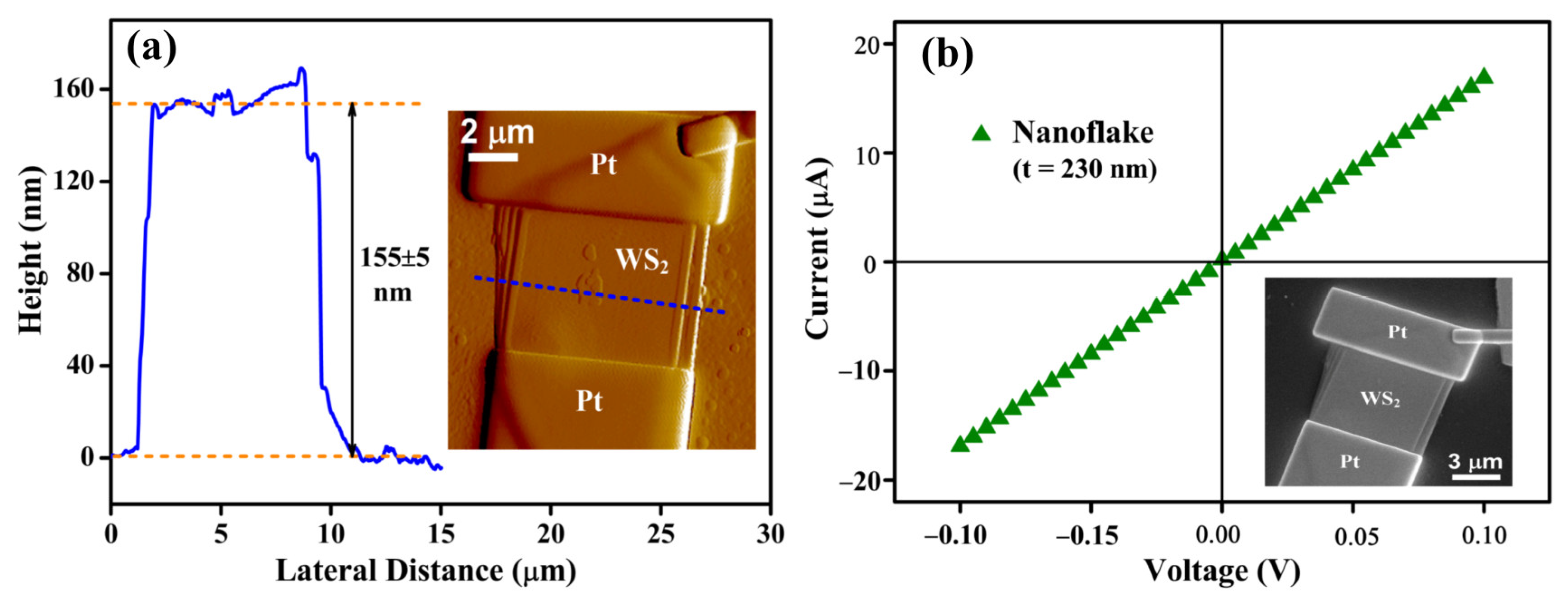
3.2. WS2 Nanoflake Device Characterization

The thickness of the WS2 nanoflakes was calculated using the AFM height profile measurement as shown in Figure 2a. The thickness of a typical nanoflake is 155 ± 5 nm. The inset of Figure 2a shows the AFM picture of the WS2 nanoflake device with Pt contacts. The blue dotted line across the device denotes the position of the height profile measurement. Figure 2b depicts the id-V characteristics of a typical WS2 nanoflake device in the range of −0.1 to +0.1 V. The linear id-V curve confirms the ohmic contact between the WS2 nanoflake and FIB-deposited Pt contacts. The inset of Figure 2b represents the SEM image of the WS2 nanoflake device that is used to calculate the dimensions of the device. The conductivity (σ) of the WS2 nanoflake with a thickness of 230 nm was calculated using the relation [50,51]
σ = G l A = G l w t
where G is the electrical conductance and l, w, and t are the length, width, and thickness of the conduction channel. G is given by I/V, which is obtained from the slope of id-V curve, and the value is 1.69 × 10⁻⁴ Ω−1. The l and w are 4.22 μm and 2.65 μm, respectively, obtained from the SEM image of the nanoflake device with a thickness of 230 nm. The calculated conductivity of a typical nanoflake is 12 Ω−1cm−1.

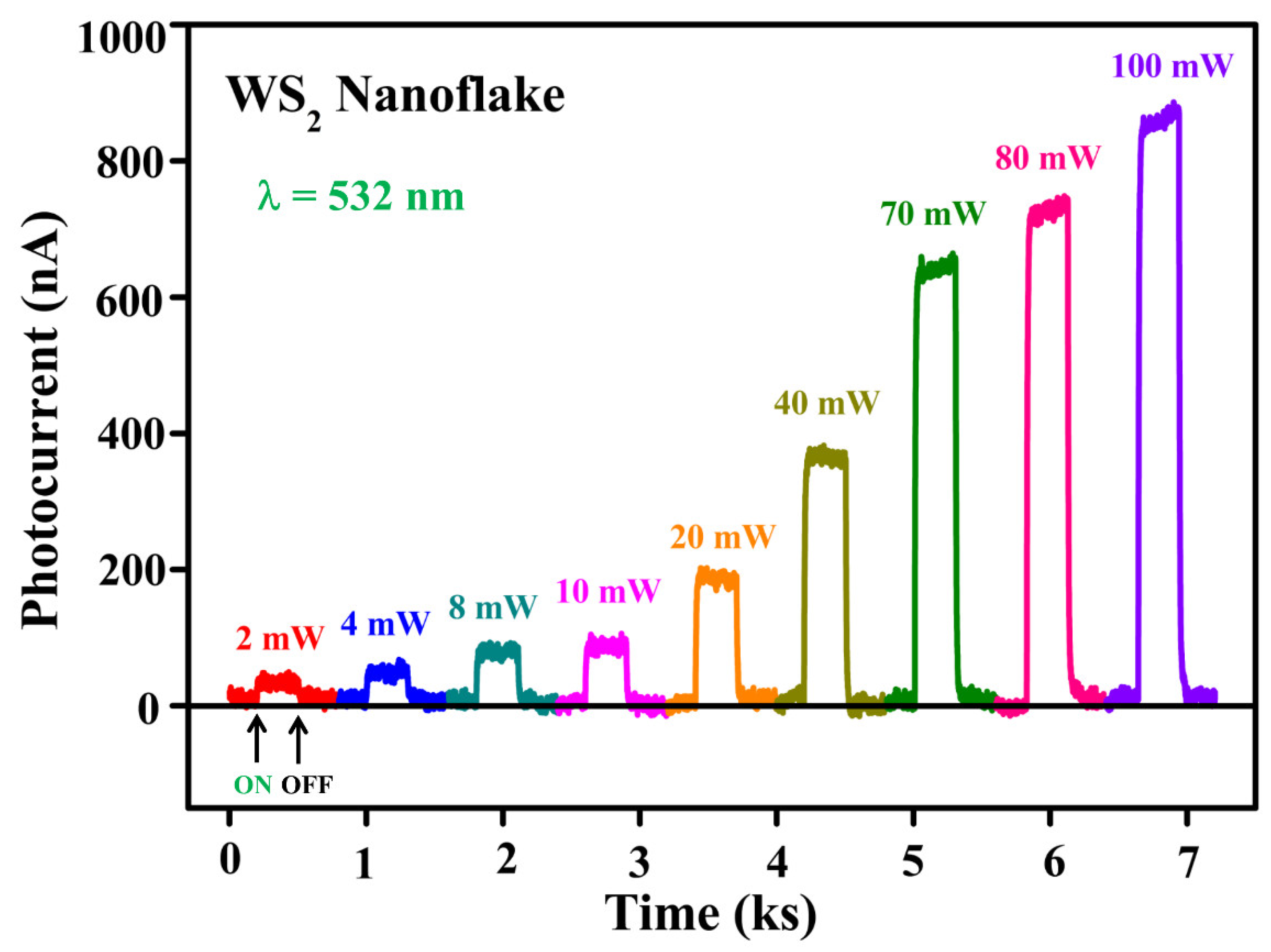
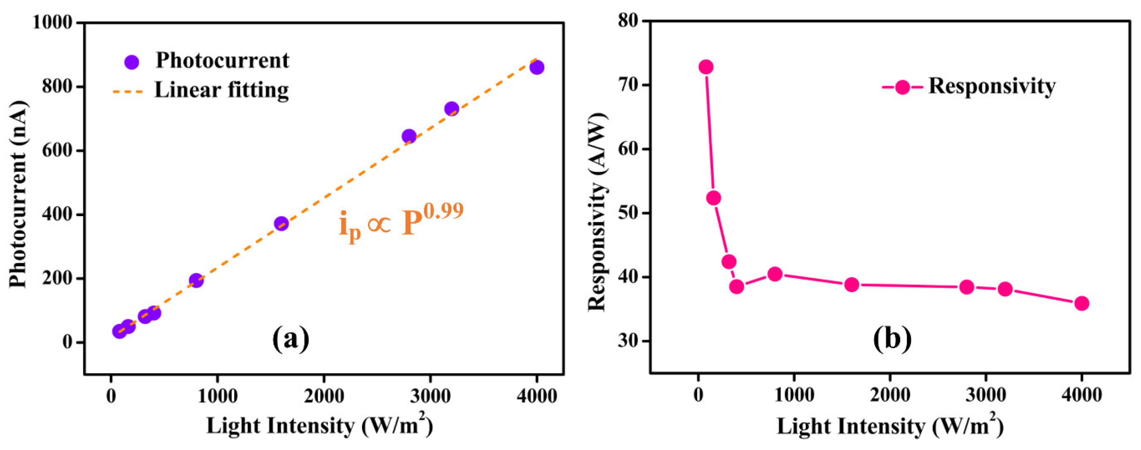
3.3. Photoconduction Properties of WS2 Nanoflake

Figure 3 depicts the photoresponse of a WS2 nanoflake with a thickness of 25 nm modulated by light power at an excitation wavelength of 532 nm. The photocurrent was measured for different light powers varying from 2 to 100 mW. A constant biasing voltage of 1 V was applied for the measurement of photocurrent as a function of time. First, we have recorded one cycle of photocurrent response for each light power separately. Next, the photocurrent measurements of different powers were combined to clearly present the change in photocurrent with respect to different powers. The ON and OFF states denote the laser light conditions for single light power. When the laser was turned on, the photocurrent increased quickly, and we waited until it saturated. Once it reached saturation, the laser was turned off, and the photocurrent was dropped immediately and then reached saturation. The background dark current was subtracted from photoresponse curves to represent the photocurrent curves. It is clear from the photoresponse curves that the photocurrent increases with the increase of light power. Generally, a large number of photons of high light intensity create a higher number of electron-hole pairs, and thus the photocurrent increases. The periodic nature of the photoresponse curve under different light powers is an indication of good stability and reproducibility of fabricated WS2 devices. With the increase of light power up to 100 mW, we did not observe any photocurrent saturation in the WS2 nanoflake, and hence the WS2 photodetectors can be suitable for operation in the linear region.
To interpret the significant dependence of the photocurrent on the illumination intensity, the plot drawn between the photocurrent and light intensity in the range of 80–4000 Wm−2 is shown in Figure 4a. The photocurrent strongly depends on the light intensity, and the experimental data can be fitted using a power law given by i p = a P β , where ip is the photocurrent, a is the scaling constant, P is the light power, and β is an exponent [52]. The power law is well-fitted to the experimental data with β = 0.99. Generally, β values are in the range of 0 to 1. The deviation of the β value from unity is the indication of the presence of complex processes such as generation, trapping, and recombination of electron-hole within the semiconductor [53]. In our case, the β value is near unity, which indicates that the exfoliated WS2 nanoflake was of high quality with very few defects [54].
The photodetectors were characterized by several crucial parameters such as responsivity (R), gain (Γ), and normalized gain ( Γ n ) to evaluate their performance. The R is one of the most important figure-of-merits, which is a measure of the photodetector’s electrical response to the incident light and is obtained from the formula [7]
R = i p P
where, ip is the photocurrent and P is the laser power incident on the projected area (A) of a photodetector, and it is given by P = I A = I w l , where I is the light intensity and w and l are the width and length of the conducting channel, respectively [55]. The R values as a function of light intensity are shown in Figure 4b. We noted that R is sensitive to the lower light intensity (80–320 Wm−2) and insensitive to the higher light intensities (400–4000 Wm−2). R decreases with the increase of light intensity from 80 to 400 Wm−2, and a further increase of light intensity up to 4000 Wm−2 results in an almost constant R value. A similar dependency of R on light intensity was observed in WS2 monolayer [56] and SnS/rGO [57] photodetectors. The calculated R values are in the range of 36–73 AW−1, and this high responsivity may be due to the efficient absorption and optimized WS2 nanoflake device configuration. These values are higher than the other photodetectors based on 2D materials such as NbSe2 nanoflakes (R~2.3–3.8 AW−1) [50], MoS2 nanoflakes (R~20–30 AW−1) [58], and NbS2 nanoflakes (R~0.6 AW−1) [59]. The largest R value (73 AW−1) at lower light intensity (80 Wm−2) is owed to the weak recombination of photo-excited carriers [60].
Gain ( Γ ) is another figure-of-merit of photodetectors that determine the circulating number of photo carriers moving through a photoconductor per unit time before recombination. It is given by the ratio of the carrier lifetime ( τ ) to the transit time ( τ t ) between the electrodes [50,61].
Γ = τ τ t = V l 2 τ μ
where, l is the electrodes inter distance, μ is the mobility, and V is the applied voltage. Γ linearly depends on R and it can be calculated using the formula [62,63]
Γ = R η h ν q
where, η is the external quantum efficiency, q is the charge of an electron, h is Planck’s constant, and ν is the frequency of the photon. The η value was calculated using the formula η = 1 e α t , where α is the absorption coefficient at the wavelength of 532 nm (2.33 eV) and t is the thickness of the nanoflake [50,58]. The reflection loss was eliminated to simply the η calculation. The α value of WS2 bulk is ~2 × 105 cm−1 at a photon energy of 2.33 eV [64,65]. By considering the nanoflake thickness of 25 nm, the calculated η value is 0.39 (39%).
The determined Γ values as a function of light intensity are shown in Figure 5a. The Γ values follow a similar trend to R. The obtained Γ values are in the range of 215–436, with variation of light intensity from 80 to 4000 Wm−2. The Γ decreases with the increase of light intensity up to 400 Wm−2, and a further increase of light intensity up to 4000 Wm−2 leads to saturation in the Γ values. This may be attributed to the continuous filling of trap states upon illumination. Suppose the trap states are filled completely at a certain intensity of light, the excess electrons created by the higher light intensity cannot be trapped and thus decrease the average carrier lifetime. Hence, the photoconductive gain was reduced [4]. The Γ values (215–436) of our photodetector are superior to the reported photodetectors based on the MoS2 nanoflake (Γ~66–103) [58], WS2/Au NPs (Γ~30) [66], and the phototransistors based on MoS2 (Γ~0.2) and MoSe2 (Γ~5 × 10⁻⁴) [67].
Normalized gain ( Γ n ) is independent of device geometry and can be considered a fair figure-of-merit to compare the performance of other devices. The photoconduction process is mainly involving the light absorption and movement of carriers between the electrodes. Numerous factors including carrier mobility, lifetime, applied bias, distance between electrodes, and efficiency of light absorption may affect the performance of photodetectors. Γ n is a measure of the intrinsic photoconductivity of the device and is given by the product of η, τ, and µ [61,68].
Γ n = η τ μ = η Γ V / l 2 = E q l 2 V R
Figure 5b depicts the Γ n values as a function of light intensity. The Γ n values follow the Γ trend and the calculated values are in the range of 3.5–7.3 × 10⁻⁶ cm2V−1. The obtained values are higher than the AuNRs/MoS2/graphene device ( Γ n ~8.63 × 10⁻⁷ cm2V−1) [68] but lower than the MoS2-UCNP nanocomposite ( Γ n ~1.48 × 10⁻⁴ cm2V−1) [61] and InSe ( Γ n ~3.2 cm2V−1) [55] based photodetectors. The moderate Γ n values of our device required further investigation of other parameters such as carrier lifetime and mobility.
The photodetector parameters Γ and Γ n were rarely investigated for the 2D material photodetectors. Hence, the comparison of devices based on Γ and Γ n becomes tough. We have compared our device performance with other reported WS2 photodetectors fabricated by different methods based on their operation region of wavelength, biasing voltage, and responsivity as summarized in Table 1. It is noticed that the WS2 nanoflake device obtained in the present work shows better responsivity at a lower bias voltage of 1 V. The high responsivity of our device also outperformed some CVD-grown WS2 monolayer-based photodetectors, and hence the WS2 nanoflakes can be a potential candidate for fabricating novel optoelectronic devices.

4. Conclusions

We successfully fabricated a visible photodetector using exfoliated WS2 nanoflakes and explored its photoconduction properties. The photocurrent increases with the increase of light intensity from 80 to 4000 Wm−2 and is well-fitted to the power law with an exponent value of 0.99. The photoresponsivity decreases with the increase of light intensity from 80 to 400 Wm−2, and a further increase of light intensity up to 4000 Wm−2 results in an almost constant R value. The fabricated device showed a stable photoresponse with some reproducible characteristics. The device exhibited good responsivity in the range of 36–73 AW−1, and the normalized gain was in the range of 3.5–7.3 × 10⁻⁶ cm2V−1 at a lower biasing voltage of 1 V. The obtained excellent photodetector parameters suggest a promising application of WS2 nanoflakes in future novel optoelectronic devices.

Author Contributions

Conceptualization, R.-S.C.; methodology, H.K.B. and W.-C.S.; validation, R.-S.C. and H.K.B.; formal analysis, H.K.B.; investigation, W.-C.S., Y.-C.L., R.K.U., R.S. and H.-Y.D.; resources, R.-S.C.; writing—original draft preparation, H.K.B.; writing—review and editing, R.-S.C. and H.-Y.D.; supervision, R.-S.C. and H.-Y.D.; project administration, R.-S.C.; funding acquisition, R.-S.C. and H.-Y.D. All authors have read and agreed to the published version of the manuscript.

Funding

This research was funded by Ministry of Science and Technology (MOST) of Taiwan grant number MOST 111-2112-M-011-004-MY3, MOST 108-2628-M-011-001-MY3, MOST 109-2622-E-011-034, MOST 110-2622-E-011-017, MOST 112-2112-M-131-003, and MOST 111-2112-M-131-003. And the APC was funded by Ministry of Science and Technology (MOST) of Taiwan.

Data Availability Statement

The data presented in this study are available on request from the corresponding author.

Acknowledgments

Authors H.-Y.D. and R.-S.C. thanks the support of the Ministry of Science and Technology (MOST) of Taiwan.

Conflicts of Interest

The authors declare no conflict of interest.

References

  1. Yang, W.; Hu, K.; Teng, F.; Weng, J.; Zhang, Y.; Fang, X. High-Performance Silicon-Compatible Large-Area UV-to-Visible Broadband Photodetector Based on Integrated Lattice-Matched Type II Se/n-Si Heterojunctions. Nano Lett. 2018, 18, 4697–4703. [Google Scholar] [CrossRef] [PubMed]
  2. Basyooni, M.A.; Zaki, S.E.; Alfryyan, N.; Tihtih, M.; Eker, Y.R.; Attia, G.F.; Yılmaz, M.; Ateş, Ş.; Shaban, M. Nanostructured MoS2 and WS2 Photoresponses under Gas Stimuli. Nanomaterials 2022, 12, 3585. [Google Scholar] [CrossRef] [PubMed]
  3. Dam, S.; Saha, A.; Hussain, S. Photoresponse Properties of Thin Films of Vertically Grown WS2 Nanoflakes. Mater. Sci. Eng. B Solid-State Mater. Adv. Technol. 2022, 277, 115587. [Google Scholar] [CrossRef]
  4. Fang, H.; Hu, W. Photogating in Low Dimensional Photodetectors. Adv. Sci. 2017, 4, 1700323. [Google Scholar] [CrossRef] [PubMed]
  5. Xie, C.; Mak, C.; Tao, X.; Yan, F. Photodetectors Based on Two-Dimensional Layered Materials Beyond Graphene. Adv. Funct. Mater. 2017, 27, 1603886. [Google Scholar] [CrossRef]
  6. Ghanghass, A.; Sameera, I.; Bhatia, R. Multi-Layer Growth of Tungsten Disulphide Using Thermal Chemical Vapour Deposition. Mater. Today Proc. 2023, 74, 197–201. [Google Scholar] [CrossRef]
  7. Tan, H.; Fan, Y.; Zhou, Y.; Chen, Q.; Xu, W.; Warner, J.H. Ultrathin 2D Photodetectors Utilizing Chemical Vapor Deposition Grown WS2 with Graphene Electrodes. ACS Nano 2016, 10, 7866–7873. [Google Scholar] [CrossRef]
  8. Choi, W.; Choudhary, N.; Han, G.H.; Park, J.; Akinwande, D.; Lee, Y.H. Recent Development of Two-Dimensional Transition Metal Dichalcogenides and Their Applications. Mater. Today 2017, 20, 116–130. [Google Scholar] [CrossRef]
  9. Wang, H.; Yu, L.; Lee, Y.H.; Shi, Y.; Hsu, A.; Chin, M.L.; Li, L.J.; Dubey, M.; Kong, J.; Palacios, T. Integrated Circuits Based on Bilayer MoS2 Transistors. Nano Lett. 2012, 12, 4674–4680. [Google Scholar] [CrossRef] [Green Version]
  10. Jariwala, D.; Sangwan, V.K.; Lauhon, L.J.; Marks, T.J.; Hersam, M.C. Emerging Device Applications for Semiconducting Two-Dimensional Transition Metal Dichalcogenides. ACS Nano 2014, 8, 1102–1120. [Google Scholar] [CrossRef] [Green Version]
  11. Zhu, W.; Low, T.; Wang, H.; Ye, P.; Duan, X. Nanoscale Electronic Devices Based on Transition Metal Dichalcogenides. 2D Mater. 2019, 6, 032004. [Google Scholar] [CrossRef]
  12. Yin, Z.; Li, H.; Li, H.; Jiang, L.; Shi, Y.; Sun, Y.; Lu, G.; Zhang, Q.; Chen, X.; Zhang, H. Single-Layer MoS2 Phototransistors. ACS Nano 2012, 6, 74–80. [Google Scholar] [CrossRef] [PubMed] [Green Version]
  13. Choi, W.; Cho, M.Y.; Konar, A.; Lee, J.H.; Cha, G.B.; Hong, S.C.; Kim, S.; Kim, J.; Jena, D.; Joo, J.; et al. High-Detectivity Multilayer MoS2 Phototransistors with Spectral Response from Ultraviolet to Infrared. Adv. Mater. 2012, 24, 5832–5836. [Google Scholar] [CrossRef] [PubMed]
  14. Tsai, D.S.; Liu, K.K.; Lien, D.H.; Tsai, M.L.; Kang, C.F.; Lin, C.A.; Li, L.J.; He, J.H. Few-Layer MoS2 with High Broadband Photogain and Fast Optical Switching for Use in Harsh Environments. ACS Nano 2013, 7, 3905–3911. [Google Scholar] [CrossRef]
  15. Aji, A.S.; Solís-Fernández, P.; Ji, H.G.; Fukuda, K.; Ago, H. High Mobility WS2 Transistors Realized by Multilayer Graphene Electrodes and Application to High Responsivity Flexible Photodetectors. Adv. Funct. Mater. 2017, 27, 1703448. [Google Scholar] [CrossRef]
  16. Lan, C.; Li, C.; Yin, Y.; Liu, Y. Large-Area Synthesis of Monolayer WS2 and Its Ambient-Sensitive Photo-Detecting Performance. Nanoscale 2015, 7, 5974–5980. [Google Scholar] [CrossRef] [PubMed]
  17. Li, H.J.W.; Huang, K.; Zhang, Y. Enhanced Photoresponsivity of the GOQDs Decorated WS2 Photodetector. Mater. Res. Express 2019, 6, 045902. [Google Scholar] [CrossRef]
  18. Pawbake, A.S.; Waykar, R.G.; Late, D.J.; Jadkar, S.R. Highly Transparent Wafer-Scale Synthesis of Crystalline WS2 Nanoparticle Thin Film for Photodetector and Humidity-Sensing Applications. ACS Appl. Mater. Interfaces 2016, 8, 3359–3365. [Google Scholar] [CrossRef] [PubMed]
  19. Li, J.; Han, J.; Li, H.; Fan, X.; Huang, K. Large-Area, Flexible Broadband Photodetector Based on WS2 Nanosheets Films. Mater. Sci. Semicond. Process. 2020, 107, 104804. [Google Scholar] [CrossRef]
  20. Yang, Y.; Liu, G.; Li, P.; Zhang, M.; Wang, J.; Hu, W.; Xue, Z.; Di, Z. High-Performance Broadband Tungsten Disulfide Photodetector Decorated with Indium Arsenide Nanoislands. Phys. Status Solidi Appl. Mater. Sci. 2020, 217, 2000297. [Google Scholar] [CrossRef]
  21. Ahmad, H.; Thandavan, T.M.K. Ultraviolet Photoconduction in Tungsten Disulphide Based Schottky Heterostructure Photodetector. Opt. Mater. 2019, 92, 255–261. [Google Scholar] [CrossRef]
  22. Yadav, P.V.K.; Ashok Kumar Reddy, Y. Controlled Two-Step Synthesis of Nanostructured WS2 Thin Films for Enhanced UV–Visible Photodetector Applications. Sens. Actuators A Phys. 2022, 345, 113780. [Google Scholar] [CrossRef]
  23. Rivera, A.M.; Gaur, A.P.S.; Sahoo, S.; Katiyar, R.S. Studies on Chemical Charge Doping Related Optical Properties in Monolayer WS2. J. Appl. Phys. 2016, 120, 105102. [Google Scholar] [CrossRef]
  24. Perrozzi, F.; Emamjomeh, S.M.; Paolucci, V.; Taglieri, G.; Ottaviano, L.; Cantalini, C. Thermal Stability of WS2 Flakes and Gas Sensing Properties of WS2/WO3 Composite to H2, NH3 and NO2. Sens. Actuators B Chem. 2017, 243, 812–822. [Google Scholar] [CrossRef]
  25. Liu, L.; Kumar, S.B.; Ouyang, Y.; Guo, J. Performance Limits of Monolayer Transition Metal Dichalcogenide Transistors. IEEE Trans. Electron. Devices 2011, 58, 3042–3047. [Google Scholar] [CrossRef] [Green Version]
  26. Yao, J.D.; Zheng, Z.Q.; Shao, J.M.; Yang, G.W. Stable, Highly-Responsive and Broadband Photodetection Based on Large-Area Multilayered WS2 Films Grown by Pulsed-Laser Deposition. Nanoscale 2015, 7, 14974–14981. [Google Scholar] [CrossRef] [PubMed]
  27. Esfandiari, M.; Mohajerzadeh, S. Formation of Large Area WS2 Nanosheets Using an Oxygen-Plasma Assisted Exfoliation Suitable for Optical Devices. Nanotechnology 2019, 30, 204. [Google Scholar] [CrossRef] [PubMed]
  28. Park, J.; Lee, W.; Choi, T.; Hwang, S.H.; Myoung, J.M.; Jung, J.H.; Kim, S.H.; Kim, H. Layer-Modulated Synthesis of Uniform Tungsten Disulfide Nanosheet Using Gas-Phase Precursors. Nanoscale 2015, 7, 1308–1313. [Google Scholar] [CrossRef]
  29. Georgiou, T.; Jalil, R.; Belle, B.D.; Britnell, L.; Gorbachev, R.V.; Morozov, S.V.; Kim, Y.J.; Gholinia, A.; Haigh, S.J.; Makarovsky, O.; et al. Vertical Field-Effect Transistor Based on Graphene-WS2 Heterostructures for Flexible and Transparent Electronics. Nat. Nanotechnol. 2013, 8, 100–103. [Google Scholar] [CrossRef]
  30. Huo, N.; Yang, S.; Wei, Z.; Li, S.S.; Xia, J.B.; Li, J. Photoresponsive and Gas Sensing Field-Effect Transistors Based on Multilayer WS2 Nanoflakes. Sci. Rep. 2014, 4, 5209. [Google Scholar] [CrossRef] [Green Version]
  31. Mohan, V.V.; Manuraj, M.; Anjana, P.M.; Rakhi, R.B. WS2 Nanoflowers as Efficient Electrode Materials for Supercapacitors. Energy Technol. 2022, 10, 2100976. [Google Scholar] [CrossRef]
  32. Sheng, Y.; Chen, T.; Lu, Y.; Chang, R.J.; Sinha, S.; Warner, J.H. High-Performance WS2 Monolayer Light-Emitting Tunneling Devices Using 2D Materials Grown by Chemical Vapor Deposition. ACS Nano 2019, 13, 4530–4537. [Google Scholar] [CrossRef] [PubMed]
  33. Hasani, A.; Nguyen, T.P.; Tekalgne, M.; VanLe, Q.; Choi, K.S.; Lee, T.H.; Jung Park, T.; Jang, H.W.; Kim, S.Y. The Role of Metal Dopants in WS2 Nanoflowers in Enhancing the Hydrogen Evolution Reaction. Appl. Catal. A Gen. 2018, 567, 73–79. [Google Scholar] [CrossRef]
  34. Li, Y.; Chernikov, A.; Zhang, X.; Rigosi, A.; Hill, H.M.; Van DerZande, A.M.; Chenet, D.A.; Shih, E.M.; Hone, J.; Heinz, T.F. Measurement of the Optical Dielectric Function of Monolayer Transition-Metal Dichalcogenides: MoS2, MoSe2, WS2, and WSe2. Phys. Rev. B—Condens. Matter Mater. Phys. 2014, 90, 205422. [Google Scholar] [CrossRef] [Green Version]
  35. Palik, E.D. Handbook of Optical Constants of Solids III; Academic Press: San Diego, CA, USA, 1998. [Google Scholar]
  36. Yang, R.; Feng, S.; Xiang, J.; Jia, Z.; Mu, C.; Wen, F.; Liu, Z. Ultrahigh-Gain and Fast Photodetectors Built on Atomically Thin Bilayer Tungsten Disulfide Grown by Chemical Vapor Deposition. ACS Appl. Mater. Interfaces 2017, 9, 42001–42010. [Google Scholar] [CrossRef] [PubMed]
  37. Kim, H.C.; Kim, H.; Lee, J.U.; Lee, H.B.; Choi, D.H.; Lee, J.H.; Lee, W.H.; Jhang, S.H.; Park, B.H.; Cheong, H.; et al. Engineering Optical and Electronic Properties of WS2 by Varying the Number of Layers. ACS Nano 2015, 9, 6854–6860. [Google Scholar] [CrossRef]
  38. Zhao, W.; Ghorannevis, Z.; Chu, L.; Toh, M.; Kloc, C.; Tan, P.-H.; Eda, G. Evolution of Electronic Structure in Atomically Thin Sheets of WS2 and WSe2. ACS Nano 2013, 7, 791–797. [Google Scholar] [CrossRef] [Green Version]
  39. Roy, A.; Kalita, P.; Mondal, B. Structural, Spectroscopic and Electrical Properties of Liquid Phase Exfoliated Few Layered Two-Dimensional Tungsten Disulfide (WS2) Using Anionic Surfactant. J. Mater. Sci. Mater. Electron. 2023, 34, 224. [Google Scholar] [CrossRef]
  40. Hwan Lee, S.; Lee, D.; Sik Hwang, W.; Hwang, E.; Jena, D.; Jong Yoo, W. High-Performance Photocurrent Generation from Two-Dimensional WS2 Field-Effect Transistors. Appl. Phys. Lett. 2014, 104, 193113. [Google Scholar] [CrossRef] [Green Version]
  41. Huo, N.; Kang, J.; Wei, Z.; Li, S.S.; Li, J.; Wei, S.H. Novel and Enhanced Optoelectronic Performances of Multilayer MoS2-WS2 Heterostructure Transistors. Adv. Funct. Mater. 2014, 24, 7025–7031. [Google Scholar] [CrossRef]
  42. Habib, M.; Khalil, A.; Muhammad, Z.; Khan, R.; Wang, C.; Rehman, Z.u.; Masood, H.T.; Xu, W.; Liu, H.; Gan, W.; et al. WX2 (X=S, Se) Single Crystals: A Highly Stable Material for Supercapacitor Applications. Electrochim. Acta 2017, 258, 71–79. [Google Scholar] [CrossRef]
  43. Lin, D.Y.; Shih, Y.T.; Lin, P.C.; Tseng, B.C.; Hwang, S.B.; Kao, M.C. Photoelectric Properties of Pristine and Niobium-Doped Tungsten Disulfide Layered Crystals. Opt. Mater. 2023, 135, 113310. [Google Scholar] [CrossRef]
  44. Lan, C.; Li, C.; Ho, J.C.; Liu, Y. 2D WS2: From Vapor Phase Synthesis to Device Applications. Adv. Electron. Mater. 2021, 7, 2000688. [Google Scholar] [CrossRef]
  45. Zobeiri, H.; Xu, S.; Yue, Y.; Zhang, Q.; Xie, Y.; Wang, X. Effect of Temperature on Raman Intensity of nm-thick WS2: Combined Effects of Resonance Raman, Optical Properties, and Interface Optical Interference. Nanoscale 2020, 12, 6064–6078. [Google Scholar] [CrossRef]
  46. Berkdemir, A.; Gutiérrez, H.R.; Botello-Méndez, A.R.; Perea-López, N.; Elías, A.L.; Chia, C.I.; Wang, B.; Crespi, V.H.; López-Urías, F.; Charlier, J.C.; et al. Identification of Individual and Few Layers of WS2 Using Raman Spectroscopy. Sci. Rep. 2013, 3, 1755. [Google Scholar] [CrossRef] [Green Version]
  47. Sourisseau, C.; Cruege, F.; Fouassier, M.; Alba, M. Second-Order Raman Effects, Inelastic Neutron Scattering and Lattice Dynamics in 2H-WS2. Chem. Phys. 1991, 150, 281–293. [Google Scholar] [CrossRef]
  48. Zeng, H.; Liu, G.B.; Dai, J.; Yan, Y.; Zhu, B.; He, R.; Xie, L.; Xu, S.; Chen, X.; Yao, W.; et al. Optical Signature of Symmetry Variations and Spin-Valley Coupling in Atomically Thin Tungsten Dichalcogenides. Sci. Rep. 2013, 3, 2–6. [Google Scholar] [CrossRef] [Green Version]
  49. Mitioglu, A.A.; Plochocka, P.; Deligeorgis, G.; Anghel, S.; Kulyuk, L.; Maude, D.K. Second-Order Resonant Raman Scattering in Single-Layer Tungsten Disulfide WS2. Phys. Rev. B—Condens. Matter Mater. Phys. 2014, 89, 245442. [Google Scholar] [CrossRef] [Green Version]
  50. Huang, Y.H.; Chen, R.S.; Zhang, J.R.; Huang, Y.S. Electronic Transport in NbSe2 Two-Dimensional Nanostructures: Semiconducting Characteristics and Photoconductivity. Nanoscale 2015, 7, 18964–18970. [Google Scholar] [CrossRef]
  51. Bangolla, H.K.; Siao, M.D.; Huang, Y.H.; Chen, R.S.; Žukauskaitė, A.; Palisaitis, J.; Persson, P.O.Å.; Hultman, L.; Birch, J.; Hsiao, C.L. Composition-Dependent Photoconductivities in Indium Aluminium Nitride Nanorods Grown by Magnetron Sputter Epitaxy. Nanoscale Adv. 2022, 4, 4886–4894. [Google Scholar] [CrossRef]
  52. Zeng, L.; Tao, L.; Tang, C.; Zhou, B.; Long, H.; Chai, Y.; Lau, S.P.; Tsang, Y.H. High-Responsivity UV-Vis Photodetector Based on Transferable WS2 Film Deposited by Magnetron Sputtering. Sci. Rep. 2016, 6, 20343. [Google Scholar] [CrossRef] [Green Version]
  53. Kind, H.; Yan, H.; Messer, B.; Law, M.; Yang, P. Nanowire Ultraviolet Photodetectors and Optical Switches. Adv. Mater. 2002, 14, 158–160. [Google Scholar] [CrossRef]
  54. Hafeez, M.; Gan, L.; Li, H.; Ma, Y.; Zhai, T. Large-Area Bilayer ReS2 Film/Multilayer ReS2 Flakes Synthesized by Chemical Vapor Deposition for High Performance Photodetectors. Adv. Funct. Mater. 2016, 26, 4551–4560. [Google Scholar] [CrossRef]
  55. Yang, H.W.; Hsieh, H.F.; Chen, R.S.; Ho, C.H.; Lee, K.Y.; Chao, L.C. Ultraefficient Ultraviolet and Visible Light Sensing and Ohmic Contacts in High-Mobility InSe Nanoflake Photodetectors Fabricated by the Focused Ion Beam Technique. ACS Appl. Mater. Interfaces 2018, 10, 5740–5749. [Google Scholar] [CrossRef]
  56. Lan, C.; Zhou, Z.; Zhou, Z.; Li, C.; Shu, L.; Shen, L.; Li, D.; Dong, R.; Yip, S.P.; Ho, J.C. Wafer-Scale Synthesis of Monolayer WS2 for High-Performance Flexible Photodetectors by Enhanced Chemical Vapor Deposition. Nano Res. 2018, 11, 3371–3384. [Google Scholar] [CrossRef]
  57. Zhuo, R.; Zuo, S.; Quan, W.; Yan, D.; Geng, B.; Wang, J.; Men, X. Large-Size and High Performance Visible-Light Photodetectors Based on Two-Dimensional Hybrid Materials SnS/RGO. RSC Adv. 2018, 8, 761–766. [Google Scholar] [CrossRef]
  58. Shen, W.C.; Chen, R.S.; Huang, Y.S. Photoconductivities in MoS2 Nanoflake Photoconductors. Nanoscale Res. Lett. 2016, 11, 124. [Google Scholar] [CrossRef] [Green Version]
  59. Huang, Y.H.; Peng, C.C.; Chen, R.S.; Huang, Y.S.; Ho, C.H. Transport Properties in Semiconducting NbS2 nanoflakes. Appl. Phys. Lett. 2014, 105, 093106. [Google Scholar] [CrossRef]
  60. Hao, L.; Wang, Z.; Xu, H.; Yan, K.; Dong, S.; Liu, H.; Du, Y.; Wu, Y.; Liu, Y.; Dong, M. 2D SnSe/Si Heterojunction for Self-Driven Broadband Photodetectors. 2D Mater. 2019, 6, 034004. [Google Scholar] [CrossRef]
  61. Ghosh, S.; Chiang, W.C.; Fakhri, M.Y.; Wu, C.T.; Chen, R.S.; Chattopadhyay, S. Ultrasensitive Broadband Photodetector Using Electrostatically Conjugated MoS2-Upconversion Nanoparticle Nanocomposite. Nano Energy 2020, 67, 104258. [Google Scholar] [CrossRef]
  62. Fan, Y.; Zhou, Y.; Wang, X.; Tan, H.; Rong, Y.; Warner, J.H. Photoinduced Schottky Barrier Lowering in 2D Monolayer WS2 Photodetectors. Adv. Opt. Mater. 2016, 4, 1573–1581. [Google Scholar] [CrossRef]
  63. Zhang, W.; Huang, J.K.; Chen, C.H.; Chang, Y.H.; Cheng, Y.J.; Li, L.J. High-Gain Phototransistors Based on a CVD MoS2 Monolayer. Adv. Mater. 2013, 25, 3456–3461. [Google Scholar] [CrossRef]
  64. Ballif, C.; Regula, M.; Lévy, F. Optical and Electrical Properties of Semiconducting WS2 Thin Films: From Macroscopic to Local Probe Measurements. Sol. Energy Mater. Sol. Cells 1999, 57, 189–207. [Google Scholar] [CrossRef]
  65. Roy, S.; Bermel, P. Electronic and Optical Properties of Ultra-Thin 2D Tungsten Disulfide for Photovoltaic Applications. Sol. Energy Mater. Sol. Cells 2018, 174, 370–379. [Google Scholar] [CrossRef]
  66. Liu, Y.; Huang, W.; Chen, W.; Wang, X.; Guo, J.; Tian, H.; Zhang, H.; Wang, Y.; Yu, B.; Ren, T.L.; et al. Plasmon Resonance Enhanced WS2 Photodetector with Ultra-High Sensitivity and Stability. Appl. Surf. Sci. 2019, 481, 1127–1132. [Google Scholar] [CrossRef]
  67. Chang, Y.H.; Zhang, W.; Zhu, Y.; Han, Y.; Pu, J.; Chang, J.K.; Hsu, W.T.; Huang, J.K.; Hsu, C.L.; Chiu, M.H.; et al. Monolayer MoSe2 Grown by Chemical Vapor Deposition for Fast Photodetection. ACS Nano 2014, 8, 8582–8590. [Google Scholar] [CrossRef] [Green Version]
  68. Tomar, D.S.; Ghosh, S.; Jhan, L.C.; Chattopadhyay, S. Gold Nanorod-Activated Graphene/MoS2 Nanosheet-Based Photodetectors for Bidirectional Photoconductance. ACS Appl. Nano Mater. 2023, 6, 1783–1795. [Google Scholar] [CrossRef]
  69. Chen, Y. Growth of a Large, Single-Crystalline WS2 Monolayer for High-Performance Photodetectors by Chemical Vapor Deposition. Micromachines 2021, 12, 137. [Google Scholar] [CrossRef] [PubMed]
  70. Perea-López, N.; Elías, A.L.; Berkdemir, A.; Castro-Beltran, A.; Gutiérrez, A.H.R.; Feng, S.; Lv, R.; Hayashi, T.; López-Urías, F.; Ghosh, S.; et al. Photosensor Device Based on Few-Layered WS2 Films. Adv. Funct. Mater. 2013, 23, 5511–5517. [Google Scholar] [CrossRef]
Figure 1. Structural characterization of CVT-grown WS2 bulk crystal. (a) X-ray diffraction pattern and (b) Raman spectrum.
Nanomaterials 13 02190 g001
Figure 2. (a) AFM height profile of a WS2 nanoflake with a thickness of 155 nm; inset shows the AFM image of the respective device. (b) id−V curve of a typical WS2 nanoflake with a thickness of 230 nm; inset shows SEM image of the WS2 nanoflake device of thickness 155 nm.
Nanomaterials 13 02190 g002
Figure 3. Photocurrent response of a WS2 nanoflake under laser illumination of a wavelength of 532 nm. The photocurrent is measured as a function of time under various powers at a fixed bias voltage of 1 V. The ON/OFF denotes the laser light condition.
Nanomaterials 13 02190 g003
Figure 4. The dependence of (a) photocurrent and (b) responsivity on incident light intensities from 80 to 4000 Wm−2. The photocurrent data points were fitted using linear function.
Nanomaterials 13 02190 g004
Figure 5. Variation of (a) gain and (b) normalized gain of a WS2 nanoflake photodetector with a variation of light intensity from 80 to 4000 Wm−2.
Nanomaterials 13 02190 g005
Table 1. Comparison of WS2 photodetectors based on responsivity, fabrication method, and their operational wavelength with bias voltage.
MaterialFabrication MethodWavelength (nm)Bias Voltage (V)Responsivity (AW−1)Reference
WS2 nanoflakeExfoliation532173Present work
WS2 nanosheetsHydrothermal intercalation53254 × 10−3[19]
WS2 filmsPLD63590.51[26]
WS2 nanofilmSputtering365553.3[52]
WS2 monolayerCVD532100.52 × 10−3[56]
WS2 monolayerCVD50017.3[69]
WS2 multilayerCVD458–647592 × 10−6[70]
Disclaimer/Publisher’s Note: The statements, opinions and data contained in all publications are solely those of the individual author(s) and contributor(s) and not of MDPI and/or the editor(s). MDPI and/or the editor(s) disclaim responsibility for any injury to people or property resulting from any ideas, methods, instructions or products referred to in the content.

