

The Ultra-Large-Bandwidth Cascade Full-Stokes-Imaging Metasurface Based on the Dual-Major-Axis Circular Dichroism Grating
Abstract
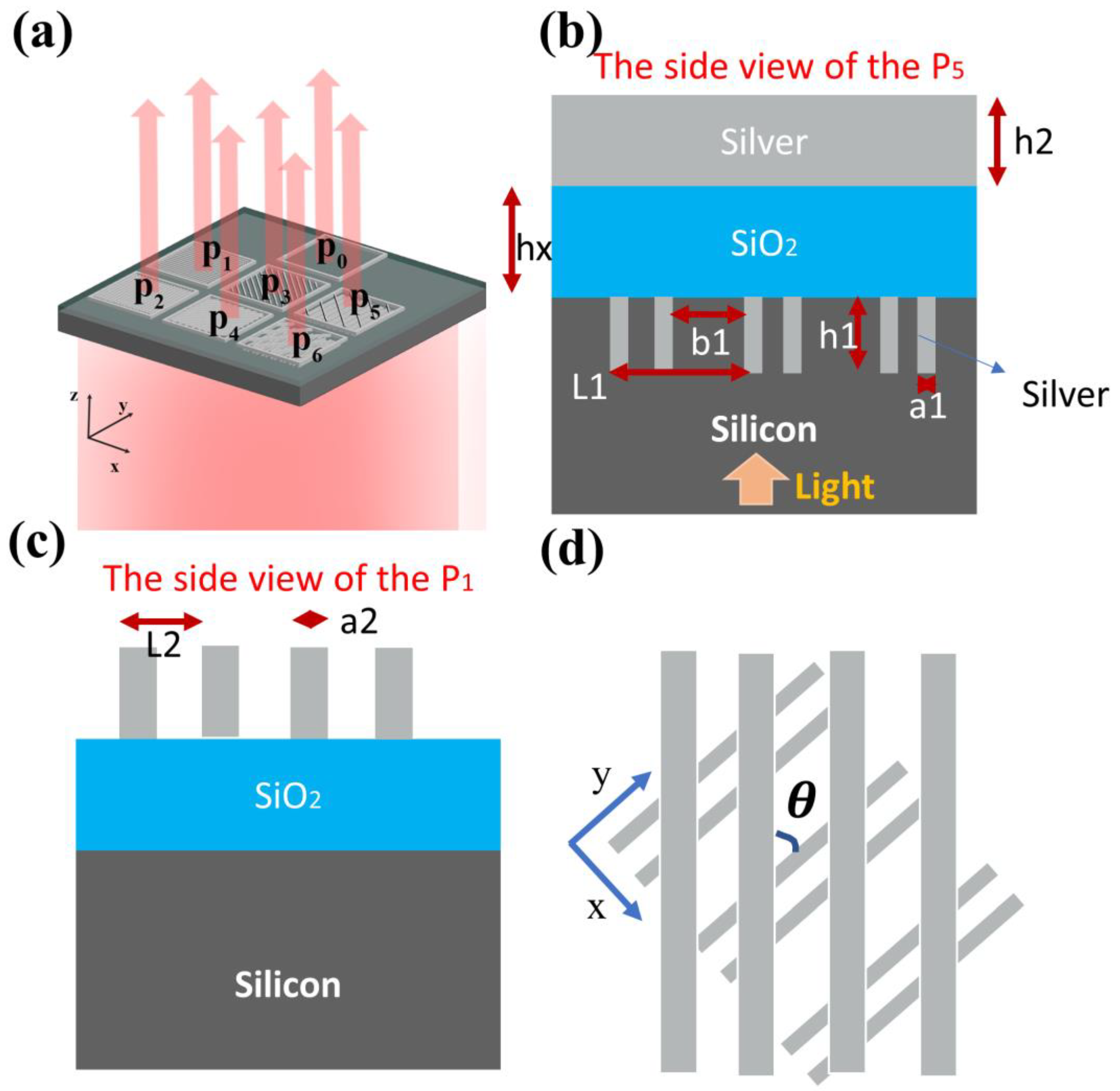
1. Introduction
2. Materials and Methods
3. Results
3.1. The Jones Matrix of the Device
3.2. The Error Analysis of the Full Stokes Pixel
4. Discussion
5. Conclusions
Author Contributions
Funding
Data Availability Statement
Conflicts of Interest
References
- Shao, H.R.; He, Y.H.; Li, W.; Ma, H. Polarization-degree imaging contrast in turbid media: A quantitative study. Appl. Opt. 2006, 45, 4491–4496. [Google Scholar] [CrossRef] [PubMed]
- Loksztejn, A.; Dzwolak, W. Vortex-Induced Formation of Insulin Amyloid Superstructures Probed by Time-Lapse Atomic Force Microscopy and Circular Dichroism Spectroscopy. J. Mol. Biol. 2010, 395, 643–655. [Google Scholar] [CrossRef]
- Li, W.; Coppens, Z.J.; Besteiro, L.V.; Wang, W.Y.; Govorov, A.O.; Valentine, J. Circularly polarized light detection with hot electrons in chiral plasmonic metamaterials. Nat. Commun. 2015, 6, 8379. [Google Scholar] [CrossRef] [PubMed]
- Paniagua-Dominguez, R.; Yu, Y.F.; Khaidarov, E.; Choi, S.M.; Leong, V.; Bakker, R.M.; Liang, X.N.; Fu, Y.H.; Valuckas, V.; Krivitsky, L.A.; et al. A Metalens with a Near-Unity Numerical Aperture. Nano Lett. 2018, 18, 2124–2132. [Google Scholar] [CrossRef]
- Arbabi, A.; Horie, Y.; Bagheri, M.; Faraon, A. Dielectric metasurfaces for complete control of phase and polarization with subwavelength spatial resolution and high transmission. Nat. Nanotechnol. 2015, 10, 937-U190. [Google Scholar] [CrossRef]
- Arbabi, A.; Horie, Y.; Ball, A.J.; Bagheri, M.; Faraon, A. Subwavelength-thick lenses with high numerical apertures and large efficiency based on high-contrast transmitarrays. Nat. Commun. 2015, 6, 7069. [Google Scholar] [CrossRef]
- Farlow, C.A.; Chenault, D.B.; Pezzaniti, J.L.; Spradley, K.D.; Gulley, M.G. Imaging polarimeter developments and applications. In Proceedings of the Conference on Polarization Analysis, Measurement and Remote Sensing IV, San Diego, CA, USA, 29–31 July 2001; pp. 118–125. [Google Scholar]
- Ju, H.J.; Ren, L.Y.; Liang, J.; Qu, E.S.; Bai, Z.F. Method for Mueller matrix acquisition based on a division-of-aperture simultaneous polarimetric imaging technique. J. Quant. Spectrosc. Radiat. Transf. 2019, 225, 39–44. [Google Scholar] [CrossRef]
- Kemme, S.A.; Cruz-Cabrera, A.A.; Nandy, P.; Boye, R.R.; Wendt, J.R.; Carter, T.R.; Samora, S. Micropolarizer alerrays in the MWIR for snapshot polarimetric Imaging. In Proceedings of the Conference on Micro (MEMS) and Nanotechnologies for Defense and Security, Orlando, FL, USA, 10–12 April 2007. [Google Scholar]
- Yu, M.; Cao, L.; Li, L.; Dong, L.T.; Wang, L.; Chen, X.; Song, Z.X.; Weng, Z.K.; Wang, Z.B. Fabrication of Division-of-focal-plane Polarizer Arrays by Electron Beam Lithography. In Proceedings of the 2017 7th International Conference on Manipulation, Manufacturing and Measurement on the Nanoscale (3M-NANO), Shanghai, China, 7–11 August 2017; pp. 79–82. [Google Scholar]
- Yan, C.; Li, X.; Pu, M.B.; Ma, X.L.; Zhang, F.; Gao, P.; Liu, K.P.; Luo, X.G. Midinfrared real-time polarization imaging with all-dielectric metasurfaces. Appl. Phys. Lett. 2019, 114, 161904. [Google Scholar] [CrossRef]
- Mueller, J.P.B.; Rubin, N.A.; Devlin, R.C.; Groever, B.; Capasso, F. Metasurface Polarization Optics: Independent Phase Control of Arbitrary Orthogonal States of Polarization. Phys. Rev. Lett. 2017, 118, 113901. [Google Scholar] [CrossRef] [PubMed]
- Rubin, N.A.; D’Aversa, G.; Chevalier, P.; Shi, Z.J.; Chen, W.T.; Capasso, F. Matrix Fourier optics enables a compact full-Stokes polarization camera. Science 2019, 365, eaax1839. [Google Scholar] [CrossRef] [PubMed]
- Zhu, A.Y.; Chen, W.T.; Zaidi, A.; Huang, Y.W.; Khorasaninejad, M.; Sanjeev, V.; Qiu, C.W.; Capasso, F. Giant intrinsic chiro-optical activity in planar nanostructures. In Proceedings of the Conference on Lasers and Electro-Optics (CLEO), San Jose, CA, USA, 13–18 May 2018. [Google Scholar]
- Benedetti, A.; Alam, B.; Esposito, M.; Tasco, V.; Leahu, G.; Belardin, A.; Voti, R.L.; Passaseo, A.; Sibilia, C. Precise detection of circular dichroism in a cluster of nano-helices by photoacoustic measurements. Sci. Rep. 2017, 7, 5257. [Google Scholar] [CrossRef]
- Esposito, M.; Tasco, V.; Todisco, F.; Cuscuna, M.; Benedetti, A.; Sanvitto, D.; Passaseo, A. Triple-helical nanowires by tomographic rotatory growth for chiral photonics. Nat. Commun. 2015, 6, 6484. [Google Scholar] [CrossRef]
- Esposito, M.; Manoccio, M.; Leo, A.; Cuscuna, M.; Sun, Y.L.; Ageev, E.; Zuev, D.; Benedetti, A.; Tarantini, I.; Passaseo, A.; et al. 3D Chiral MetaCrystals. Adv. Funct. Mater. 2022, 32, 2109258. [Google Scholar] [CrossRef]
- Chen, W.B.; Rui, G.H.; Abeysinghe, D.C.; Nelson, R.L.; Zhan, Q.W. Hybrid spiral plasmonic lens: Towards an efficient miniature circular polarization analyzer. Opt. Express 2012, 20, 26299–26307. [Google Scholar] [CrossRef]
- Bachman, K.A.; Peltzer, J.J.; Flammer, P.D.; Furtak, T.E.; Collins, R.T.; Hollingsworth, R.E. Spiral plasmonic nanoantennas as circular polarization transmission filters. Opt. Express 2012, 20, 1308–1319. [Google Scholar] [CrossRef]
- Schwanecke, A.S.; Fedotov, V.A.; Khardikov, V.V.; Prosvirnin, S.L.; Chen, Y.; Zheludev, N.I. Nanostructured metal film with asymmetric optical transmission. Nano Lett. 2008, 8, 2940–2943. [Google Scholar] [CrossRef] [PubMed]
- Fedotov, V.A.; Schwanecke, A.S.; Zheludev, N.I.; Khardikov, V.V.; Prosvirnin, S.L. Asymmetric transmission of light and enantiomerically sensitive plasmon resonance in planar chiral nanostructures. Nano Lett. 2007, 7, 1996–1999. [Google Scholar] [CrossRef]
- Hu, J.P.; Zhao, X.N.; Lin, Y.; Zhu, A.J.; Zhu, X.J.; Guo, P.J.; Cao, B.; Wang, C.H. All-dielectric metasurface circular dichroism waveplate. Sci. Rep. 2017, 7, 41893. [Google Scholar] [CrossRef]
- Basiri, A.; Chen, X.H.; Bai, J.; Amrollahi, P.; Carpenter, J.; Holman, Z.; Wang, C.; Yao, Y. Nature-inspired chiral metasurfaces for circular polarization detection and full-Stokes polarimetric measurements. Light-Sci. Appl. 2019, 8, 78. [Google Scholar] [CrossRef]
- Bai, J.; Wang, C.; Chen, X.H.; Basiri, A.; Wang, C.; Yao, Y. Chip-Integrated Plasmonic Flat Optics for Mid-infrared Polarization Detection. In Proceedings of the Conference on Lasers and Electro-Optics (CLEO), San Jose, CA, USA, 13–18 May 2018. [Google Scholar]
- Cheng, B.; Zou, Y.X.; Shao, H.X.; Li, T.; Song, G.F. Full-Stokes imaging polarimetry based on a metallic metasurface. Opt. Express 2020, 28, 27324–27336. [Google Scholar] [CrossRef]
- Pors, A.; Nielsen, M.G.; Bozhevolnyi, S.I. Plasmonic metagratings for simultaneous determination of Stokes parameters. Optica 2015, 2, 716–723. [Google Scholar] [CrossRef]
- Chen, W.T.; Torok, P.; Foreman, M.R.; Liao, C.Y.; Tsai, W.Y.; Wu, P.R.; Tsai, D.P. Integrated plasmonic metasurfaces for spectropolarimetry. Nanotechnology 2016, 27, 224002. [Google Scholar] [CrossRef]
- Jung, M.; Dutta-Gupta, S.; Dabidian, N.; Brener, I.; Shcherbakov, M.; Shvets, G. Polarimetry Using Graphene-Integrated Anisotropic Metasurfaces. ACS Photonics 2018, 5, 4283–4288. [Google Scholar] [CrossRef]
- Lee, K.; Yun, H.; Mun, S.E.; Lee, G.Y.; Sung, J.; Lee, B. Ultracompact Broadband Plasmonic Polarimeter. Laser Photonics Rev. 2018, 12, 1700297. [Google Scholar] [CrossRef]
- Afshinmanesh, F.; White, J.S.; Cai, W.S.; Brongersma, M.L. Measurement of the polarization state of light using an integrated plasmonic polarimeter. Nanophotonics 2012, 1, 125–129. [Google Scholar] [CrossRef]
- Espinosa-Soria, A.; Rodriguez-Fortuno, F.J.; Griol, A.; Martinez, A. On-Chip Optimal Stokes Nanopolarimetry Based on Spin-Orbit Interaction of Light. Nano Lett. 2017, 17, 3139–3144. [Google Scholar] [CrossRef] [PubMed]
- Bai, J.; Wang, C.; Chen, X.H.; Basiri, A.; Wang, C.; Yao, Y. Chip-integrated plasmonic flat optics for mid-infrared full-Stokes polarization detection. Photonics Res. 2019, 7, 1051–1060. [Google Scholar] [CrossRef]
- Arbabi, A.; Faraon, A. Fundamental limits of ultrathin metasurfaces. Sci. Rep. 2017, 7, srep43722. [Google Scholar] [CrossRef]
- Overvig, A.; Yu, N.F.; Alu, A. Chiral Quasi-Bound States in the Continuum. Phys. Rev. Lett. 2021, 126, 073001. [Google Scholar] [CrossRef]
- Kim, K.H.; Kim, J.R. High-Q Chiroptical Resonances by Quasi-Bound States in the Continuum in Dielectric Metasurfaces with Simultaneously Broken In-Plane Inversion and Mirror Symmetries. Adv. Opt. Mater. 2021, 9, 2101162. [Google Scholar] [CrossRef]
- Gandolfi, M.; Tognazzi, A.; Rocco, D.; De Angelis, C.; Carletti, L. Near-unity third-harmonic circular dichroism driven by a quasibound state in the continuum in asymmetric silicon metasurfaces. Phys. Rev. A 2021, 104, 023524. [Google Scholar] [CrossRef]
- Shi, T.; Deng, Z.L.; Geng, G.Z.; Zeng, X.Z.; Zeng, Y.X.; Hu, G.W.; Overvig, A.; Li, J.J.; Qiu, C.W.; Alu, A.; et al. Planar chiral metasurfaces with maximal and tunable chiroptical response driven by bound states in the continuum. Nat. Commun. 2022, 13, 4111. [Google Scholar] [CrossRef] [PubMed]
- Babar, S.; Weaver, J.H. Optical constants of Cu, Ag, and Au revisited. Appl. Opt. 2015, 54, 477–481. [Google Scholar] [CrossRef]
- Cheng, B.; Wang, L.; Zou, Y.X.; Lv, L.F.; Li, C.C.; Xu, Y.; Song, G.F. Large bandwidth and high-efficiency plasmonic quarter-wave plate. Opt. Express 2021, 29, 16939–16949. [Google Scholar] [CrossRef] [PubMed]
- Dionne, J.A.; Sweatlock, L.A.; Atwater, H.A.; Polman, A. Plasmon slot waveguides: Towards chip-scale propagation with subwavelength-scale localization. Phys. Rev. B 2006, 73, 035407. [Google Scholar] [CrossRef]
- Dionne, J.A.; Lezec, H.J.; Atwater, H.A. Highly confined photon transport in subwavelength metallic slot waveguides. Nano Lett. 2006, 6, 1928–1932. [Google Scholar] [CrossRef]
- Yang, B.A.; Ye, W.M.; Yuan, X.D.; Zhu, Z.H.; Zeng, C. Design of ultrathin plasmonic quarter-wave plate based on period coupling. Opt. Lett. 2013, 38, 679–681. [Google Scholar] [CrossRef]
- Hu, X.B.; Li, J.; Wei, X. Resonant cavity enhanced waveguide transmission for broadband and high efficiency quarter-wave plate. Opt. Express 2017, 25, 29617–29626. [Google Scholar] [CrossRef]
- Wang, Y.; Liu, Y.M.; Li, J.; Liu, C.; Yu, Z.Y.; Ye, H.; Yu, L. Broadband Ultrathin Transmission Quarter Waveplate with Rectangular Hole Array Based on Plasmonic Resonances. Nanoscale Res. Lett. 2019, 14, 384–388. [Google Scholar] [CrossRef]
- Zhu, A.J.; Qian, Q.Y.; Yan, Y.; Hu, J.P.; Zhao, X.N.; Wang, C.H. Ultrathin plasmonic quarter waveplate using broken rectangular annular metasurface. Opt. Laser Technol. 2017, 92, 120–125. [Google Scholar] [CrossRef]
- Li, T.; Hu, X.B.; Chen, H.M.; Zhao, C.; Xu, Y.; Wei, X.; Song, G.F. Metallic metasurfaces for high efficient polarization conversion control in transmission mode. Opt. Express 2017, 25, 23597–23604. [Google Scholar] [CrossRef] [PubMed]
- Decker, M.; Klein, M.W.; Wegener, M.; Linden, S. Circular dichroism of planar chiral magnetic metamaterials. Opt. Lett. 2007, 32, 856–858. [Google Scholar] [CrossRef] [PubMed]


| Structure Design | Wavelength | Efficiency (Average) | Bandwidth |
|---|---|---|---|
| L-shaped [42] | 1550 nm | ~0.4 | 80 nm |
| Metal grating [43] | 1450 nm | ~0.4 | 300 nm |
| Rectangular hole [44] | 1500 nm | ~0.4 | ~520 nm |
| Metal [45] | 1550 nm | ~0.4 | 120 nm |
| Metal cross [46] | 1250 nm | 0.85 | ~140 nm |
| Ag grating [39] | 1250 nm | ~0.7 | 600 nm |
| This proposal | 1600 nm | ~0.55 | 1200 nm |
| Structure Design | Operation Mode | Bandwidth | Extinction Ratio (Maximum) | Circular Polarization Dichroism (Average) |
|---|---|---|---|---|
| Plasmonic metasurface [3] | Absorption | m (70 nm) | ~9:1 | |
| Dielectric metasurface [22] | Transmission | 1.48–1.52 μm (40 nm) | 345:1 | 80% |
| Bilayer metasurface [47] | Transmission | (100 nm) | NA | 8% |
| Metal–dielectric hybrid [23] | Transmission | (180 nm) | ~400:1 | ~80% |
| Bilayer metasurface [24] | Transmission | (200 nm) | ~300:1 | 9% |
| U-shaped metasurface [25] | Transmission | (200 nm) | ~1900:1 | ~80% |
| This proposal: | Transmission | 1.20–2.80 μm (1600 nm) | ~100:1 | ~60% |
Disclaimer/Publisher’s Note: The statements, opinions and data contained in all publications are solely those of the individual author(s) and contributor(s) and not of MDPI and/or the editor(s). MDPI and/or the editor(s) disclaim responsibility for any injury to people or property resulting from any ideas, methods, instructions or products referred to in the content. |
© 2023 by the authors. Licensee MDPI, Basel, Switzerland. This article is an open access article distributed under the terms and conditions of the Creative Commons Attribution (CC BY) license (https://creativecommons.org/licenses/by/4.0/).
Share and Cite
Cheng, B.; Song, G. The Ultra-Large-Bandwidth Cascade Full-Stokes-Imaging Metasurface Based on the Dual-Major-Axis Circular Dichroism Grating. Nanomaterials 2023, 13, 2211. https://doi.org/10.3390/nano13152211
Cheng B, Song G. The Ultra-Large-Bandwidth Cascade Full-Stokes-Imaging Metasurface Based on the Dual-Major-Axis Circular Dichroism Grating. Nanomaterials. 2023; 13(15):2211. https://doi.org/10.3390/nano13152211
Chicago/Turabian StyleCheng, Bo, and Guofeng Song. 2023. "The Ultra-Large-Bandwidth Cascade Full-Stokes-Imaging Metasurface Based on the Dual-Major-Axis Circular Dichroism Grating" Nanomaterials 13, no. 15: 2211. https://doi.org/10.3390/nano13152211
APA StyleCheng, B., & Song, G. (2023). The Ultra-Large-Bandwidth Cascade Full-Stokes-Imaging Metasurface Based on the Dual-Major-Axis Circular Dichroism Grating. Nanomaterials, 13(15), 2211. https://doi.org/10.3390/nano13152211