Article

Atomically Thin Amorphous Indium–Oxide Semiconductor Film Developed Using a Solution Process for High-Performance Oxide Transistors

School of Electronic and Electrical Engineering, Kyungpook National University, Daegu 41566, Republic of Korea
*
Authors to whom correspondence should be addressed.
Present address: LG Display, Paju 10845, Republic of Korea.
Nanomaterials 2023, 13(18), 2568; https://doi.org/10.3390/nano13182568
Submission received: 19 August 2023 / Revised: 9 September 2023 / Accepted: 11 September 2023 / Published: 16 September 2023

Abstract

:
High-performance oxide transistors have recently attracted significant attention for use in various electronic applications, such as displays, sensors, and back-end-of-line transistors. In this study, we demonstrate atomically thin indium–oxide (InOx) semiconductors using a solution process for high-performance thin-film transistors (TFTs). To achieve superior field-effect mobility and switching characteristics in TFTs, the bandgap and thickness of the InOx were tuned by controlling the InOx solution molarity. As a result, a high field-effect mobility and on/off-current ratio of 13.95 cm2 V−1 s−1 and 1.42 × 10¹⁰, respectively, were achieved using 3.12-nanometer-thick InOx. Our results showed that the charge transport of optimized InOx with a thickness of 3.12 nm is dominated by percolation conduction due to its low surface roughness and appropriate carrier concentration. Furthermore, the atomically thin InOx TFTs showed superior positive and negative gate bias stress stabilities, which are important in electronic applications. The proposed oxide TFTs could provide an effective means of the fabrication of scalable, high-throughput, and high-performance transistors for next-generation electronic applications.

1. Introduction

Metal–oxide thin-film transistors (TFTs) were introduced for use in displays, sensors, and back-end-of-line (BEOL) transistors due to their various advantages, such as low processing temperature, high mobility, low subthreshold swing (SS), optical transparency, and high mechanical flexibility [1,2,3]. Oxide semiconductors in the solution process have attracted a lot of attention because they enable low-cost and high-throughput manufacturing, although sputtered amorphous indium–gallium–zinc–oxide semiconductors are more widely used in industry due to their high uniformity, good electrical performance, and bias stability [4,5,6]. Unfortunately, it is difficult to fabricate high-performance amorphous oxide TFTs using the solution process. Although multicomponent metal oxides are usable to form the amorphous phase, which leads to high uniformity and yield in mass production, a high annealing temperature of over 300 °C is generally required to promote metal–oxygen–metal condensation and densification in solution-processed multicomponent oxide TFTs [7,8]. In addition, semiconductors with relatively low electron mobility are produced via this process due to the poor quality of the solution-processed films compared to vacuum-processed films.
To overcome these issues, various attractive methods have been proposed in terms of the fabrication process, synthesis, and device configuration. For example, combustion synthesis and photochemical activation were introduced for low-temperature fabrications [5,9,10]. Heterostructure semiconductors and various metal doping strategies were proposed to create high-performance transistors [11,12]. With similar goals in mind, various oxide materials have been suggested. Indium oxide (InOx) is one of the most desirable semiconducting materials due to its high intrinsic electron mobility and relatively low activation temperature (200–300 °C) [13,14]. Despite these advantages, its poor switching characteristics with high off-current and the polycrystalline structure are critical obstacles to the practical use of InOx TFTs. Controlling the semiconductor thickness at the atomic scale allows the effective tuning of the bandgap and carrier concentration of the semiconductor, thereby enabling the achievements in terms of reasonable switching characteristics, mobility, and bias stability in transistors [15]. Atomic-layer-deposited high-quality InOx of several nanometers in thickness have been reported for BEOL-compatible transistors [3,16]. However, the formation of atomically thin amorphous InOx semiconductors through a low-temperature solution process and the high-performance amorphous oxide transistor based on it have not yet been thoroughly studied.
In this study, we address these challenges by developing a solution-deposited ultrathin amorphous InOx semiconductor. By controlling the molarity of the solution, InOx semiconductors were deposited at various thicknesses in the range 1.95–5.51 nm. Their crystallinities, bandgaps, atomic bonding states, and electrical characteristics are also presented. Despite being fabricated in a solution processed at a low temperature of 300 °C, InOx TFTs with optimal thicknesses of about 3 nm exhibited high field-effect mobility (μFE) and an on/off-current ratio (Ion/off) of 13.95 cm2 V−1 s−1 and 1.42 × 10¹⁰, respectively. We show that the charge transport of the roughly 3-nanometer-thick low-dimensional InOx is dominated by percolation conduction due to low surface roughness and appropriate carrier concentration. The bias stability values of atomically thin InOx-based TFTs are also investigated. This achievement shows the possibility of overcoming the limitations of high-mobility semiconductor materials and solution processes.

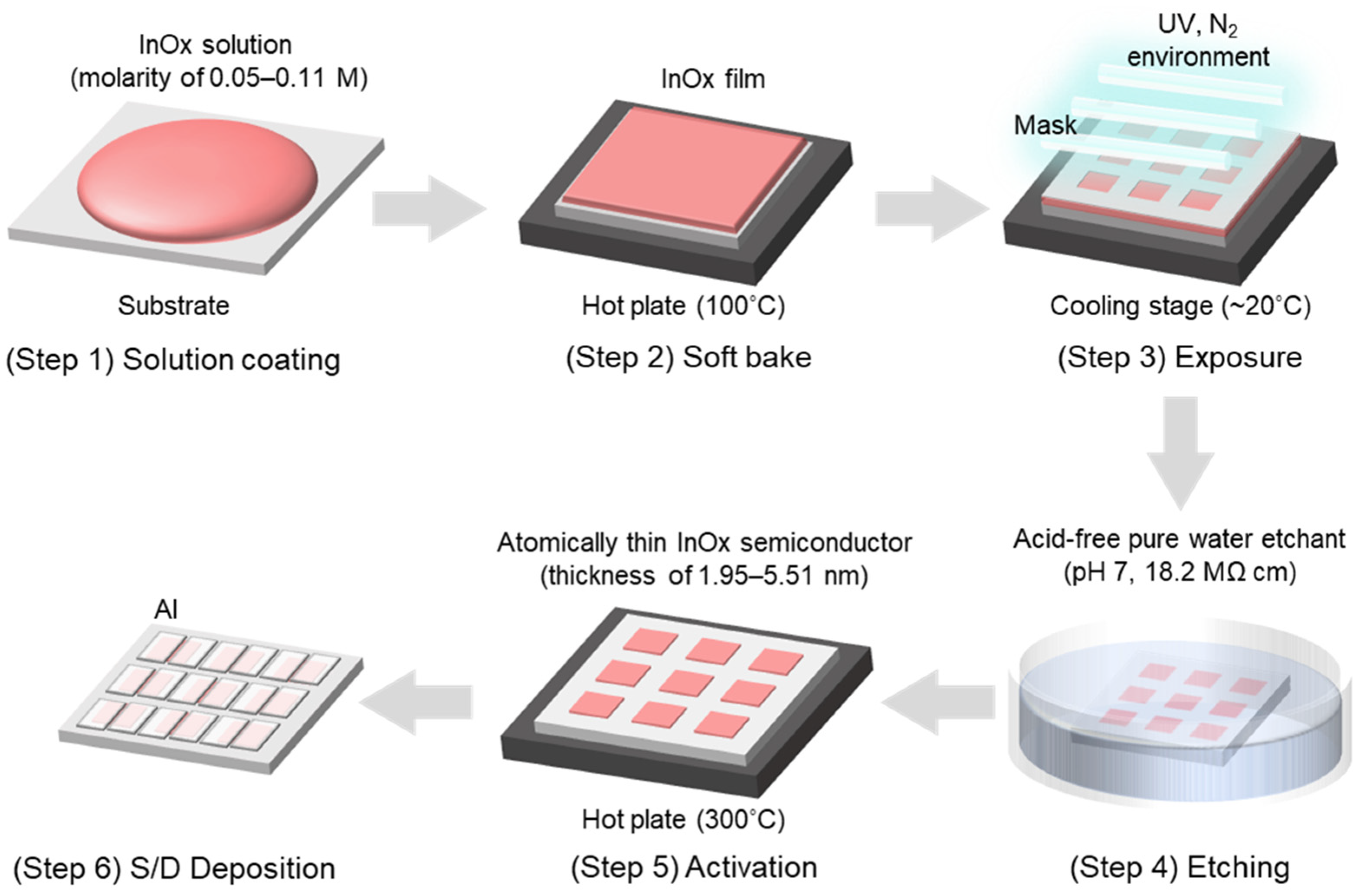
2. Materials and Methods

2.1. Preparation of Oxide Precursor Solutions

InOx precursor solutions were prepared for the fabrication of oxide semiconductors. InOx solutions were prepared by dissolving In(NO3)3·xH2O (Sigma-Aldrich, St. Louis, MO, USA) 2-methoxyethanol at various molarities of 0.05, 0.07, 0.09, and 0.11. All solutions were stirred at a room temperature of 25 °C for 30 min to obtain clear and homogeneous solutions.

2.2. Fabrication of TFTs

Si/SiO2 wafers were cleaned using sonication for 10 min each in acetone, isopropyl alcohol, and deionized (DI) water. The residual moisture on the cleaned substrates was removed via drying with N2 and annealing at 300 °C for 30 min. We previously reported the use of a water etchant-based photopatterning method to deposit the patterned low-defect oxide thin films, which is compatible with the solution process [17]. In this study, water etchant-based photopatterning was used to deposit the high-quality InOx semiconductors. Figure 1 displays a schematic of the process of the fabrication of oxide TFTs. InOx solution was spin coated at 3000 rpm for 20 s on a cleaned wafer (Step 1). The InOx-deposited wafer was then soft baked at 100 °C for 30 s (Step 2). Afterward, a fine metal mask was covered for selective exposure to ultraviolet (UV) light for 60–120 s in an N2 environment (Step 3). UV irradiation (25 mW cm−2) was conducted via a low-pressure mercury lamp with two main wavelengths, namely 253.7 (90%) and 184.9 nm (10%). Consecutively, the wafer was developed in a DI water etchant for 1 min (Step 4). Finally, clearly patterned InOx was subsequentially annealed at 100 °C for 10 min and 300 °C for 2 h on a hot plate in air (Step 5). In this series of processes, UV photons induced the photochemical cleavage of alkoxy groups and decomposition nitrate ligands; therefore, the UV-irradiated parts remained in the etching process. Also, water molecules were sufficiently supplied to the InOx semiconductor during the etching process, thereby enabling effective hydrolysis and condensation reactions at the annealing stage, as shown in Figure S1. As a result, the reactions promote the densification and defect reduction in InOx, which are advantageous for high-performance oxide transistors [17]. The final InOx thicknesses obtained were in the range 1.95–5.51 nm depending on the solution molarity. The 50-nanometer-thick Al was deposited using thermal evaporation for source and drain electrodes. The channel length (L) and width (W) were 100 and 1000 μm, respectively. Here, the molarities of InOx were 0.05, 0.07, 0.09, and 0.11, and the corresponding InOx thin films and TFTs were named InOx-5, InOx-7, InOx-9, and InOx-11, respectively.

2.3. Analysis of Thin Films and Devices

Transmission electron microscopy (TEM; FEI Company, Hillsboro, OR, USA, Titan G2 ChemiSTEM Cs Probe) was used to observe the film’s thickness, crystallinity, and elemental mapping. The surface morphologies of the atomically thin InOx were observed using non-contact-mode atomic force microscopy (AFM; Park Systems, NX20, Suwon, Republic of Korea). The chemical compositions of the InOx were analyzed using X-ray photoelectron spectroscopy (XPS; ThermoFisher Scientific, NEXSA, Waltham, MA, USA) with an Al Kα (1486.6 eV) X-ray source. UV–Visible (UV–Vis) spectrophotometry (Perkin Elmer, LAMBDA 265, Waltham, MA, USA) was measured to understand the effects of thickness at the atomic scale on the optical bandgap of InOx. Grazing incidence X-ray diffraction (GIXRD) (Bruker, D8 Discover, Billerica, MA, USA) tests were carried out using Cu Kα radiation and a small incident angle of 0.5° to investigate the crystalline phase characteristics of InOx. The electrical characteristics and bias stabilities of the InOx TFTs were measured using a probe station (MS Tech, model 4000, Seoul, Republic of Korea) with a precision LCR meter (Agilent E4980A, Santa Clara, CA, USA) and a semiconductor parameter analyzer (Keithley 2636B, Cleveland, OH, USA). All devices were measured at room temperature in a dark environment.

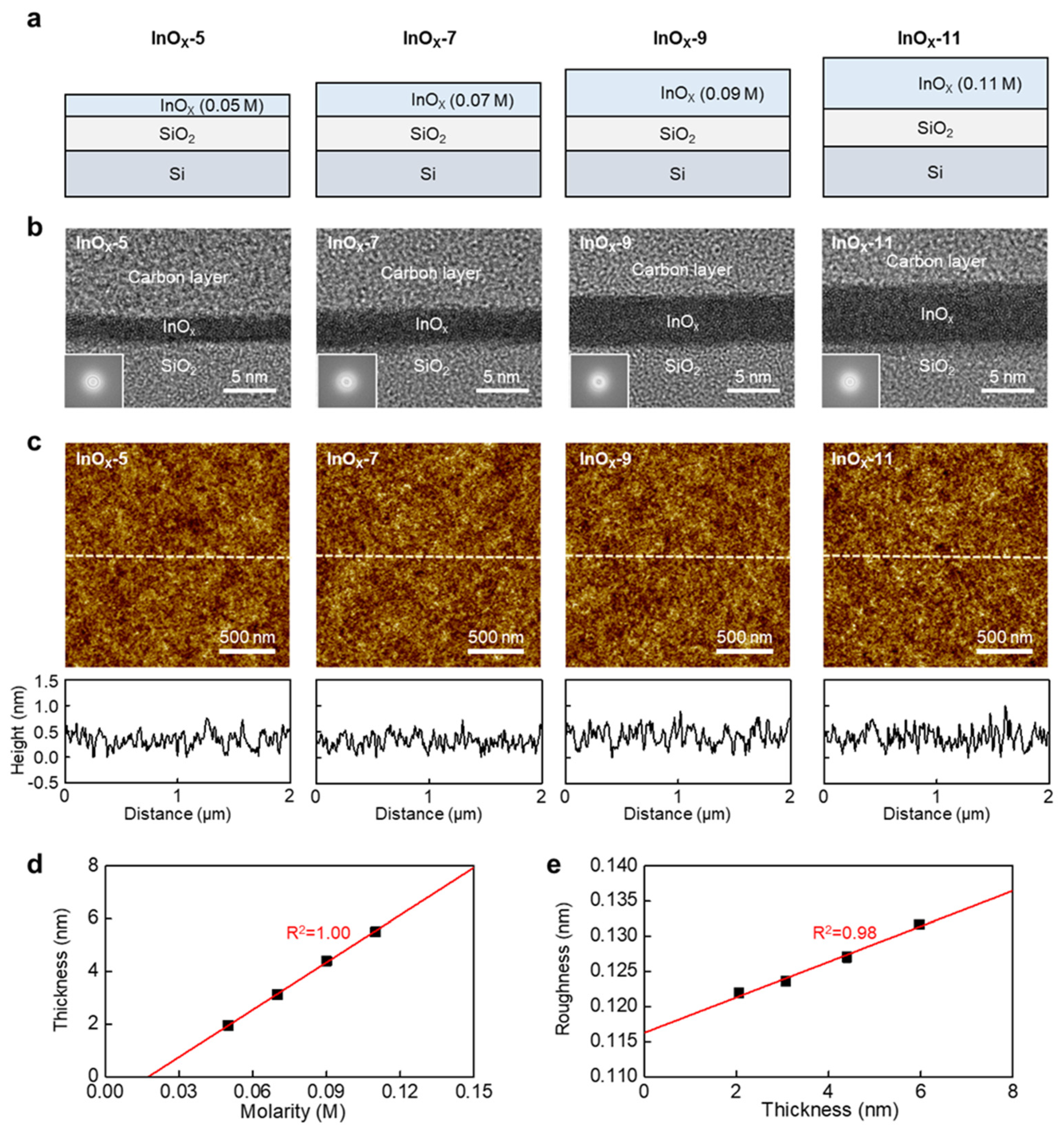
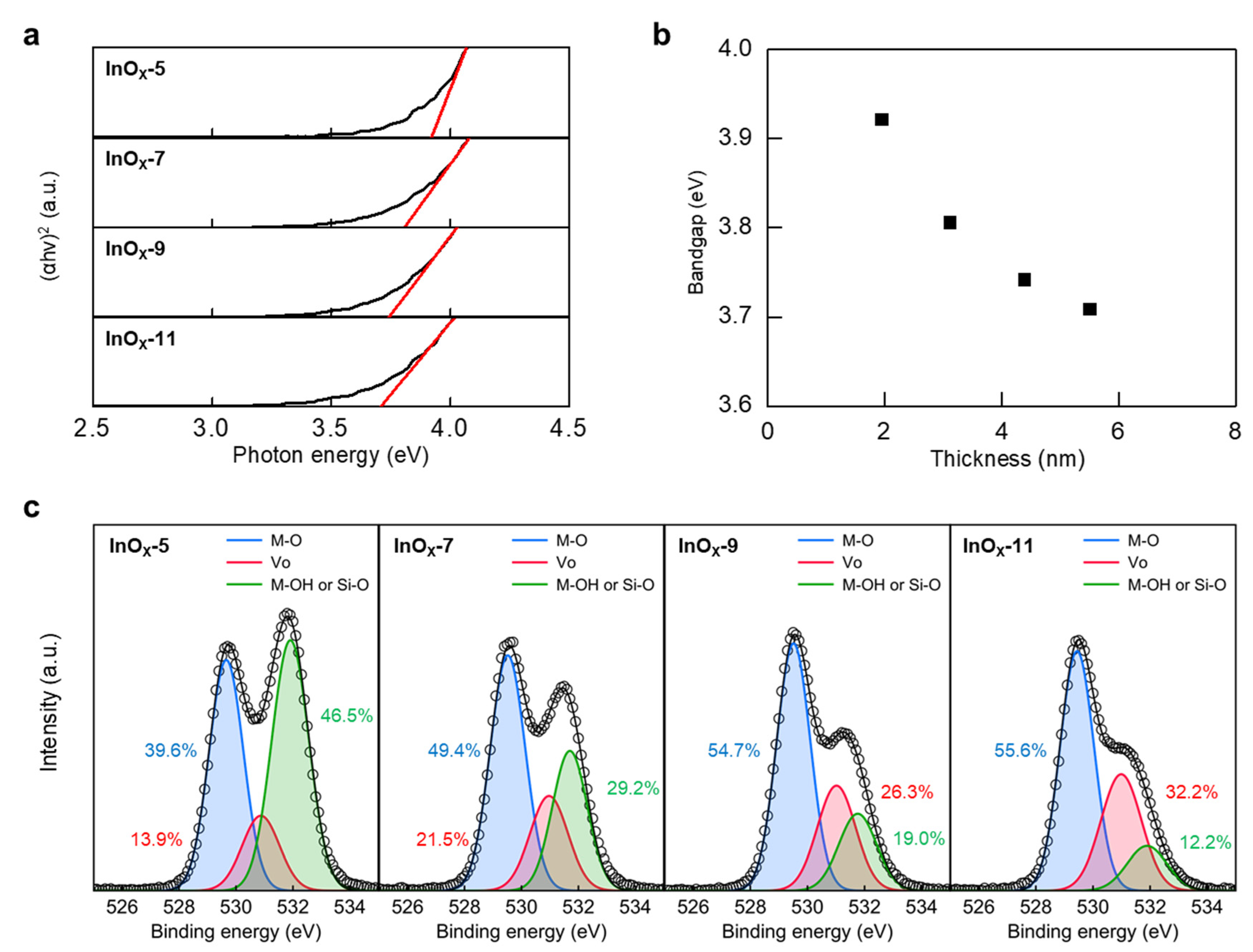
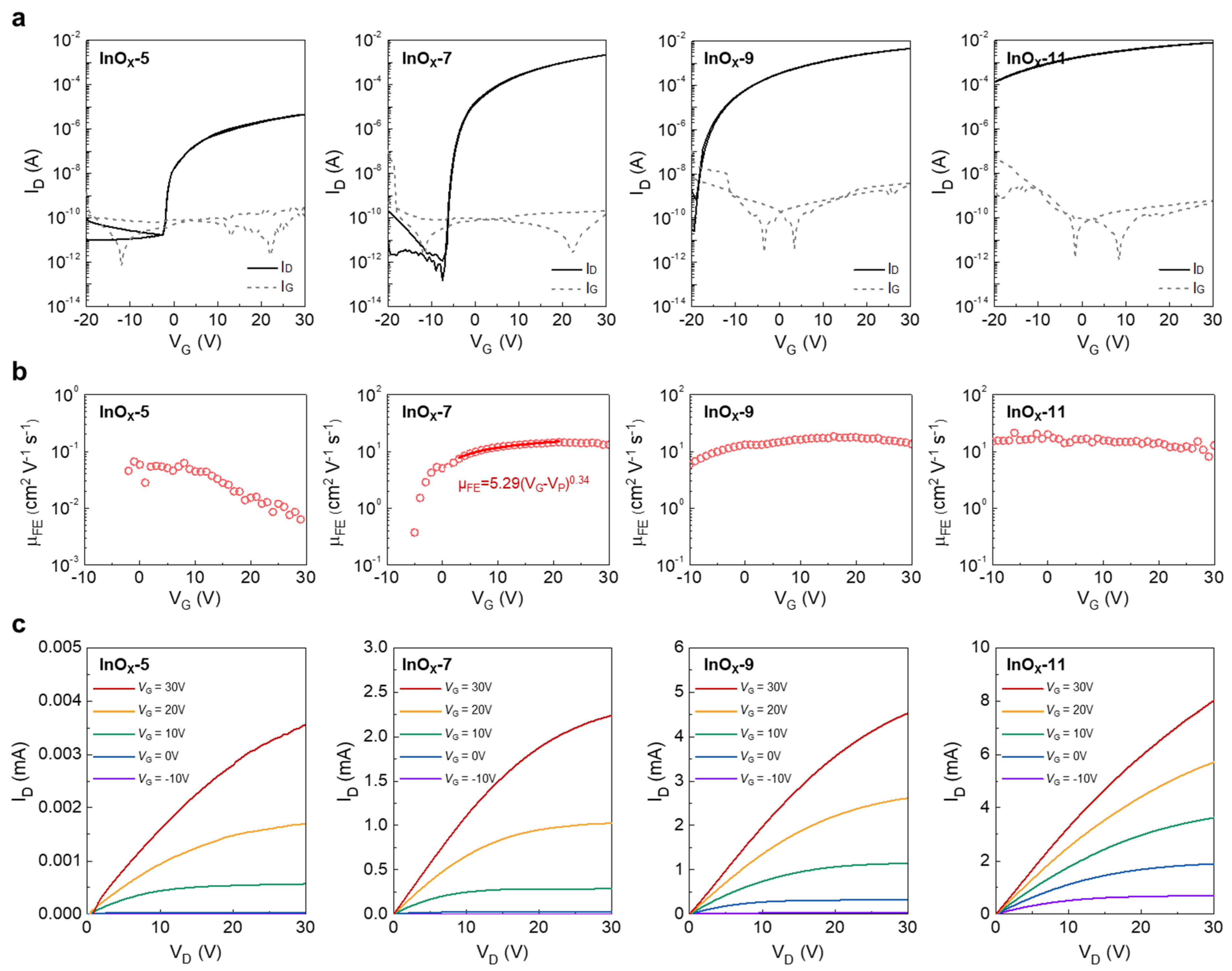
3. Results and Discussion

The physical characteristics of atomically thin InOx semiconductors were investigated. The InOx semiconductors were deposited using solutions with low molarities, namely 0.05, 0.07, 0.09, and 0.11 M, to obtain films with sub-10-nanometer thicknesses, as depicted in Figure 1. All InOx thin films were deposited on Si/SiO2 wafers to enable physical analysis, and film thickness was controlled by fine-tuning the solution molarity, as shown in Figure 2a. As shown in the TEM images of InOx-5, InOx-7, InOx-9, and InOx-11 in Figure 2b, the InOx thickness gradually decreases as the molarity decreases. Interestingly, while binary oxides usually have a polycrystalline or nanocrystalline phase, all InOx films in this study exhibit an amorphous phase, as confirmed in selected area electron diffraction (SAED) patterns, which is favored by industry because it enables the realization of large-area displays and high uniformity and yield (inset of Figure 2b) [18]. In particular, InOx typically crystallizes in a cubic structure even at low annealing temperatures [19]. This unique result is attributed to the supply of water molecules to InOx at the initial stage of film formation during the etching step (Figure S1) [17,20]. The amorphous phase is also confirmed via GIXRD patterns, which agree with the SAED patterns (Figure S2). Element mapping was carried out for O, In, and Si. Element mapping showed that the InOx thickness gradually decreased as molarity increased (Figure S3). AFM images (Figure 2c, top) and the corresponding height profiles (Figure 2c, bottom) of InOx-5, InOx-7, InOx-9, and InOx-11 are shown in Figure 2c to confirm the surface morphology of ultrathin InOx at various solution molarities. The yellow dashed line in the AFM images indicates where the height profiles were measured. All samples show smooth surfaces because the films were deposited via spin coating, which is a desirable method used to form thin and uniform films. The correlations between molarity, thickness, and roughness were demonstrated. Figure 2d,e presents the correlations between molarity and thickness and thickness and roughness, respectively. The average thicknesses of InOx-5, InOx-7, InOx-9, and InOx-11 were 1.95, 3.12, 4.40, and 5.51 nm, respectively. As expected, the thickness linearly increased with the increase in the molarity because molarity indicated the concentration of indium in the solution (Figure 2d). Although the spin coating speed was also one of the methods used to control semiconductor thickness, the controllability of the thickness via this method was poor because the coating speed and thickness did not have linearity. Therefore, the molarity was controlled in this study because it has linearity with thickness. We noted that due to the low viscosity of solution and high spin speed, there was a negligible difference in the thickness of the center and edge regions within the substrate, showing high thickness uniformity. The R-squared (R2) was extracted to examine how well an estimated linear model fit a given dataset. An R2 of 1.00 was obtained for the molarity–thickness plots, implying a very high correlation. The average root-mean-square (RMS) surface roughnesses of InOx-5, InOx-7, InOx-9, and InOx-11 were 0.122, 0.123, 0.125, and 0.132 nm, respectively. The RMS roughness was linearly increased by increasing the semiconductor thickness at the atomic scale and showing a high R2 of 0.98 in the roughness–thickness plot (Figure 2e).
Optical bandgaps (Eg) of InOx with various thicknesses were investigated using a UV–Vis spectrophotometer. The Eg was extracted via the extrapolated linear fit of (αhν)2 versus the photon energy, as shown in Figure 3a. The extracted Eg of InOx-5, InOx-7, InOx-9, and InOx-11 were 3.92, 3.92, 3.90, and 3.88 eV, respectively. The Eg of InOx tended to increase as the thickness became thinner, which was mainly explained by the quantum confinement effect (Figure 3b) [21,22]. Changes in the chemical bonding states of InOx with various solution molarities were also investigated using XPS analysis. Figure 3c shows the O1s spectra of InOx-5, InOx-7, InOx-9, and InOx-11. The oxygen bonding states were analyzed via deconvolution into three Gaussian peaks corresponding to the oxygen species of the metal–oxide (M–O), oxygen vacancy (Vo), and metal–hydroxide (M–OH). The three main Gaussian curves of M–O, Vo, and M–OH were centered at approximately 530.3 ± 0.2, 531.5 ± 0.2, and 532.5 ± 0.2 eV, respectively [23,24,25,26]. We noted that the curve at about 532.5 eV could be interpreted as Si–O [27,28]. Si atoms of SiO2 usually diffused into the oxide semiconductor during the annealing process in metal–oxide TFT fabrications, meaning that Si–O bonding might exist at the interface between the SiO2 dielectric and InOx semiconductor [28]. Here, the ratio of Si–O at the InOx surface gradually increases as the thickness of InOx decreases because InOx thin films are atomically thin with a sub-5-nanometer thickness. In addition, since all processes, except for solution molarity, were identically performed and simultaneously fabricated in the same environment, it is reasonable to interpret the peak at 523.5 eV as Si–O rather than M–OH.
Atomically thin amorphous InOx TFTs with various solution molarities were fabricated to demonstrate their electrical characteristics. Figure 4a shows the transfer characteristics of InOx-5, InOx-7, InOx-9, and InOx-11. To investigate the transfer characteristics, the gate voltage (VG) was varied from −20 to 30 V, while the drain voltage (VD) was fixed at 30 V. The solid and dotted lines in Figure 4a show the drain (ID) and gate currents (IG), respectively. The threshold voltage (VT) was calculated by fitting a straight line to the plot of the square root of ID versus VG in the saturation region (Figure S4). As the thickness of InOx increased, the VT negatively shifted and μFE increased. The large negative shift of VT with increasing molarity originated from an increase in the total number of carriers in the semiconductor. Although the electron concentration was the same, the total number of electrons increased as the semiconductor thickness increased, and channels were formed relatively easily as VG increased. Although InOx-5 had a low off-current level of 10−12 A and a positive VT, which is desirable in circuit design, a very low μFE of InOx-5 might be insufficient to operate the electronic devices [29,30]. On the other hand, InOx-9 and InOx-11 had high on-currents, but their inferior switching characteristics were not suitable for switching transistors in applications such as displays. On the other hand, InOx-7 had a high μFE and Ion/off of 13.95 cm2 V−1 s−1 and 1.42 × 10¹⁰, respectively, meaning that it was considered to be an optimized device with a high electrical performance. The slight difference in IG for each device might have originated from the subtle differences in the thermally grown SiO2 film quality rather than the InOx layer characteristics or fabrication process.
To deduce the charge transport mechanism in the atomically thin InOx TFTs, μFE in relation to VG is shown in Figure 4b. The gradual decrease in μFE with increasing VG in InOx-5 suggested that surface roughness scattering dominated in ultrathin semiconductor-based TFTs [21]. Thus, the fluctuation in potential energy due to surface roughness has a high effect on long-range electron transport. In InOx-7, μFE gradually increased as VG increased, especially showing a power law behavior [17,31,32]. At high VG, the exponent γ extracted through power law fitting was 0.34, indicating that electron transport was based on percolation conduction. An increase in VG led to an increase in electron concentration in the channel, which meant that the Fermi level was closer to the conduction band. As the Fermi level increased, the interference of electronic conduction of the potential barrier became insignificant. As the thickness increased, the bandgap became narrower, and the number of carriers in the semiconductor increased. Therefore, when the same VG was applied, the electron concentration of the channel was relatively high in oxide TFTs, having a thick semiconductor film compared to that of the oxide TFTs with thin semiconductor films. Consequently, the gap between the Fermi level and conduction band minimum was closer in thick semiconductor. Therefore, the potential barrier formed above the conduction band minimum appeared to be relatively low from the perspective of electron [32]. Therefore, as the thickness of InOx increased, the percolation effect in InOx decreased, and the band-like transport became dominant. The extracted γ value in the power law model of InOx-7 was 0.34, and it indicated that the electron transport was governed by the percolation conduction because it was generally understood that the percolation conduction is dominant when γ was close to 0.1 [31]. In several of the studies reported in the literature related to percolation conduction, the γ values were in the range of 0.12 to 0.34, which is comparable to this study [33,34,35,36]. Meanwhile, a negligible change in μFE occurred with an increase in VG in InOx-9 and InOx-11. This result implied that controlling the semiconductor thickness at the atomic scale allowed the effective tuning of electrical characteristics. In addition, it was confirmed that InOx TFTs were saturated in the VDVGVT region by output characteristics, as shown in Figure 4c. In addition, the device-to-device uniformity of optimized TFTs InOx-7 was investigated by measuring 30 devices through the fabrication of three InOx-7 samples (10 devices per sample), as shown in Figure S5. Figure S5a shows the schematic illustration of fabricated TFT arrays and measurement points used for statistical evaluation. As shown in Figure S5b,c, considering that the devices were fabricated through a solution process, the reasonable high device-to-device uniformity was obtained, although the semiconductor thickness was at the atomic scale [17,37]. This result might be attributed to the fact that the InOx used in this study had high film quality with few physical and chemical defects due to the densification and condensation effects incurred via water etchant [17].
The electrical performances of atomically thin InOx TFTs used in this work were benchmarked with recently reported high-performance oxide TFTs, as shown in Figure 5. All of the data presented here were derived from the solution-processed oxide TFTs with SiO2 dielectrics, since mobility overestimation via high-k dielectrics could affect quantitative comparison. The semiconductor materials, processing temperature, and electrical characteristics presented are in Figure 5 and summarized in Table S1. We noted that the operating conditions, such as biased range or value, are not exactly the same for each study, but almost all of them were driven under the similar conditions that could be acceptable in quantitative comparison. TFTs fabricated in this study showed high μFE at a relatively low processing temperature and positive VT (Figure 5a,b). From an industrial perspective, the processing temperature of 300 °C enabled the utilization of flexible polymer substrates and minimized the process risks. Furthermore, it allowed the back-end-of-line fabrication. Thus, it could be considered to be a sufficiently low processing temperature in the display and semiconductor industries [38]. Furthermore, a positive VT was preferred to a negative VT because it was advantageous in circuit design and power consumption [29,30]. As shown in Figure 5c, oxide TFTs used in this work had a superior Ion/off of about 1010 using the high μFE. High Ion/off contributed to the decrease in the leakage current when the transistor was in off state, and the high μFE allowed the lowering of the operating voltage to achieve the specific current required to drive the circuit or emit light. Therefore, the high Ion/off and μFE enabled an improvement in power efficiency. These comparisons imply that the proposed atomically thin amorphous InOx TFTs had considerable suitability as a candidate for use in a unit device in next-generation electronic device applications.
Bias stability is one of the most important factors in the commercial use of electronic devices. In this regard, the bias stress test was carried out to demonstrate the bias stabilities of the optimized atomically thin amorphous oxide TFT InOx-7. To demonstrate the positive bias stress (PBS)-induced instability of the InOx-7, VGs of 10 and 30 V were applied for 3000 s at room temperature, as shown in Figure 6a,b, respectively. A VD of 0 V was applied during PBS tests. After stress, transfer characteristics were measured at a VD of 30 V. Compared to PBS at a VG of 10 V, the PBS at a VG of 30 V experienced a more severe transfer curve shift due to strong gate bias stress. To understand the PBS-induced instability, variations in VT, SS, and µFE with stress time were extracted (Figure 6c). Regardless of the applied VG during PBS, VT shifted positively, while SS did not noticeably change as the stress time increased. In addition, µFE gradually decreased with the positive shift in VT. This result could be interpreted as meaning that the interface traps were not additionally created via bias stress, and the VT shift originated from the electron trapping at the interface and electron injection into the gate dielectric (Figure 6d) [39,40]. For NBS tests, VGs of −10 and −30 V were applied for 3000 s at room temperature, as shown in Figure 6e,f, respectively. The VD of 0 V was applied during the NBS test, and transfer characteristics were measured at VD of 30 V, i.e., the same as the PBS tests. A negative shift in the VT of InOx-7 was observed using the stressed VGs of −10 and −30 V. Interestingly, the change in SS was negligible when the stress VG was −10 V, while it showed a gradual increase with the increasing stress time when the stress VG was −30 V (Figure 6g). These different trends imply that when NBS at a VG of −10 or −30 V was applied to InOx-7, the devices underwent degradation via different mechanisms. The fact that SS did not increase via NBS at a VG of −10 V suggests that the VT shift occurred due to hole trapping and injection rather than the degradation due to defect creation (Mechanism (1) in Figure 6h) [39]. On the other hand, the increase in SS via NBS at a VG of −30 V indicated the formation of acceptor-like defects during NBS. In general, defects at deep levels, such as Vo, in oxide semiconductors are ionized via illumination stress [39,41]. However, the Fermi level approached the valence band maximum via band bending due to the strong negative gate bias; the formation energy of Vo2+ became lower than that of Vo [42]. Two electrons released via the transition from Vo to Vo2+ induced a negative shift in VT. Meanwhile, the Vo2+ migrated to the gate dielectric–semiconductor interface via the negative gate bias, thereby acting as an acceptor-like trap (Mechanism (2) in Figure 6h). Therefore, it was reasonable to estimate that the degradation mechanisms caused by NBS with VG of −10 and −30 V were caused by the hole trapping and injection and Vo ionization, respectively, in solution-processed atomically thin amorphous InOx TFTs.

4. Conclusions

In this study, we demonstrated high-performance solution-processed oxide TFTs with atomically thin InOx semiconductors. Based on the linearity between solution molarity and film thickness, the thickness of InOx was precisely controlled by adjusting the molarity of the solution. As a result, ultrathin and uniform layers of 1.95–5.51 nm were deposited through the solution process. The bandgap of InOx increased as the thickness decreased due to the quantum confinement effect, and, thus, high μFE and Ion/off of 13.95 cm2 V−1 s−1 and 1.42 × 10¹⁰, respectively, were obtained in InOx TFTs at an optimized InOx thickness of 3.12 nm. Furthermore, atomically thin InOx TFTs showed superior positive and negative gate bias stress stabilities. Their degradation mechanisms were also investigated by analyzing the change in the electrical parameters via gate bias stress. The proposed atomically thin InOx TFTs are expected to contribute to the realization of high-performance printed transistors for use in next-generation electronic applications.

Supplementary Materials

The following supporting information can be downloaded via the following link: https://www.mdpi.com/article/10.3390/nano13182568/s1. Figure S1. Proposed chemical reaction mechanism of InOx by water etchant-based photopatterning method. Figure S2. GIXRD spectra of InOx thin films with various solution molarities. Figure S3. In, O, and Si element mappings of (a) InOx-5, (b) InOx-7, (c) InOx-9, and (d) InOx-11 deposited on SiO2 dielectric. Figure S4. I D 1 2 VG curves and linear fitting of (a) InOx-5, (b) InOx-7, (c) InOx-9, and (d) InOx-11. Figure S5. (a) Schematic illustration of fabricated TFT arrays and measurement points (red box) for statistical evaluation. (b) Distribution of VT (top) and μFE (bottom) of three InOx-7 samples. (c) Statistical data of VT (left) and μFE (right) for three InOx-7 samples (10 points per sample). Table S1. Summary of recently reported solution-processed oxide TFTs with SiO2 dielectrics and this work. The data are used in Figure 5.

Author Contributions

Conceptualization, J.-H.P., D.-K.K. and J.-H.B.; methodology, J.-H.P. and W.P.; validation, J.-H.P.; formal analysis, J.F. and J.-H.N.; investigation, D.-K.K., J.-H.P. and J.L.; data curation, J.-H.P. and J.-S.E.; writing—original draft preparation, J.-H.P.; writing—review and editing, D.-K.K. and J.-H.B.; supervision, D.-K.K. and J.-H.B. All authors have read and agreed to the published version of the manuscript.

Funding

This work was supported by a National Research Foundation of Korea (NRF) grant funded by the Korea government (MSIT) (2021R1A2C1011429). This research was also supported by the MSIT (Ministry of Science and ICT), Korea under the Innovative Human Resource Development for Local Intellectualization support program (IITP-2023-RS-2022-00156389), as well as supervised by the IITP (Institute for Information and Communications Technology Planning and Evaluation).

Data Availability Statement

Not applicable.

Conflicts of Interest

The authors declare no conflict of interest.

References

  1. Fortunato, E.; Barquinha, P.; Martins, R. Oxide Semiconductor Thin-Film Transistors: A Review of Recent Advances. Adv. Mater. 2012, 24, 2945–2986. [Google Scholar] [PubMed]
  2. Rim, Y.S. Review of metal oxide semiconductors-based thin-film transistors for point-of-care sensor applications. J. Inf. Disp. 2020, 21, 203–210. [Google Scholar] [CrossRef]
  3. Si, M.; Lin, Z.; Chen, Z.; Sun, X.; Wang, H.; Ye, P.D. Scaled indium oxide transistors fabricated using atomic layer deposition. Nat. Electron. 2022, 5, 164–170. [Google Scholar] [CrossRef]
  4. Fukuda, K. Recent Progress in the Development of Printed Thin-Film Transistors and Circuits with High-Resolution Printing Technology. Adv. Mater. 2017, 29, 1602736. [Google Scholar] [CrossRef] [PubMed]
  5. Park, J.W.; Byung, H.K.; Kim, H.J. A Review of Low-Temperature Solution-Processed Metal Oxide Thin-Film Transistors for Flexible Electronics. Adv. Funct. Mater. 2020, 30, 1904632. [Google Scholar] [CrossRef]
  6. Xu, W.; Li, H.; Xu, J.-B.; Wang, L. Recent Advances of Solution-Processed Metal Oxide Thin-Film Transistors. ACS Appl. Mater. Interfaces 2018, 10, 25878–25901. [Google Scholar] [CrossRef]
  7. Ahn, B.D.; Jeon, H.-J.; Sheng, J.; Park, J.; Park, J.-S. A review on the recent developments of solution processes for oxide thin film transistors. Semicond. Sci. Technol. 2015, 30, 064001. [Google Scholar] [CrossRef]
  8. Hwang, S.; Lee, J.H.; Woo, C.H.; Lee, J.Y.; Cho, H.K. Effect of annealing temperature on the electrical performances of solution-processed InGaZnO thin film transistors. Thin Solid Films. 2011, 519, 5146–5149. [Google Scholar] [CrossRef]
  9. Kim, M.-G.; Kanatzidis, M.G.; Facchetti, A.; Marks, T.J. Low-temperature fabrication of high-performance metal oxide thin-film electronics via combustion processing. Nat. Mater. 2011, 10, 382–388. [Google Scholar] [CrossRef]
  10. Kim, Y.-H.; Heo, J.-S.; Kim, T.-H.; Park, S.; Yoon, M.-H.; Kim, J.; Oh, M.S.; Yi, G.-R.; Noh, Y.-Y.; Park, S.K. Flexible metal-oxide devices made by room-temperature photochemical activation of sol–gel films. Nature 2012, 489, 128–132. [Google Scholar] [CrossRef]
  11. Lee, M.; Jo, J.-W.; Kim, Y.-J.; Choi, S.; Kwon, S.M.; Jeon, S.P.; Facchetti, A.; Kim, Y.-H.; Park, S.K. Corrugated Heterojunction Metal-Oxide Thin-Film Transistors with High Electron Mobility via Vertical Interface Manipulation. Adv. Mater. 2018, 30, 1804120. [Google Scholar] [CrossRef] [PubMed]
  12. Khim, D.; Lin, Y.-H.; Nam, S.; Faber, H.; Tetzner, K.; Li, R.; Zhang, Q.; Li, J.; Zhang, X.; Anthopoulos, T.D. Modulation-Doped In2O3/ZnO Heterojunction Transistors Processed from Solution. Adv. Mater. 2017, 29, 1605837. [Google Scholar] [CrossRef] [PubMed]
  13. Han, S.-Y.; Herman, G.S.; Chang, C.-H. Low-Temperature, High-Performance, Solution-Processed Indium Oxide Thin-Film Transistors. J. Am. Chem. Soc. 2011, 133, 5166–5169. [Google Scholar] [CrossRef] [PubMed]
  14. Hwang, Y.H.; Seo, J.-S.; Yun, J.M.; Park, H.; Yang, S.; Ko Park, S.-H.; Bae, B.-S. An ‘aqueous route’ for the fabrication of low-temperature-processable oxide flexible transparent thin-film transistors on plastic substrates. NPG Asia Mater. 2013, 5, e45. [Google Scholar] [CrossRef]
  15. Si, M.; Hu, Y.; Lin, Z.; Sun, X.; Charnas, A.; Zheng, D.; Lyu, X.; Wang, H.; Cho, K.; Ye, P.D. Why In2O3 Can Make 0.7 nm Atomic Layer Thin Transistors. Nano Lett. 2021, 21, 500–506. [Google Scholar] [CrossRef]
  16. Charnas, A.; Lin, Z.; Zhang, Z.; Ye, P.D. Atomically thin In2O3 field-effect transistors with 1017 current on/off ratio. Appl. Phys. Lett. 2021, 119, 263503. [Google Scholar] [CrossRef]
  17. Kim, D.-K.; Seo, K.-H.; Kwon, D.-H.; Jeon, S.-H.; Hwang, Y.-J.; Wang, Z.; Park, J.; Lee, S.-H.; Jang, J.; Kang, I.M.; et al. Viable strategy to minimize trap states of patterned oxide thin films for both exceptional electrical performance and uniformity in sol–gel processed transistors. Chem. Eng. J. 2022, 441, 135833. [Google Scholar] [CrossRef]
  18. Kamiya, T.; Hosono, H. Material characteristics and applications of transparent amorphous oxide semiconductors. NPG Asia Mater. 2010, 2, 15–22. [Google Scholar] [CrossRef]
  19. Babu, S.H.; Kaleemulla, S.; Rao, N.M.; Krishnamoorthi, C. Indium oxide: A transparent, conducting ferromagnetic semiconductor for spintronic applications. J. Magn. Magn. Mater. 2016, 416, 66–74. [Google Scholar] [CrossRef]
  20. Wang, M.H.; Onai, Y.; Hoshi, Y.; Lei, H.; Kondo, T.; Uchida, T.; Singkarat, S.; Kamwanna, T.; Dangtip, S.; Aukkaravittayapun, S.; et al. Thermal change of amorphous indium tin oxide films sputter-deposited in water vapor atmosphere. Thin Solid Films 2008, 516, 5809–5813. [Google Scholar] [CrossRef]
  21. Isakov, I.; Faber, H.; Mottram, A.D.; Das, S.; Grell, M.; Regoutz, A.; Kilmurray, R.; McLachlan, M.A.; Payne, D.J.; Anthopoulos, T.D. Quantum Confinement and Thickness-Dependent Electron Transport in Solution-Processed In2O3 Transistors. Adv. Electron. Mater. 2020, 6, 2000682. [Google Scholar] [CrossRef]
  22. Kim, D.W.; Kim, H.J.; Lee, C.; Kim, K.; Bae, J.-H.; Kang, I.-M.; Jang, J. Influence of Active Channel Layer Thickness on SnO2 Thin-Film Transistor Performance. Electronics 2021, 10, 200. [Google Scholar] [CrossRef]
  23. Chang, T.-H.; Chang, S.-J.; Chiu, C.J.; Wei, C.-Y.; Juan, Y.-M.; Weng, W.-Y. Bandgap-Engineered in Indium–Gallium–Oxide Ultraviolet Phototransistors. IEEE Photon. Technol. Lett. 2015, 27, 915–918. [Google Scholar] [CrossRef]
  24. Lim, K.-H.; Lee, J.; Huh, J.-E.; Park, J.; Lee, J.-H.; Lee, S.-E.; Kim, Y.S. A systematic study on effects of precursors and solvents for optimization of solution-processed oxide semiconductor thin-film transistors. J. Mater. Chem. C. 2017, 5, 7768–7776. [Google Scholar] [CrossRef]
  25. Choi, J.Y.; Heo, K.; Cho, K.-S.; Hwang, S.W.; Kim, S.; Lee, S.Y. Engineering of band gap states of amorphous SiZnSnO semiconductor as a function of Si doping concentration. Sci. Rep. 2016, 6, 36504. [Google Scholar] [CrossRef]
  26. Huang, G.; Duan, L.; Dong, G.; Zhang, D.; Qiu, Y. High-Mobility Solution-Processed Tin Oxide Thin-Film Transistors with High-κ Alumina Dielectric Working in Enhancement Mode. ACS Appl. Mater. Interfaces 2014, 6, 20786–20794. [Google Scholar] [CrossRef]
  27. Zatsepin, D.A.; Mack, P.; Wright, A.E.; Schmidt, B.; Fitting, H.-J. XPS analysis and valence band structure of a low-dimensional SiO2/Si system after Si+ ion implantation. Phys. Status Solidi A 2011, 208, 1658–1661. [Google Scholar] [CrossRef]
  28. Kim, C.H.; Rim, Y.S.; Kim, H.J. The effect of a zinc–tin-oxide layer used as an etch-stopper layer on the bias stress stability of solution-processed indium–gallium–zinc-oxide thin-film transistors. J. Phys. D Appl. Phys. 2014, 47, 385104. [Google Scholar] [CrossRef]
  29. Sohn, Y.; Moon, G.; Choi, K.; Kim, Y.; Park, K. Effects of TFT mobility variation in the threshold voltage compensation circuit of the OLED display. J. Inf. Disp. 2017, 18, 25–30. [Google Scholar] [CrossRef]
  30. Choi, S.; Park, J.; Hwang, S.-H.; Kim, C.; Kim, Y.-S.; Oh, S.; Baeck, J.H.; Bae, J.U.; Noh, J.; Lee, S.-W.; et al. Excessive Oxygen Peroxide Model-Based Analysis of Positive-Bias-Stress and Negative-Bias-Illumination-Stress Instabilities in Self-Aligned Top-Gate Coplanar In–Ga–Zn–O Thin-Film Transistors. Adv. Electron. Mater. 2022, 8, 2101062. [Google Scholar] [CrossRef]
  31. Lee, S.; Ghaffarzadeh, K.; Nathan, A.; Robertson, J.; Jeon, S.; Kim, C.; Song, I.-H.; Chung, U.-I. Trap-limited and percolation conduction mechanisms in amorphous oxide semiconductor thin film transistors. Appl. Phys. Lett. 2011, 98, 203508. [Google Scholar] [CrossRef]
  32. Lee, S.; Nathan, A. Localized tail state distribution in amorphous oxide transistors deduced from low temperature measurements. Appl. Phys. Lett. 2012, 101, 113502. [Google Scholar] [CrossRef]
  33. Lin, Y.-H.; Faber, H.; Zhao, K.; Wang, Q.; Amassian, A.; McLachlan, M.; Anthopoulos, T.D. High-Performance ZnO Transistors Processed Via an Aqueous Carbon-Free Metal Oxide Precursor Route at Temperatures between 80–180 °C. Adv. Mater. 2013, 25, 4340–4346. [Google Scholar] [CrossRef] [PubMed]
  34. Liang, K.; Wang, Y.; Shao, S.; Luo, M.; Pecunia, V.; Shao, L.; Zhao, J.; Chen, Z.; Mo, L.; Cui, Z. High-performance metal-oxide thin-film transistors based on inkjet-printed self-confined bilayer heterojunction channels. J. Mater. Chem. C. 2019, 7, 6169–6177. [Google Scholar] [CrossRef]
  35. Tiwale, N.; Senanayak, S.P.; Rubio-Lara, J.; Alaverdyan, Y.; Welland, M.E. Optimization of Transistor Characteristics and Charge Transport in Solution Processed ZnO Thin Films Grown from Zinc Neodecanoate. Electron. Mater. Lett. 2019, 15, 702–711. [Google Scholar] [CrossRef]
  36. He, F.; Qin, Y.; Wan, L.; Su, J.; Lin, Z.; Zhang, J.; Chang, J.; Wu, J.; Hao, Y. Metal oxide heterojunctions for high performance solution grown oxide thin film transistors. Appl. Surf. Sci. 2020, 527, 146774. [Google Scholar] [CrossRef]
  37. Kim, D.-K.; Park, J.-I.; Jang, J.; Kang, I.M.; Park, J.; Bae, J.-H. Expeditious and eco-friendly solution-free self-patterning of sol–gel oxide semiconductor thin films. Mater. Des. 2020, 194, 108949. [Google Scholar] [CrossRef]
  38. Datta, S.; Dutta, S.; Grisafe, B.; Smith, J.; Srinivasa, S.; Ye, H. Back-End-of-Line Compatible Transistors for Monolithic 3-D Integration. IEEE Micro 2019, 39, 8–15. [Google Scholar] [CrossRef]
  39. Jeong, J.K. Photo-bias instability of metal oxide thin film transistors for advanced active matrix displays. J. Mater. Res. 2013, 28, 2071–2084. [Google Scholar] [CrossRef]
  40. Kim, D.H.; Choi, S.; Jang, J.; Kang, H.; Kim, D.M.; Choi, S.-J.; Kim, Y.-S.; Oh, S.; Baeck, J.H.; Bae, J.U.; et al. Experimental decomposition of the positive bias temperature stress-induced instability in self-aligned coplanar InGaZnO thin-film transistors and its modeling based on the multiple stretched-exponential functions. J. Soc. Inf. Disp. 2017, 25, 98–107. [Google Scholar] [CrossRef]
  41. Um, J.G.; Mativenga, M.; Jang, J. Mechanism of positive bias stress-assisted recovery in amorphous-indium-gallium-zinc-oxide thin-film transistors from negative bias under illumination stress. Appl. Phys. Lett. 2013, 103, 033501. [Google Scholar] [CrossRef]
  42. Janotti, A.; Van de Walle, C.G. Oxygen vacancies in ZnO. Appl. Phys. Lett. 2005, 87, 122102. [Google Scholar] [CrossRef]
Figure 1. Schematic of the process of fabrication used for atomically thin InOx TFTs.
Nanomaterials 13 02568 g001
Figure 2. (a) Structures, (b) TEM images and corresponding SAED patterns (inset), and (c) AFM images and corresponding height profiles of InOx thin films at various molarities. (d) InOx film thickness versus molarity. (e) RMS roughness of InOx film versus InOx film thickness.
Nanomaterials 13 02568 g002
Figure 3. (a) (αhν)2 versus photon energy, (b) optical bandgap versus thickness, and (c) XPS O 1s spectra of InOx films with various solution molarities.
Nanomaterials 13 02568 g003
Figure 4. (a) Transfer characteristics, (b) field-effect mobility, and (c) output characteristics of InOx TFTs with various InOx thicknesses.
Nanomaterials 13 02568 g004
Figure 5. Benchmarks of (a) μFE versus processing temperature, (b) μFE versus VT, and (c) log(Ion/off) versus μFE. All works used SiO2 dielectric and solution-processed oxide semiconductors to create TFTs.
Nanomaterials 13 02568 g005
Figure 6. PBS with (a) VG = 10 V and (b) VG = 30 V. (c) Change in electrical parameters of InOx TFTs via positive bias stress. (d) PBS-induced degradation mechanism in InOx TFTs. NBS with (e) VG = −10 V and (f) VG = −30 V. (g) Change in electrical parameters of InOx TFTs via positive bias stress. (h) PBS-induced degradation mechanism in InOx TFTs.
Nanomaterials 13 02568 g006
Disclaimer/Publisher’s Note: The statements, opinions and data contained in all publications are solely those of the individual author(s) and contributor(s) and not of MDPI and/or the editor(s). MDPI and/or the editor(s) disclaim responsibility for any injury to people or property resulting from any ideas, methods, instructions or products referred to in the content.

