Article

The Influence of Capping Layers on Tunneling Magnetoresistance and Microstructure in CoFeB/MgO/CoFeB Magnetic Tunnel Junctions upon Annealing

1
Department of Materials Science and Engineering, Korea Advanced Institute of Science and Technology, Daejeon 34141, Republic of Korea
2
Department of Electronic Engineering, Gachon University, Seongnam 13120, Republic of Korea
3
Samsung Advanced Institute of Technology, Samsung Electronics, Suwon 16678, Republic of Korea
4
Department of Semiconductor Systems Engineering, Korea University, Seoul 02481, Republic of Korea
5
Department of Materials Science and Engineering, Korea University, Seoul 02481, Republic of Korea
*
Authors to whom correspondence should be addressed.
Nanomaterials 2023, 13(18), 2591; https://doi.org/10.3390/nano13182591
Submission received: 18 July 2023 / Revised: 13 September 2023 / Accepted: 16 September 2023 / Published: 19 September 2023
(This article belongs to the Special Issue Advanced Spintronic and Electronic Nanomaterials)

Abstract

:
This study investigates the effects of annealing on the tunnel magnetoresistance (TMR) ratio in CoFeB/MgO/CoFeB-based magnetic tunnel junctions (MTJs) with different capping layers and correlates them with microstructural changes. It is found that the capping layer plays an important role in determining the maximum TMR ratio and the corresponding annealing temperature (Tann). For a Pt capping layer, the TMR reaches ~95% at a Tann of 350 °C, then decreases upon a further increase in Tann. A microstructural analysis reveals that the low TMR is due to severe intermixing in the Pt/CoFeB layers. On the other hand, when introducing a Ta capping layer with suppressed diffusion into the CoFeB layer, the TMR continues to increase with Tann up to 400 °C, reaching ~250%. Our findings indicate that the proper selection of a capping layer can increase the annealing temperature of MTJs so that it becomes compatible with the complementary metal-oxide-semiconductor backend process.

1. Introduction

Magnetic tunnel junctions (MTJs) consisting of ferromagnet (FM)/tunnel barrier/FM structures have been studied extensively because they serve as a key element in various spintronic devices, including the read heads of hard disk drives and magnetic random-access memory devices (MRAMs) [1,2,3,4,5]. In MTJs, tunneling electrons are spin-polarized along the magnetization direction so that the tunneling probability increases (decreases) when the magnetizations of the two FMs are aligned in a parallel (antiparallel) configuration. This spin-dependent tunneling can be enhanced by introducing a (001)-oriented crystalline MgO barrier, where the Δ1 Bloch state allows coherent tunneling [6,7,8]. A large tunneling magnetoresistance (TMR) ratio exceeding hundreds of percent as theoretically predicted in crystalline MgO-based MTJs has been experimentally demonstrated [9,10,11,12].
CoFeB is a widely employed FM electrode in sputter-grown MTJs [11,12,13,14,15,16,17,18,19,20] because, first, amorphous CoFeB favors the growth of the MgO close-packed (001) plane on top [12,15], and second, post-annealing causes boron to diffuse out of CoFeB and subsequently crystallize the amorphous CoFeB into CoFe on the MgO (001) texture [19,20]. It is also known that post-annealing at moderate temperatures improves the material and device properties of the MTJs by reducing defects in the MgO tunnel barrier or ferromagnet/MgO interfaces and/or by enhancing the crystallinity of the MgO layer. This leads to an increase in the TMR ratio or the perpendicular magnetic anisotropy (PMA). Therefore, in order to obtain a large TMR ratio in CoFeB/MgO/CoFeB-structured MTJs, it is essential to perform post-annealing at an elevated temperature. However, the annealing temperature (Tann) must not be excessive such that it causes atomic intermixing between the layers, which diminishes the TMR. Furthermore, for MTJs to be used in practical MRAM applications, they must maintain their characteristics at Tann values above 400 °C, the range in which complementary metal-oxide-semiconductor (CMOS) backend integration takes place [21,22,23].
Many studies have examined annealing effects in antiferromagnet/CoFeB/MgO/CoFeB structures and the interfaces therein [9,12,16,19,24,25,26,27,28,29,30,31,32,33,34,35,36,37,38,39,40,41]. For example, the effect of the Ta capping layer has been extensively investigated. Upon annealing, the Ta capping layer effectively absorbs boron atoms from adjacent CoFeB layers, promoting the crystallization of the amorphous CoFeB layer. Consequently, MTJs with a Ta capping layer exhibit enhanced TMR ratios after annealing within a Tann range of 300~500 °C [12,19,28,29,30,31,32,33,34,35]. The W or Hf capping layer demonstrates similar annealing effects in terms of the increased TMR because of the effective B absorption [36,37,38]. On the other hand, there have been few studies of the effects of annealing on Pt/CoFeB layers [39,40] or a Pt/CoFeB/MgO/CoFeB tunnel junction [41], where PMA deteriorates when samples are annealed with Tann exceeding 300 °C. This was attributed to intermixing between the Pt and CoFeB layers. However, previous studies did not investigate the annealing effect on the TMR ratio in MTJs with a Pt capping layer, especially at the Tann representative of the CMOS-compatible backend process.
Furthermore, heavy-metal (e.g., Pt, Ta, W)/ferromagnet bilayers have been extensively investigated because the spin currents generated in the heavy metal exert spin-orbit torque (SOT) on the ferromagnet and control its magnetization direction. SOT is being developed as a novel writing technology for energy-efficient MRAM [42,43,44,45]. Among such heavy elements, Pt is considered an excellent SOT material owing to its low resistivity and relatively large spin Hall angle, offering a distinct advantage in terms of power consumption for SOT-based spintronic devices over other spin-current source materials. Therefore, it is crucial to investigate the annealing effect on the TMR of CoFeB/MgO/CoFeB MTJs with a Pt capping layer compared to the effects on those with other capping layers.
In this study, we investigated the annealing-temperature dependence of TMR in IrMn/CoFeB/MgO/CoFeB MTJs with different heavy-metal capping layers of Pt, Ta, and W and correlated them with microstructural changes. For a Pt capping layer, the TMR reaches its maximum value of ~95% at Tann of 350 °C and is then reduced as Tann is increased further. Microstructural analyses reveal that annealing causes severe interdiffusion between the Pt and CoFeB layers, which is believed to be responsible for the reduced TMR value. Interestingly, when Ta is used as a capping layer, the TMR increases to ~250% and does not deteriorate even at a Tann of 400 °C, meeting the thermal budget requirements of the CMOS backend process. MTJs with a W capping layer also exhibit similar behavior. Microstructural analyses confirm that intermixing is significantly suppressed in the CoFeB/Ta layer. Our study indicates that an appropriate capping layer can enhance the temperature dependence of the TMR in CoFeB/MgO/CoFeB MTJs.

2. Experimental Section

We fabricated MTJs consisting of a Ni81Fe19 (1 nm)/Ir25Mn75 (15 nm)/Co32Fe48B20 (5 nm)/MgO (2 nm)/Co32Fe48B20 (4 nm) structure with different capping layers of Pt, Ta, and W, as illustrated in Figure 1a. The films were deposited on Si/SiOx (200 nm) substrates by magnetron sputtering at room temperature with a base pressure lower than 3.0 × 10⁻⁸ Torr. During the deposition, a magnetic field of 15 mT was applied to induce uniaxial anisotropy of the CoFeB layers. We deposited metal layers with a DC power of 30 W and a working pressure of 3 mTorr and a MgO layer with a RF power of 75 W and a working pressure of 10 mTorr. The aforementioned thickness of each layer is a nominal value calculated from the deposition rate of the layer, which was measured using a surface profiler (α-step) and an atomic force microscope. A thin NiFe layer was introduced underneath the IrMn layer to promote the exchange bias of the IrMn/CoFeB bilayer. After the film deposition process, we defined a dumbbell-shaped bottom electrode using photolithography and Ar ion milling techniques. The width of the bottom electrode is 10 μm. Then, pillar-shaped MTJs with a diameter of 5 μm were patterned by etching the top electrode and MgO tunnel barrier and in situ passivating a RF-deposited 70 nm thick SiOx layer to electrically disconnect the bottom and top electrodes. Finally, the top electrode was formed by the deposition of a Cr (5 nm)/Au (100 nm) layer and subsequent lift-off process. Figure 1b presents a scanning electron microscope image of the MTJ device. After the fabrication of the device, MTJs were annealed at different temperatures (Tann) ranging from 250 °C to 450 °C for 40 min in a vacuum condition. Here, the maximum Tann of 450 °C was chosen by considering the thermal budget of the CMOS backend process. To establish exchange coupling at the IrMn/CoFeB interface, the annealing was conducted under a magnetic field of 100 mT, which is sufficient to saturate the magnetization of the CoFeB layer. The tunneling resistance was measured using a four-point geometry method with a constant reading current to apply a bias voltage of 10 mV at room temperature while sweeping the in-plane magnetic fields (Bin). The microstructures of the samples were analyzed through high-resolution scanning transmission electron microscopy (HR-STEM), energy dispersive X-ray spectroscopy (EDS), and X-ray diffraction (XRD).

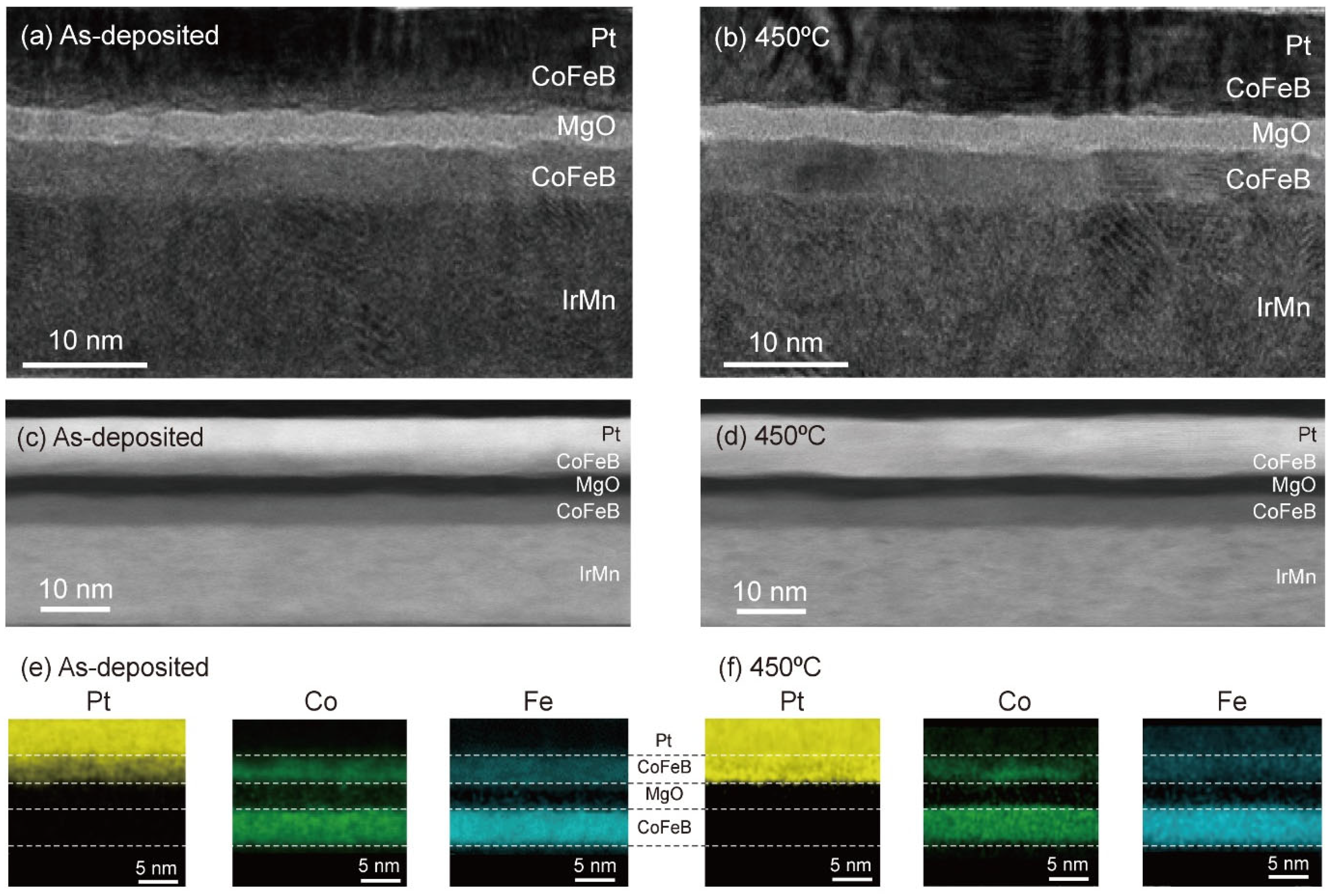
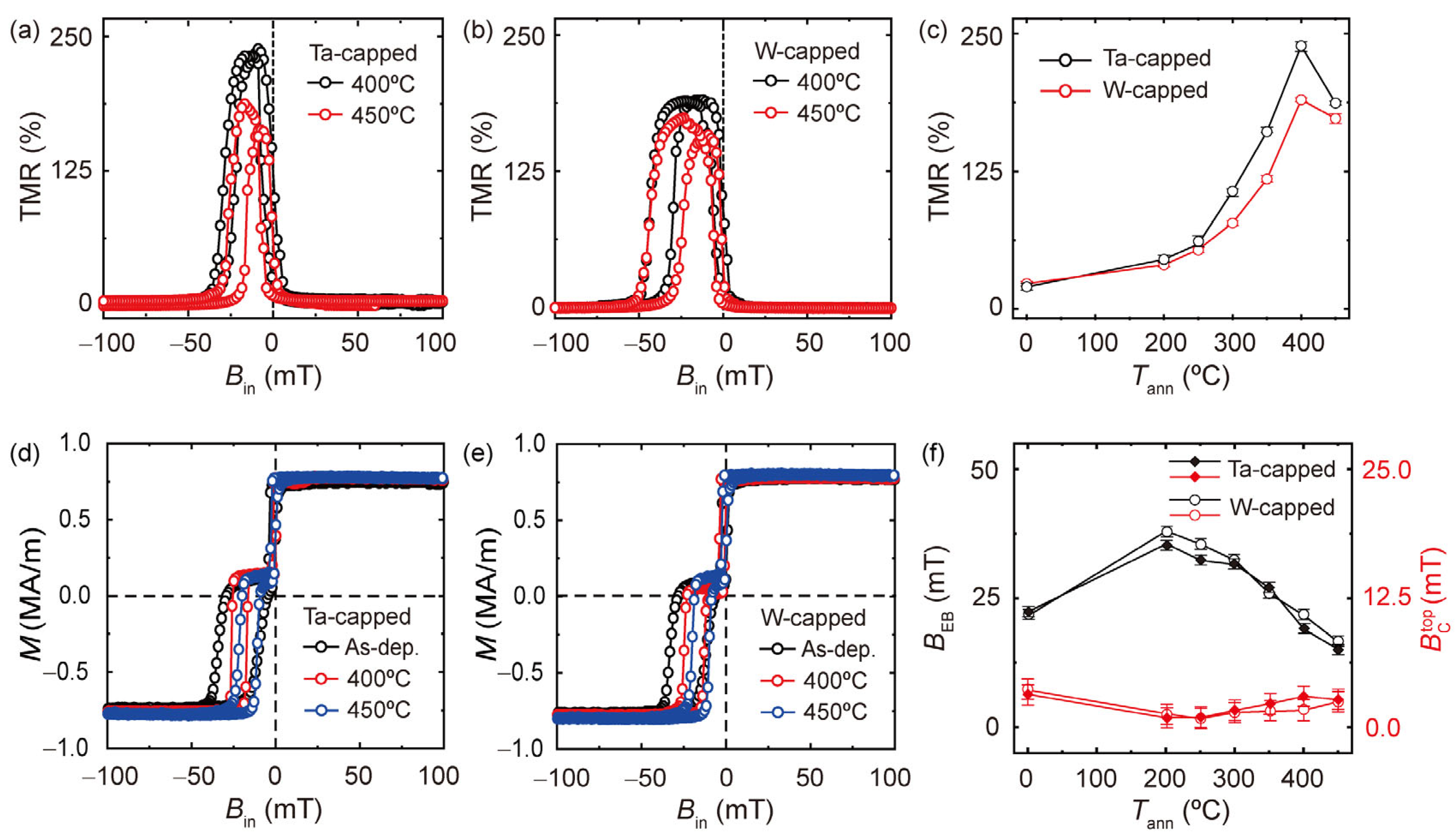
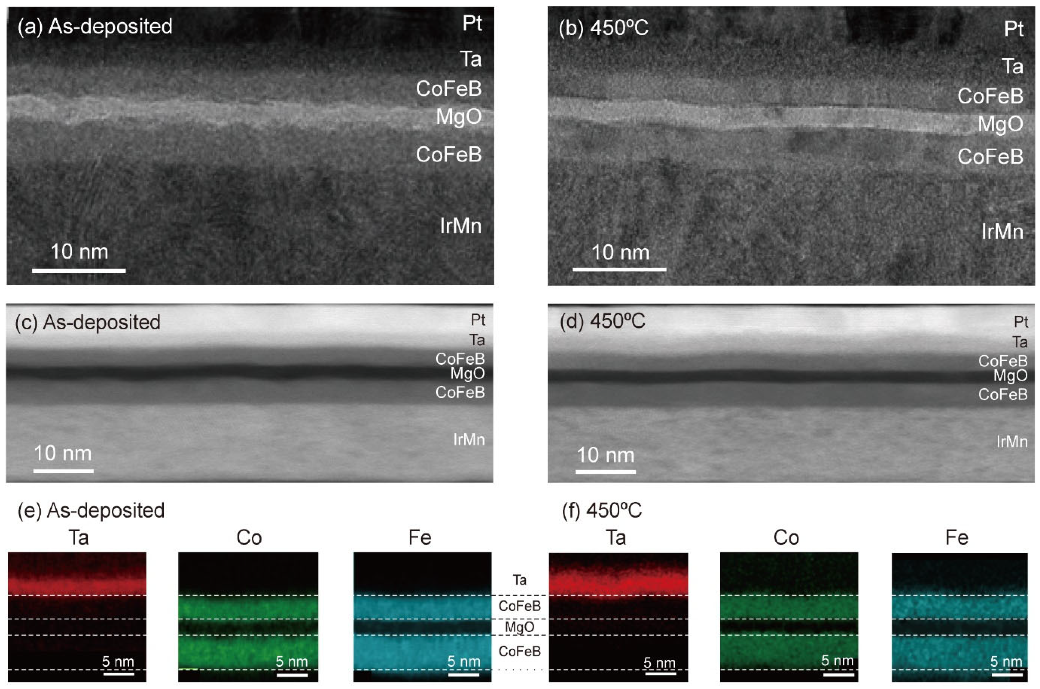
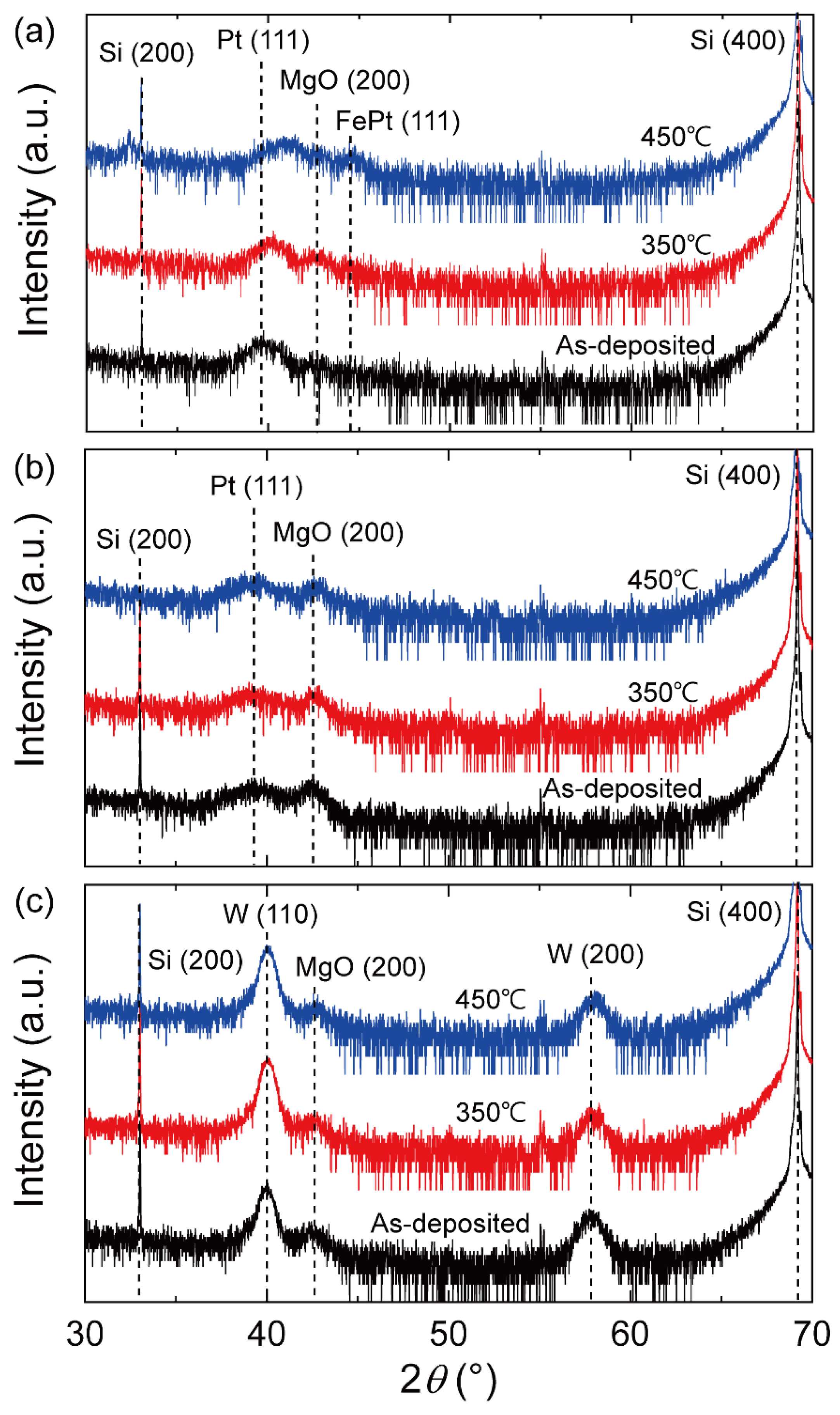
3. Results and Discussion

First, we investigated the annealing effect on the TMR of an MTJ with a Pt (5 nm) capping layer. Figure 1c presents the TMR ratio versus the Bin curves measured for as-deposited and annealed samples at different Tann. Here, the TMR ratio is defined as TMR (%) = [ R T (Bin) −   R T (Bin = 100 mT)]/[ R T (Bin = 100 mT)], where R T is the tunnel resistance of the sample. Note that the magnetization directions of the two CoFeB layers are aligned in a parallel manner when Bin = 100 mT. The TMR curves show a clear distinction between low and high resistance states for the samples for which Tann is below 350 °C, corresponding to the parallel and antiparallel alignment of the top and bottom magnetizations. However, it is severely modified for the sample with Tann equal to 450 °C. Figure 1d shows the TMR as a function of Tann when it ranges from 200 °C to 450 °C. This finding demonstrates two notable points. First, the TMR ratio of the MTJ with the Pt capping layer can only reach ~95% at Tann = 350 °C, much lower than that of typical MgO-based MTJs [12]. Second, the TMR decreases drastically when Tann exceeds 350 °C, which may be related to the modified TMR curve.
We also measured the magnetization curves of MTJs annealed at different Tann by means of vibrating sample magnetometry. Figure 1e shows two hysteresis curves, one centered at Bin = 0 and the other centered at Bin < 0. The former (latter) corresponds to the magnetization of the top magnetically free (bottom exchange-biased) CoFeB layer. Notably, the hysteresis curve of the MTJ with Tann = 450 °C is quite different from those of the other samples, a finding consistent with the TMR curve. Figure 1f shows the extracted exchange-bias field (BEB) of the bottom CoFeB layer and coercivity ( B C top ) of the top CoFeB layer as a function of Tann. Here, BEB initially increases upon annealing at a Tann of 200 °C, after which it gradually decreases upon a further increase in Tann. We can understand the decrease in BEB at a higher Tann in terms of the diffusion of Mn from the antiferromagnet IrMn layer [25,26,27]. The behavior of BEB with Tann is not similar to that of the TMR, and the magnitude of BEB still shows a finite value even after annealing at a Tann of 450 °C, suggesting that the decrease in BEB is not the main cause of the reduction in the TMR ratio at a high Tann. On the other hand, the B C top shows different behavior; the values remain unchanged for both the as-deposited and the annealed samples with Tann values up to 350 °C. However, it increases drastically upon annealing when Tann exceeds 400 °C, with the magnitude becoming ~24 mT, which is more than 10 times greater than those of the samples with lower Tanns. It was also found that the magnetization of the top CoFeB layer decreases slightly after annealing at a Tann of 450 °C. This, together with the large increase in B C top , which causes the antiparallel magnetic alignment to be less pronounced, may be responsible for the reduced TMR ratio.
To understand the Tann dependence of the magnetic properties of the top CoFeB layer and the associated TMR ratio, we conducted microstructural analyses using cross-sectional STEM and EDS. Figure 2a,b correspondingly show bright-field STEM images of the as-deposited sample and its annealed counterpart when Tann = 450 °C. Both images show clear interfaces of the IrMn/bottom CoFeB/MgO/top CoFeB layers. However, we cannot clearly distinguish the interface between the top CoFeB and Pt layers in either film. To clarify the interface quality, we also investigated high-angle annular dark-field (HAADF) images, in which the contrast is correlated with the atomic number. Figure 2c,d present HAADF-STEM images of the as-deposited and annealed films, respectively. The as-deposited film exhibits a contrast difference, albeit weak, between the top CoFeB and Pt layers. However, the annealed film at a Tann of 450 °C shows no contrast difference between the layers. This indicates significant atomic intermixing between the CoFeB/Pt layers.
To assess this intermixing, we construct element mapping images by EDS. Figure 2e,f show images of the as-deposited and annealed films, respectively. Here, yellow, green, and blue represent Pt, Co, and Fe atoms, respectively. It is observed that yellow appears within the top CoFeB layer, even in the as-deposited sample (Figure 2e), indicating that a nonnegligible amount of Pt diffused into the top CoFeB layer during the deposition of the films. The yellow contrast in the top CoFeB layer becomes significantly stronger in Figure 2f, showing that more Pt atoms diffused into the top CoFeB layer by annealing. Note that the contrast of the Co and Fe atoms is not noticeably changed by annealing. We consider Pt diffusion to be the main cause of the reduced TMR. The alloy formation of the diffused Pt with CoFeB can explain the annealing-induced changes in the magnetic properties: an increase in B C top and a decrease in the magnetization of the top CoFeB layer. In addition to increasing B C top , which makes it difficult to distinguish between parallel and antiparallel magnetization states, Pt diffusion may cause other mechanisms that, in turn, decrease the TMR. One may modify the band structure of CoFeB by adding nonmagnetic Pt, reducing the spin polarization value of the CoFeB layer [46]. Another is that Pt with a face-centered cubic (fcc) structure may prevent CoFeB from being epitaxially matched with the body-centered cubic (bcc) MgO (001) structure, reducing the degree of coherent tunneling [39]. Note that the diffusion of Pt into CoFeB must be suppressed in order to utilize Pt as a spin current source in SOT-based spintronic devices. The interdiffusion within the Pt/CoFeB layers can be mitigated by employing rapid thermal annealing (RTA), which reduces the annealing time [47], and by introducing an insertion layer between the Pt and CoFeB layers. The insertion layer must serve as a diffusion barrier while also enabling the transfer of the spin current generated in the Pt layer to the CoFeB layer without a significant loss [28,31,48].
Next, we examine other capping layers of Ta or W that were introduced between the CoFeB and Pt layers while keeping the remaining layers the same. The layer structure is Ni81Fe19 (1 nm)/Ir25Mn75 (15 nm)/Co32Fe48B20 (5 nm)/MgO (2 nm)/Co32Fe48B20 (4 nm)/W or Ta (5 nm)/Pt (5 nm). Hereafter, we refer to the MTJs with a Ta (W) capping layer as Ta-(W-)-capped MTJs. Figure 3a,b show the TMR curves measured at Tann of 400 °C and 450 °C for the Ta- and W-capped MTJs, respectively. Note that Ta and W are extensively utilized as spin-current sources, akin to Pt in SOT-based devices [42,43,49,50]. Unlike the MTJ with a Pt capping layer, the TMR curves of these samples retain their shape with well-defined parallel and antiparallel magnetization states, even after annealing at 450 °C. Figure 3c presents the TMR value as a function of Tann when it ranges from 200 °C to 450 °C, demonstrating a significant improvement in the TMR ratio and the corresponding Tann dependence compared to the Pt-capped MTJs. The maximum TMR ratios become 250% and 190% for the Ta- and W-capped MTJs, respectively. Moreover, Tann leading to the maximum TMR increases to 400 °C for both samples. The slight decrease in the TMR ratio at Tann = 450 °C may be due to Mn diffusion from the bottom IrMn layer at a high Tann [25,26,27]. Figure 3d,e show the magnetization curves of the Ta- and W-capped MTJs films, respectively, with different Tanns of 400 °C and 450 °C. Unlike the sample with a Pt capping layer (Figure 1d), these samples exhibit two clearly distinguished hysteresis loops for all Tanns. Figure 3f shows the extracted BEB of the bottom CoFeB and B C top as a function of Tann. The BEB behavior with regard to the Tann of the samples with the Ta and W capping layers is very similar to that of the Pt sample; BEB initially increases upon annealing at a Tann of 200 °C, followed by a gradual decrease with a further increase in Tann. This result confirms that the change in BEB with Tann is not the main cause of the Tann-dependent TMR. On the other hand, the B C top values do not significantly change for the two samples over the entire Tann range up to 450 °C. This is in stark contrast to the Pt sample (Figure 1e). In addition, the magnetizations of the top CoFeB layer of the W- and Ta-capped samples remain unchanged after annealing at a Tann of 450 °C. These results demonstrate that the magnetic properties of the top CoFeB with the Ta or W capping layer are robust to the annealing at a Tann of up to 450 °C, possibly because of the suppressed atomic diffusion. This is in line with the enhancement of the Tann dependence of the TMR.
Additionally, we investigated the microstructures of Ta-capped MTJ films upon annealing using cross-sectional STEM and EDS. Figure 4a,b show bright-field STEM images of as-deposited and annealed (Tann = 450 °C) films, respectively. Both images reveal well-defined layers and sharp interfaces, including the top CoFeB/Ta layers. The HAADF-STEM images as shown in Figure 4c,d exhibit a clear contrast difference for all layers, confirming that the top CoFeB/Ta layer structure is maintained after annealing at Tann = 450 °C. Figure 4e,f show EDS element mapping images of the as-deposited and annealed films, respectively. Here, red, green, and blue represent Ta, Co, and Fe atoms, respectively. No red color is observed on the top CoFeB layer, indicating that the diffusion of Ta atoms into the top CoFeB layer after annealing at 450 °C was suppressed. This result is in stark contrast to that of the Pt-capped MTJ shown in Figure 2. On the other hand, the green and blue contrasts corresponding to Co and Fe atoms did not change significantly after annealing, similar to the Pt-capped MTJs. The W capping layer shows diffusion behavior similar to that of the Ta layer (Supplementary Information S1). Here, the Pt capping layer more easily intermixes with CoFeB than the Ta or W capping layer, possibly because of the greater solubility of Pt in Co or Fe compared to W or Ta in Co or Fe [51,52,53,54,55,56]. Furthermore, X-ray photoemission spectroscopy measurements reveal that the Ta layer acts as an effective boron absorber during the annealing process, thereby facilitating the crystallization of the CoFeB layer (Supplementary Information S2). These results indicate that the Ta capping layer effectively serves as an appropriate capping layer that suppresses atomic diffusion during the annealing process, consequently enhancing the Tann dependence of the TMR and satisfying the thermal budget requirement of the CMOS backend process.
We also examined microstructural changes upon annealing using the high-resolution θ–2θ XRD measurements. Note that we used thicker MgO (10 nm) and top CoFeB (10 nm) layers than those in the MTJ devices to enhance the XRD signal. Figure 5a shows the XRD spectra of the Pt samples with different Tanns of 350 and 450 °C. It was found that the MgO (200) peak appears after annealing with Tann = 350 °C and that the corresponding intensity decreases at Tann = 450 °C, while the FePt (111) peak appears with 2θ = 44.21° [57]. This result provides the microstructural origins of the significant reduction in the TMR ratio at a high Tann: the degradation of the MgO (001) crystal structure and the formation of a second phase of FePt caused by the diffusion of Pt atoms. On the other hand, Figure 5b,c show the XRD measurement results of the Ta and W samples, where the MgO (200) peaks remain unchanged and no additional peak emerges after annealing at Tann = 450 °C. This again confirms that interdiffusion in the Ta and W samples is significantly suppressed even at a Tann of 450 °C. These results are consistent with the enhanced temperature dependence of the TMR ratio of the Ta- and W-capped MTJs.

4. Conclusions

In this study, we investigated the annealing effect on TMR in IrMn/CoFeB/MgO/CoFeB MTJs with different heavy-metal capping layers. For an MTJ with a Pt capping layer, the TMR reaches a maximum value of ~95% with Tann = 350 °C, decreasing drastically when Tann is increased further. With microstructural analyses using STEM and EDS, we attributed this low TMR to significant intermixing between the Pt and top CoFeB layers. This suggests that in order for Pt to be used as a SOT material, the property degradation after annealing at elevated temperatures must be overcome. Unlike the Pt capping layer, when introducing Ta and W capping layers with suppressed diffusion into the top CoFeB, the TMR ratio and corresponding temperature dependence significantly improved, showing a maximum TMR of ~250% at Tann = 400 °C. Our study highlights the importance of the capping layer, which can significantly affect the MTJ device performance capabilities, suggesting that a proper capping layer will enhance the temperature dependence of the TMR so that applicability to the CMOS backend process can be realized.

Supplementary Materials

The following supporting information can be downloaded at https://www.mdpi.com/article/10.3390/nano13182591/s1. Supplementary Information S1. The diffusion of the W capping layer. Supplementary Information S2. The diffusion of B atoms and crystallization of the CoFeB layers

Author Contributions

Conceptualization, G.K., S.L. (Soogil Lee) and B.-G.P.; investigation, G.K., S.L. (Sanghwa Lee), B.S., D.L. and B.-K.L.; resources, G.K., J.S.L., M.H.L. and Y.K.K.; supervision, S.L. (Soogil Lee) and B.-G.P.; writing—original draft, G.K.; writing—review and editing, G.K, S.L. (Soogil Lee), Y.K.K. and B.-G.P. All authors have read and agreed to the published version of the manuscript.

Funding

This research was funded by the National Research Foundation of Korea (NRF-2022M3H4A1A04096339 and RS-2023-00261042).

Data Availability Statement

Data are available from the correspondence author.

Conflicts of Interest

The authors declare no conflict of interest.

References

  1. Zhu, J.-G.; Park, C. Magnetic tunnel junctions. Mater Today 2006, 9, 36–45. [Google Scholar] [CrossRef]
  2. Yuasa, S.; Fukushima, A.; Yakushiji, K.; Nozaki, T.; Konoto, M.; Maehara, H.; Kubota, H.; Taniguchi, T.; Arai, H.; Imamura, H.; et al. Future prospects of MRAM technologies. In Proceedings of the 2013 IEEE International Electron Devices Meeting, Washington, DC, USA, 9–11 December 2013; pp. 3.1.1–3.1.4. [Google Scholar] [CrossRef]
  3. Hirohata, A.; Yamada, K.; Nakatani, Y.; Prejbeanu, I.-L.; Diény, B.; Pirro, P.; Hillebrands, B. Review on spintronics: Principles and device applications. J. Magn. Magn. Mater. 2020, 509, 166711. [Google Scholar] [CrossRef]
  4. Dieny, B.; Prejbeanu, I.L.; Garello, K.; Gambardella, P.; Freitas, P.; Lehndorff, R.; Raberg, W.; Ebels, U.; Demokritov, S.O.; Akerman, J.; et al. Opportunities and challenges for spintronics in the microelectronics industry. Nat. Electron. 2020, 3, 446–459. [Google Scholar] [CrossRef]
  5. Yuasa, S.; Djayaprawira, D.D. Giant tunnel magnetoresistance in magnetic tunnel junctions with a crystalline MgO(001) barrier. J. Phys. D Appl. Phys. 2007, 40, R337–R354. [Google Scholar] [CrossRef]
  6. Butler, W.H.; Zhang, X.-G.; Schulthess, T.C.; MacLaren, J.M. Spin-dependent tunneling conductance of Fe/MgO/Fe sandwiches. Phys. Rev. B 2001, 63, 054416. [Google Scholar] [CrossRef]
  7. Mathon, J.; Umerski, A. Theory of tunneling magnetoresistance of an epitaxial Fe/MgO/Fe(001) junction. Phys. Rev. B. 2001, 63, 200403. [Google Scholar] [CrossRef]
  8. Zhang, X.-G.; Butler, W.H. Large magnetoresistance in bcc Co/MgO/Co and FeCo/MgO/FeCo tunnel junctions. Phys. Rev. B 2004, 70, 172407. [Google Scholar] [CrossRef]
  9. Parkin, S.S.P.; Kaiser, C.; Panchula, A.; Rice, P.M.; Hughes, B.; Samant, M.; Yang, S.-H. Giant tunnelling magnetoresistance at room temperature with MgO (100) tunnel barriers. Nat. Mater. 2004, 3, 862–867. [Google Scholar] [CrossRef]
  10. Yuasa, S.; Nagahama, T.; Fukushima, A.; Suzuki, Y.; Ando, K. Giant room-temperature magnetoresistance in single-crystal Fe/MgO/Fe magnetic tunnel junctions. Nat. Mater. 2004, 3, 868–871. [Google Scholar] [CrossRef]
  11. Hayakawa, J.; Ikeda, S.; Matsukura, F.; Takahashi, H.; Ohno, H. Dependence of Giant Tunnel Magnetoresistance of Sputtered CoFeB/MgO/CoFeB Magnetic Tunnel Junctions on MgO Barrier Thickness and Annealing Temperature. Jpn. J. Appl. Phys. 2005, 4, L587–L589. [Google Scholar] [CrossRef]
  12. Djayaprawira, D.D.; Tsunekawa, K.; Nagai, M.; Maehara, H.; Yamagata, S.; Watanabe, N.; Yuasa, S.; Suzuki, Y.; Ando, K. 230% room-temperature magnetoresistance in CoFeB/MgO/CoFeB magnetic tunnel junctions. Appl. Phys. Lett. 2005, 86, 092502. [Google Scholar] [CrossRef]
  13. Yuasa, S.; Suzuki, Y.; Katayama, T.; Ando, K. Characterization of growth and crystallization processes in CoFeB∕MgO∕CoFeB magnetic tunnel junction structure by reflective high-energy electron diffraction. Appl. Phys. Lett. 2005, 87, 242503. [Google Scholar] [CrossRef]
  14. Ikeda, S.; Hayakawa, J.; Lee, Y.M.; Tanikawa, T.; Matsukura, F.; Ohno, H. Tunnel magnetoresistance in MgO-barrier tunnel junctions with bcc-CoFe(B) and fcc-CoFe free layers. J. Appl. Phys. 2006, 99, 08A907. [Google Scholar] [CrossRef]
  15. Bae, J.Y.; Lim, W.C.; Kim, H.J.; Lee, T.D.; Kim, K.W.; Kim, T.W. Compositional change of MgO barrier and interface in CoFeB∕MgO∕CoFeB tunnel junction after annealing. J. Appl. Phys. 2006, 99, 08T316. [Google Scholar] [CrossRef]
  16. Read, J.C.; Mather, P.G.; Buhrman, R.A. X-ray photoemission study of CoFeB/MgO thin film bilayers. Appl. Phys. Lett. 2007, 90, 132503. [Google Scholar] [CrossRef]
  17. Mizuguchi, M.; Suzuki, Y.; Nagahama, T.; Yuasa, S. In situ scanning tunneling microscopy observations of polycrystalline MgO(001) tunneling barriers grown on amorphous CoFeB electrode. Appl. Phys. Lett. 2007, 90, 012507. [Google Scholar] [CrossRef]
  18. Cha, J.J.; Read, J.C.; Buhrman, R.A.; Muller, D.A. Spatially resolved electron energy-loss spectroscopy of electron-beam grown and sputtered CoFeB∕MgO∕CoFeB magnetic tunnel junctions. Appl. Phys. Lett. 2007, 90, 062516. [Google Scholar] [CrossRef]
  19. Ikeda, S.; Hayakawa, J.; Ashizawa, Y.; Lee, Y.M.; Miura, K.; Hasegawa, H.; Tsunoda, M.; Matsukura, F.; Ohno, H. Tunnel magnetoresistance of 604% at 300K by suppression of Ta diffusion in CoFeB∕MgO∕CoFeB pseudo-spin-valves annealed at high temperature. Appl. Phys. Lett. 2008, 93, 082508. [Google Scholar] [CrossRef]
  20. Ikeda, S.; Miura, K.; Yamamoto, H.; Mizunuma, K.; Gan, H.D.; Endo, M.; Kanai, S.; Hayakawa, J.; Matsukura, F.; Ohno, H. A perpendicular-anisotropy CoFeB–MgO magnetic tunnel junction. Nat. Mater. 2010, 9, 721–724. [Google Scholar] [CrossRef]
  21. Cardoso, S.; Freitas, P.P.; de Jesus, C.; Soares, J.C. High thermal stability tunnel junctions. J. Appl. Phys. 2000, 87, 6058–6060. [Google Scholar] [CrossRef]
  22. Yamane, K.; Higo, Y.; Uchida, H.; Nanba, Y.; Sasaki, S.; Ohmori, H.; Bessho, K.; Hosomi, M. Spin Torque Switching of Perpendicularly Magnetized CoFeB-Based Tunnel Junctions With High Thermal Tolerance. IEEE Trans. Magn. 2013, 49, 4335–4338. [Google Scholar] [CrossRef]
  23. Thomas, L.; Jan, G.; Zhu, J.; Liu, H.; Lee, Y.-J.; Le, S.; Tong, R.-Y.; Pi, K.; Wang, Y.-J.; Shen, D.; et al. Perpendicular spin transfer torque magnetic random access memories with high spin torque efficiency and thermal stability for embedded applications. J. Appl. Phys. 2014, 115, 172615. [Google Scholar] [CrossRef]
  24. You, C.Y.; Ohkubo, T.; Takahashi, Y.K.; Hono, K. Boron segregation in crystallized MgO/amorphous-Co40Fe40B20 thin films. J. Appl. Phys. 2008, 104, 033517. [Google Scholar] [CrossRef]
  25. Lee, J.H.; Kim, S.J.; Yoon, C.S.; Kim, C.K.; Park, B.G.; Lee, T.D. Thermal stability of the exchanged biased CoFe/IrMn electrode for the magnetic tunnel junction as a function of CoFe thickness. J. Appl. Phys. 2002, 92, 6241–6244. [Google Scholar] [CrossRef]
  26. Lee, Y.M.; Hayakawa, J.; Ikeda, S.; Matsukura, F.; Ohno, H. Giant tunnel magnetoresistance and high annealing stability in CoFeB∕MgO∕CoFeB magnetic tunnel junctions with synthetic pinned layer. Appl. Phys. Lett. 2006, 89, 042506. [Google Scholar] [CrossRef]
  27. Wang, Y.; Zeng, Z.M.; Han, X.F.; Zhang, X.G.; Sun, X.C.; Zhang, Z. Temperature-dependent Mn-diffusion modes in CoFeB- and CoFe-based magnetic tunnel junctions: Electron-microscopy studies. Phys. Rev. B 2007, 75, 214424. [Google Scholar] [CrossRef]
  28. Miyajima, T.; Ibusuki, T.; Umehara, S.; Sato, M.; Eguchi, S.; Tsukada, M.; Kataoka, Y. Transmission electron microscopy study on the crystallization and boron distribution of CoFeB/MgO/CoFeB magnetic tunnel junctions with various capping layers. Appl. Phys. Lett. 2009, 94, 122501. [Google Scholar] [CrossRef]
  29. Pong, P.W.T.; Egelhoff, W.F. Enhancement of tunneling magnetoresistance by optimization of capping layer thicknesses in CoFeB/MgO/CoFeB magnetic tunnel junctions. J. Appl. Phys. 2009, 105, 07C915. [Google Scholar] [CrossRef]
  30. Mizunuma, K.; Ikeda, S.; Sato, H.; Yamanouchi, M.; Gan, H.; Miura, K.; Yamamoto, H.; Hayakawa, J.; Matsukura, F.; Ohno, H. Tunnel magnetoresistance properties and annealing stability in perpendicular anisotropy MgO-based magnetic tunnel junctions with different stack structures. J. Appl. Phys. 2011, 109, 07C711. [Google Scholar] [CrossRef]
  31. Karthik, S.V.; Takahashi, Y.K.; Ohkubo, T.; Hono, K.; Gan, H.D.; Ikeda, S.; Ohno, H. Transmission electron microscopy study on the effect of various capping layers on CoFeB/MgO/CoFeB pseudo spin valves annealed at different temperatures. J. Appl. Phys. 2012, 111, 083922. [Google Scholar] [CrossRef]
  32. Bouchikhaoui, H.; Stender, P.; Akemeier, D.; Baither, D.; Hono, K.; Hütten, A.; Schmitz, G. On the role of Ta cap in the recrystallization process of CoFeB layers. Appl. Phys. Lett. 2013, 103, 142412. [Google Scholar] [CrossRef]
  33. Almasi, H.; Hickey, D.R.; Newhouse-Illige, T.; Xu, M.; Rosales, M.R.; Nahar, S.; Held, J.T.; Mkhoyan, K.A.; Wang, W.G. Enhanced tunneling magnetoresistance and perpendicular magnetic anisotropy in Mo/CoFeB/MgO magnetic tunnel junctions. Appl. Phys. Lett. 2015, 106, 182406. [Google Scholar] [CrossRef]
  34. Bouchikhaoui, H.; Stender, P.; Balogh, Z.; Baither, D.; Hütten, A.; Hono, K.; Schmitz, G. Nano-analysis of Ta/FeCoB/MgO tunnel magneto resistance structures. Acta Mater. 2016, 116, 298–307. [Google Scholar] [CrossRef]
  35. Yamamoto, T.; Nozaki, T.; Yakushiji, K.; Tamaru, S.; Kubota, H.; Fukushima, A.; Yuasa, S. Perpendicular magnetic anisotropy and its voltage control in MgO/CoFeB/MgO junctions with atomically thin Ta adhesion layers. Acta Mater. 2021, 216, 117097. [Google Scholar] [CrossRef]
  36. Chatterjee, J.; Sousa, R.C.; Perrissin, N.; Auffret, S.; Ducruet, C.; Dieny, B. Enhanced annealing stability and perpendicular magnetic anisotropy in perpendicular magnetic tunnel junctions using W layer. Appl. Phys. Lett. 2017, 110, 202401. [Google Scholar] [CrossRef]
  37. Xu, X.; Mukaiyama, K.; Kasai, S.; Ohkubo, T.; Hono, K. Impact of boron diffusion at MgO grain boundaries on magneto-transport properties of MgO/CoFeB/W magnetic tunnel junctions. Acta Mater. 2018, 161, 360. [Google Scholar] [CrossRef]
  38. Manos, O.; Böhnke, A.; Bougiatioti, P.; Klett, R.; Rott, K.; Niesen, A.; Schmalhorst, J.-M.; Reiss, G. Tunneling magnetoresistance of perpendicular CoFeB-based junctions with exchange bias. J. Appl. Phys. 2017, 122, 103904. [Google Scholar] [CrossRef]
  39. Zhu, Y.; Zhang, Z.; Ma, B.; Jin, Q.Y. Thermal stability of CoFeB/Pt multilayers with perpendicular magnetic anisotropy. J. Appl. Phys. 2012, 111, 07C106. [Google Scholar] [CrossRef]
  40. Cestarollo, L.; Srinivasan, K.; El-Ghazaly, A. Investigation of perpendicular magnetic anisotropy in Pt/Co20Fe60B20/Pt multi-layer structures. J. Magn. Magn. Mater. 2022, 562, 169825. [Google Scholar] [CrossRef]
  41. Lee, D.-Y.; Shim, T.-H.; Park, J.-G. Effects of Pt capping layer on perpendicular magnet anisotropy in pseudo-spin valves of Ta/CoFeB/MgO/CoFeB/Pt magnetic-tunneling junctions. Appl. Phys. Lett. 2013, 102, 212409. [Google Scholar] [CrossRef]
  42. Miron, I.M.; Garello, K.; Gaudin, G.; Zermatten, P.-J.; Costache, M.V.; Auffret, S.; Bandiera, S.; Rodmacq, B.; Schuhl, A.; Gambardella, P. Perpendicular switching of a single ferromagnetic layer induced by in-plane current injection. Nature 2011, 476, 189–193. [Google Scholar] [CrossRef] [PubMed]
  43. Liu, L.; Pai, C.-F.; Li, Y.; Tseng, H.W.; Ralph, D.C.; Buhrman, R.A. Spin-Torque Switching with the Giant Spin Hall Effect of Tantalum. Science 2012, 336, 555–558. [Google Scholar] [CrossRef] [PubMed]
  44. Manchon, A.; Železný, J.; Miron, I.M.; Jungwirth, T.; Sinova, J.; Thiaville, A.; Garello, K.; Gambardella, P. Current-induced spin-orbit torques in ferromagnetic and antiferromagnetic systems. Rev. Mod. Phys. 2019, 91, 035004. [Google Scholar] [CrossRef]
  45. Ryu, J.; Lee, S.; Lee, K.; Park, B. Current-Induced Spin–Orbit Torques for Spintronic Applications. Adv. Mater. 2020, 32, e1907148. [Google Scholar] [CrossRef] [PubMed]
  46. Messina, L.; Nastar, M.; Sandberg, N.; Olsson, P. Systematic electronic-structure investigation of substitutional impurity diffusion and flux coupling in bcc iron. Phys. Rev. B 2016, 93, 184302. [Google Scholar] [CrossRef]
  47. Almasi, H.; Sun, C.L.; Li, X.; Newhouse-Illige, T.; Bi, C.; Price, K.C.; Nahar, S.; Grezes, C.; Hu, Q.; Amiri, P.K.; et al. Perpendicular magnetic tunnel junction with W seed and capping layers. J. Appl. Phys. 2017, 121, 153902. [Google Scholar] [CrossRef]
  48. Lee, H.-Y.; Kim, S.; Park, J.-Y.; Oh, Y.-W.; Park, S.-Y.; Ham, W.; Kotani, Y.; Nakamura, T.; Suzuki, M.; Ono, T.; et al. Enhanced spin–orbit torque via interface engineering in Pt/CoFeB/MgO heterostructures. APL Mater. 2019, 7, 031110. [Google Scholar] [CrossRef]
  49. Cho, S.; Baek, S.-H.C.; Lee, K.-D.; Jo, Y.; Park, B.-G. Large spin Hall magnetoresistance and its correlation to the spin-orbit torque in W/CoFeB/MgO structures. Sci. Rep. 2015, 5, 14668. [Google Scholar] [CrossRef]
  50. Cha, I.H.; Lee, M.H.; Kim, G.W.; Kim, T.; Kim, Y.K. Spin-orbit torque efficiency in Ta or W/Ta-W/CoFeB junctions. Mater. Res. Express 2021, 8, 106102. [Google Scholar] [CrossRef]
  51. Okamoto, H. Co-W (Cobalt-Tungsten). J. Phase Equilibria Diffus. 2008, 29, 119. [Google Scholar] [CrossRef]
  52. Okamoto, H. Fe-Ta (Iron-Tantalum). J. Phase Equilibria Diffus. 2013, 34, 165–166. [Google Scholar] [CrossRef]
  53. Shinagawa, K.; Chinen, H.; Omori, T.; Oikawa, K.; Ohnuma, I.; Ishida, K.; Kainuma, R. Phase equilibria and thermodynamic calculation of the Co–Ta binary system. Intermetallics 2014, 49, 87–97. [Google Scholar] [CrossRef]
  54. Okamoto, H. Supplemental Literature Review of Binary Phase Diagrams: B-Fe, Cr-Zr, Fe-Np, Fe-W, Fe-Zn, Ge-Ni, La-Sn, La-Ti, La-Zr, Li-Sn, Mn-S, and Nb-Re. J. Phase Equilibria Diffus. 2016, 37, 621–634. [Google Scholar] [CrossRef]
  55. Okamoto, H. Supplemental Literature Review of Binary Phase Diagrams: Au-La, Ce-Pt, Co-Pt, Cr-S, Cu-Sb, Fe-Ni, Lu-Pd, Ni-S, Pd-Ti, Si-Te, Ta-V, and V-Zn. J. Phase Equilibria Diffus. 2019, 40, 743–756. [Google Scholar] [CrossRef]
  56. Wen, Z.; Wang, Y.; Wang, C.; Jiang, M.; Li, H.; Ren, Y.; Qin, G. Redetermination of the Fe–Pt phase diagram by using diffusion couple technique combined with key alloys. Int. J. Mater. Res. 2022, 113, 428–439. [Google Scholar] [CrossRef]
  57. Wang, B.; Berry, D.C.; Chiari, Y.; Barmak, K. Experimental measurements of the heats of formation of Fe3Pt, FePt, and FePt3 using differential scanning calorimetry. J. Appl. Phys. 2011, 110, 013903. [Google Scholar] [CrossRef]
Figure 1. Annealing-temperature (Tann)-dependent TMR and magnetic properties in MTJs with a Pt capping layer. (a) Schematic of an MTJ with an IrMn/CoFeB/MgO/CoFeB structure. (b) Scanning electron microscope image of the MTJ device. (c) TMR curves of MTJs with different Tann. (d) TMR as a function of Tann. The error bars are obtained by averaging the measurement results from three MTJ devices. (e) Hysteresis loops of the MTJ films with different Tann. (f) Exchange-bias field of the bottom CoFeB layer (BEB) and coercivity of the top CoFeB layer ( B C top ) as a function of Tann. The error bars represent the uncertainties caused by the resolution of the measurement systems.
Nanomaterials 13 02591 g001
Figure 2. Microstructural analysis using cross-sectional STEM and EDS. (a,b) Bright-field STEM images of a MTJ with a Pt capping layer; as-deposited (a) and annealed films (b). (c,d) HAADF-STEM images of as-deposited (c) and annealed (d) films. (e,f) EDS element mapping images of Pt, Co, and Fe atoms; as-deposited (e) and annealed films (f). Tann = 450 °C.
Nanomaterials 13 02591 g002
Figure 3. Annealing-temperature (Tann)-dependent TMR and magnetic properties in MTJs with Ta and W capping layers. The layer structure is Ni81Fe19 (1 nm)/Ir25Mn75 (15 nm)/Co32Fe48B20 (5 nm)/MgO (2 nm)/Co32Fe48B20 (4 nm)/W or Ta (4 nm)/Pt (5 nm). (a,b) TMR curves of MTJs with a Ta capping (a) and a W capping (b) layer annealed at a Tann of 400 °C and 450 °C, respectively. (c) TMR as a function of Tann in Ta- and W-capped MTJs. The error bars are obtained by averaging the measurement results from three MTJ devices. (d,e) Hysteresis loops of the Ta-capped (d) and W-capped (e) MTJ films with different Tann. (f) Exchange-bias field of the bottom CoFeB layer (BEB) and coercivity of the top CoFeB layer ( B C top ) as a function of Tann for the Ta- and W-capped MTJ films. The error bars represent the uncertainties caused by the resolution of the measurement systems.
Nanomaterials 13 02591 g003
Figure 4. Bright-field STEM images of the Ta-capped MTJ structure of as-deposited (a) and annealed (b) films. The layer structure is Ni81Fe19 (1 nm)/Ir25Mn75 (15 nm)/Co32Fe48B20 (5 nm)/MgO (2 nm)/Co32Fe48B20 (4 nm)/Ta (4 nm)/Pt (5 nm). (c,d) HAADF-STEM images of the Ta-capped MTJ structure of as-deposited (c) and annealed (d) films. (e,f) EDS element mapping images of as-deposited (e) and annealed (f) films when Tann = 450 °C.
Nanomaterials 13 02591 g004
Figure 5. (ac) The X-ray diffraction spectra of the samples with different capping layers. The film consists of a Ta (2 nm)/CoFeB (3 nm)/MgO (10 nm)/CoFeB (10 nm) structure with Pt (5 nm) (a), Ta (4 nm)/Pt (3 nm) (b), and W(4 nm)/Pt (3 nm) (c). Tann is 350 °C and 450 °C.
Nanomaterials 13 02591 g005
Disclaimer/Publisher’s Note: The statements, opinions and data contained in all publications are solely those of the individual author(s) and contributor(s) and not of MDPI and/or the editor(s). MDPI and/or the editor(s) disclaim responsibility for any injury to people or property resulting from any ideas, methods, instructions or products referred to in the content.

