Article

Crystalline Mesoporous F-Doped Tin Dioxide Nanomaterial Successfully Prepared via a One Pot Synthesis at Room Temperature and Ambient Pressure

1
Department of Science, College of Basic Education, The Public Authority of Applied Education and Training (PAAET), P.O. Box 23167, Safat 13092, Kuwait
2
Yusuf Hamied Department of Chemistry, University of Cambridge, Cambridge CB2 1EW, UK
*
Author to whom correspondence should be addressed.
Nanomaterials 2023, 13(19), 2731; https://doi.org/10.3390/nano13192731
Submission received: 2 September 2023 / Revised: 3 October 2023 / Accepted: 6 October 2023 / Published: 9 October 2023
(This article belongs to the Section Synthesis, Interfaces and Nanostructures)

Abstract

:
We report the successful one pot synthesis of crystalline mesoporous tin dioxide powder doped with fluoride at ambient pressure and temperature. This material possesses a high surface area, narrow pore size distribution, small average crystallite sizes, and good opto-electrical properties. The existence of fluorine increased the opto-electronic activity of tin dioxide by 20 times, and conductivity by 100 times compared with pristine tin dioxide prepared via the same method. The conductivity of SnO2 in air at 25 °C is 5 × 10⁻⁵ S/m, whereas that of F–SnO2 is 4.8 × 10⁻³ S/m. The structures of these materials were characterized with powder X-ray diffraction, N2 sorption analysis, transmission electron microscopy, scanning electron microscopy, energy dispersive X-ray spectroscopy, X-ray photoelectron spectroscopy, and UV-visible spectroscopy. Fluorine occupies the framework of tin dioxide by replacing some of the oxygen atoms. The structure, conductance, and optical properties of these materials are discussed in this paper.

1. Introduction

Crystalline tin dioxide is an n-type semiconductor material possessing many interesting physical and chemical properties, for example, a wide band gap of 3.6 eV [1,2] and an active surface employed for gas sensing [3,4,5] and in opto-electronic reactions [6,7,8]. It is widely used due to its relatively cheap cost, wide range of conductance, operational stability, and fast charge transfer [9]. Changing the surface chemistry or the morphology will affect the band gap and, as a result, the conductance and optical properties of the material. The band gap of a semiconductor can be affected by many factors, such as doping with other elements [7,10,11], creating more structural defects [11,12] or changing the crystallite sizes [13,14]. In addition, increasing the surface area of this material by synthesizing a porous structure will enhance the diffusion of gasses and fluids [15] that would interact with these surfaces during chemo sensing or opto-electronic catalysis. It was found that creating mesoporous tin dioxide (SnO2) increases the surface area from 10 m2g−1, as a non-porous material [16], to about 200 m2g−1 [17]. It was found that controlling the surface area is highly dependent on the selected heat treatments employed during the calcination step of the synthesis [18]. As a result, the crystallite sizes of SnO2 are also affected by this heat treatment [10,19]. Creating a high surface area and decreasing the crystallite sizes is known to improve surface sensitivity [20]. Moreover, producing porous SnO2 with chemically connected crystallites will improve the charge transfer in the material, which will improve the conductivity and the opto-electronic activity of the material [10,21].
On the other hand, placing foreign elements in the framework may improve the electrical conductance by increasing surface charges [22,23] and decreasing the band gap by creating an additional defect band under the conduction band or above the valence band [10,20,23]. Each foreign element (for example the fluoride ion, F) will introduce specific properties to SnO2 [23]. The fluoride ion, for example, would replace some of the oxygen atoms in the framework [24]. Replacing oxygen atoms with fluoride ions will strengthen the framework. This is because fluorine has higher electronegativity than oxygen [25], which means the bonds formed with F are shorter than those formed by O2− [10]. This improves the overall connectivity of the structure and enhances charge transfer [10]. Moreover, F is considered to be a single electron donor, which will add more electrons to the conducting bands [24]. This will enhance the conductivity of SnO2, by making more structural defects such as oxygen vacancies [22]. This would introduce an additional “defect band” under the main conduction band [26]. This intermediate defect band decreases the main gap, allowing more valance electrons to hop and conduct electricity at lower energies [13,14,16]. Decreasing the band gap is another key factor affecting the implementation of semiconductor materials. As a result, these materials will require less activation energy to react or conduct electricity. The original band gap of tin dioxide is 3.6 eV [1,2] and it requires a high energy photon of ultraviolet light (at or lower than 344 nm wavelength) to free electrons from the valence band to reach the conductance band. However, decreasing the band gap, for example to ~3 eV, will make the material optically excited in the violet visible wave range (at 413 nm). This means that the material could be employed in the visible solar spectra as well as in the UV range. This is important for the usage of this material in photovoltaic cell applications, in visible light detectors/instruments, and in visible optical/catalytic reactions.
We have improved the original precipitating synthesis method of SnO2 powders first introduced by Severin et.al. [27]. Severin’s method produced a porous structure of SnO2 that collapsed when calcined above 350 °C. Our modified method, which is presented in this work, produces mesoporous SnO2 crystalline material that can undergo multiple heat treatments up to 500 °C and is highly reproducible [17]. Therefore, we successfully employed our modified method in this project to synthesize crystalline powders of mesoporous F–SnO2 possessing a high surface area and a small crystallite size. This material’s characterization and the opto-electronic properties are studied and discussed in this paper.

2. Materials and Methods

Mesoporous F–SnO2 was prepared by slowly stirring hexadecylamine (0.27 g) in isopropanol (iPrOH (24.4 mL)) until completely dissolved. Next, tin (IV) isopropoxide (Sn(OiPr)4 (1.9 g)) was added to the solution at room temperature (25 °C), followed by ammonium fluoride (H4NF (0.05 g)). The reactants were stirred slowly under water-saturated air (approximately 80% humidity) at atmospheric pressure for 3 days. The obtained product was filtered and washed with water and ethanol. The product was then transferred to a Soxhlet extractor with ethanol overnight (approximately 16 h) to remove the surfactant, and was subsequently collected via filtration. The product was then calcined at 300 °C in air for 0.5 h then to 400 °C for 15 min (heating rate of 2 °C min−1) and subsequently labeled F–SnO2. A similar procedure was followed to produce mesoporous tin dioxide, but without the addition of H4NF, labeled SnO2. All chemicals used were purchased from Alfa Aesar, were of analytical grade and were used without further purification.

Characterization

Bruker AXS D8 ADVANCE diffractometer (Bruker, Billerica, MA, USA) (Cu Kα radiation λ = 1.5418 Å) was employed to carry out powder X-ray diffraction (XRD) measurements. Parameters were set at 40 kV, 40 mA, 0.1 mm low-angle front slit window size, 1.0 mm for wide-angle scans, 0.5–1.0 mm gap between the sample and the deflection plate, and for low-angle scans, 0.5 steps∙s−1 in continuous coupled two-theta scan/theta scan mode. DIFFRACplus software (version V3.1) was used for XRD analysis. A Micrometrics Tristar analyzer was used for nitrogen gas sorption analyses. A JEOL JEM-3010 microscope (JEOL, Akishima, Japan) operating at 250 kV was used to obtain transmission electron microscopy (TEM) images. TEM images were recorded using a Gatan 794 CCD camera and analyzed with ImageJ software (version V1.53). Specimens were suspended in acetone and one drop placed on a 300 mesh Cu grid containing a holey carbon film. Scanning electron microscopy (SEM) and energy dispersive X-ray spectroscopy (EDX) spectra were obtained using a TESCAN MIRA3 FEG-SEM equipped with an Oxford Instruments Aztec Energy X-maxN 80 EDS detector (Oxford Instruments, Abingdon, UK). The specimens were placed on adhesive carbon mounted on an Al pin stub. A Thermo ESCALAB 250Xi spectrometer (Thermo, Waltham, MA, USA) with a monochromator and Al-Kα radiation source (1486.6 eV) was employed for X-ray photoelectron spectra (XPS). The XPS spectra was recorded and processed using an Avantage data system at set parameters of 20 eV pass energy, 10−9 Torr analysis chamber pressure, 100 ms dwell time, and a 0.1 eV step size. The binding energy values were determined using C 1s line (284.6 eV) of adventitious carbon. A flood gun was used to neutralize the charge buildup on the surface of the insulating layer in the standard charge compensation mode. To perform UV tests, the samples were pressed into 10 mm diameter pellets. A Cary 5000 UV-Vis-NIR spectrophotometer (Agilent, Santa Clara, CA, USA) (version 1.12) was used to perform the UV-Vis spectroscopy at a scan rate of 600.0 nm min−1, Abs mode 200–800 nm, data interval of 1.0 nm, full slit height, baseline correction on, double-beam mode, and signal-to-noise mode off. The UV excitation/conductivity test was performed employing a UniEquip UV source of a Hg tube lamp (365 nm, 50–60 Hz, 24 W, and 230 V). The current was measured using an Agilent B2901A source/measure unit (Agilent, Santa Clara, CA, USA) and two banana probes placed 4 mm apart at room temperature.

3. Results and Discussion
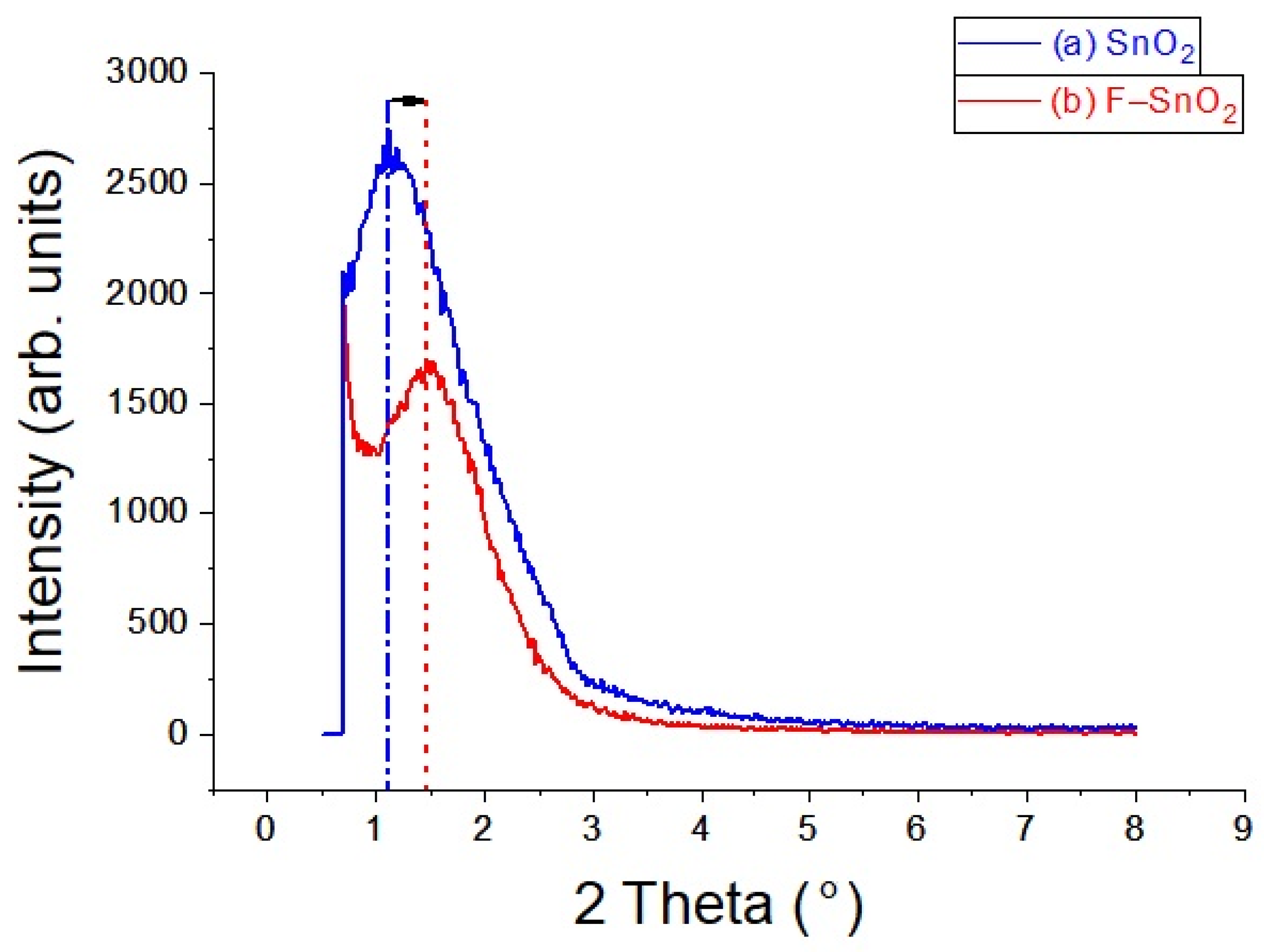
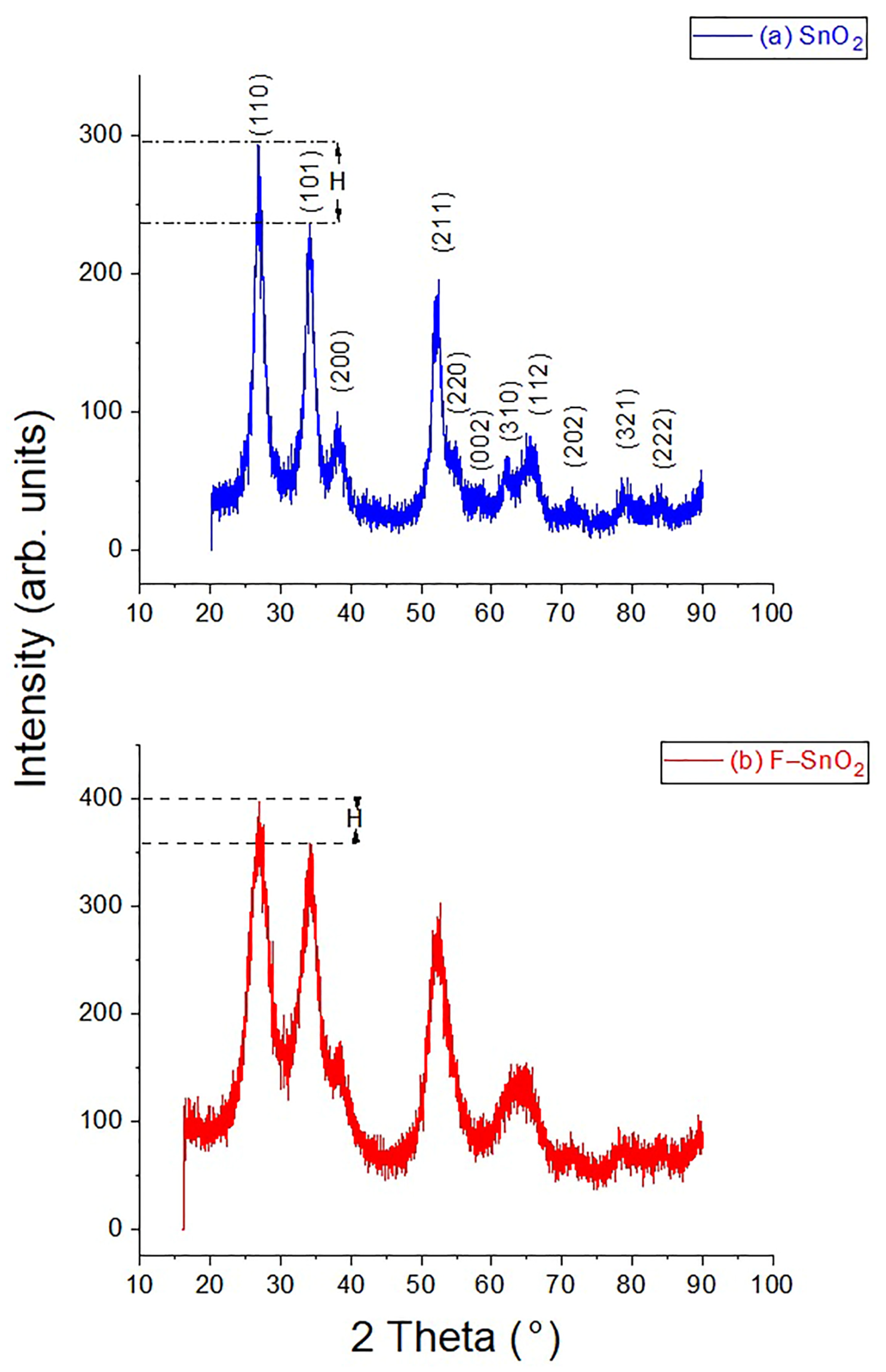
3.1. XRD

Low angle XRD patterns presented in Figure 1 reveal that both samples, SnO2 and F–SnO2, have mesoporous structures, from the presence of the main diffraction peak at (100). This peak shifted towards a larger angle when SnO2 was doped with fluorine, which indicates a slight decrease in the unit cell (a0) as a result of replacing some of the O atoms with F. The reduction in d-spacing (presented in Bragg’s law Equation (1)) is indicated by the dotted lines and the arrow in Figure 1.
d100 = n λ/2 sinθ
d100 = a0 sin60
where n is an integer, λ is the incident X-ray wavelength, and θ is the diffraction angle. The a0 in a porous structure represents a diffraction plane of straight distance between two adjacent pore centers that are separated by a wall thickness of material. The calculated a0 for SnO2 was 85.2 Å, whereas it was 68.5 Å for F–SnO2 Å. This decrease in a0 was the result of two factors: having a narrower pore size and incorporating fluorine atoms in the framework, which was more electronegative than oxygen [28,29]. This will shrink the crystallite sizes and the thickness of the wall between the pores. Notice that both samples underwent similar synthesis procedures and heat treatments. Moreover, the shapes of the main (100) diffraction peak for both materials SnO2 and F–SnO2 were similar, indicating that F atoms were well incorporated in the framework and did not upset the overall pore ordering in the structure. No other peaks were observed in this scan, indicating that there was no long-range ordering of the pores. This also indicates that most of the pores did not form tube-like shapes.
The wide-angle XRD patterns presented in Figure 2 show that both samples have a crystalline nature and that pure SnO2 was synthesized [30]. The diffraction peaks for both samples were indexed to the Cassiterite (tetragonal) structure of SnO2 [31,32]. No additional diffraction peaks appeared, indicating that the F species did not cluster or form a secondary phase outside the framework. This also confirms that the substitution of F ions did not affect the crystallinity of the material, [19,30] and that F ions were inserted into the framework [10]. Moreover, F favors the (101) plane [10,24], which is why the intensity of this plane was relatively higher in relation to the (110) plane for F–SnO2 in comparison with these planes of SnO2. That is why the height difference (H) was relatively smaller in F–SnO2 than in SnO2, as presented in Figure 2a,b. This also confirms that F is readily integrated in the framework of SnO2. Moreover, the (110) diffraction peak was used to calculate the average crystallite sizes for both samples by employing the Scherrer equation. The calculated average crystallite sizes were 4.1 and 3.4 nm for SnO2 and F–SnO2, respectively. The difference in the crystallite sizes agrees with and confirms the variation in the value of the unit cell a0 calculated in the low-angle XRD scan. These crystallite sizes confirm that SnO2 and F–SnO2 are both nanomaterials.

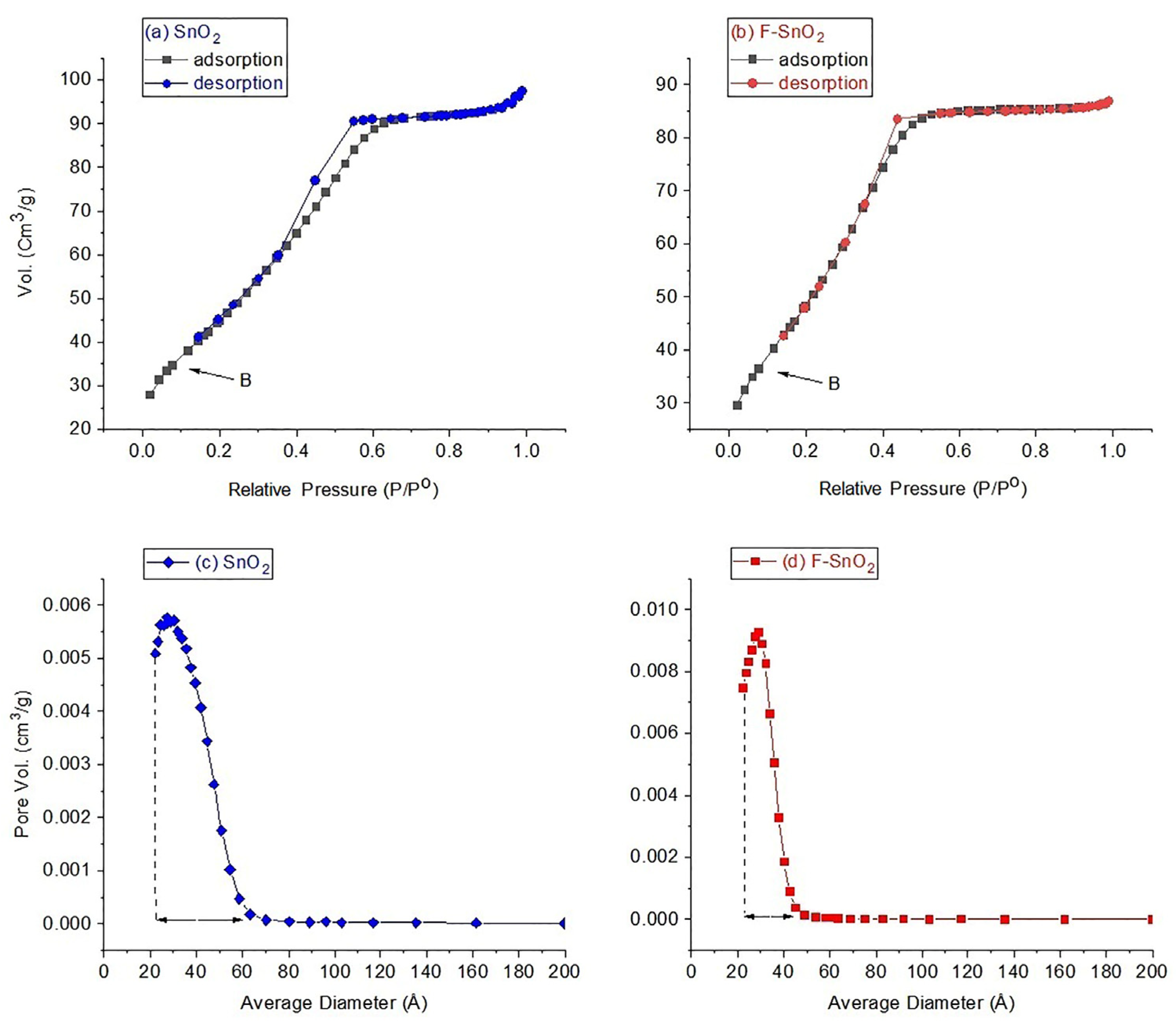
3.2. N2 Sorption Analysis
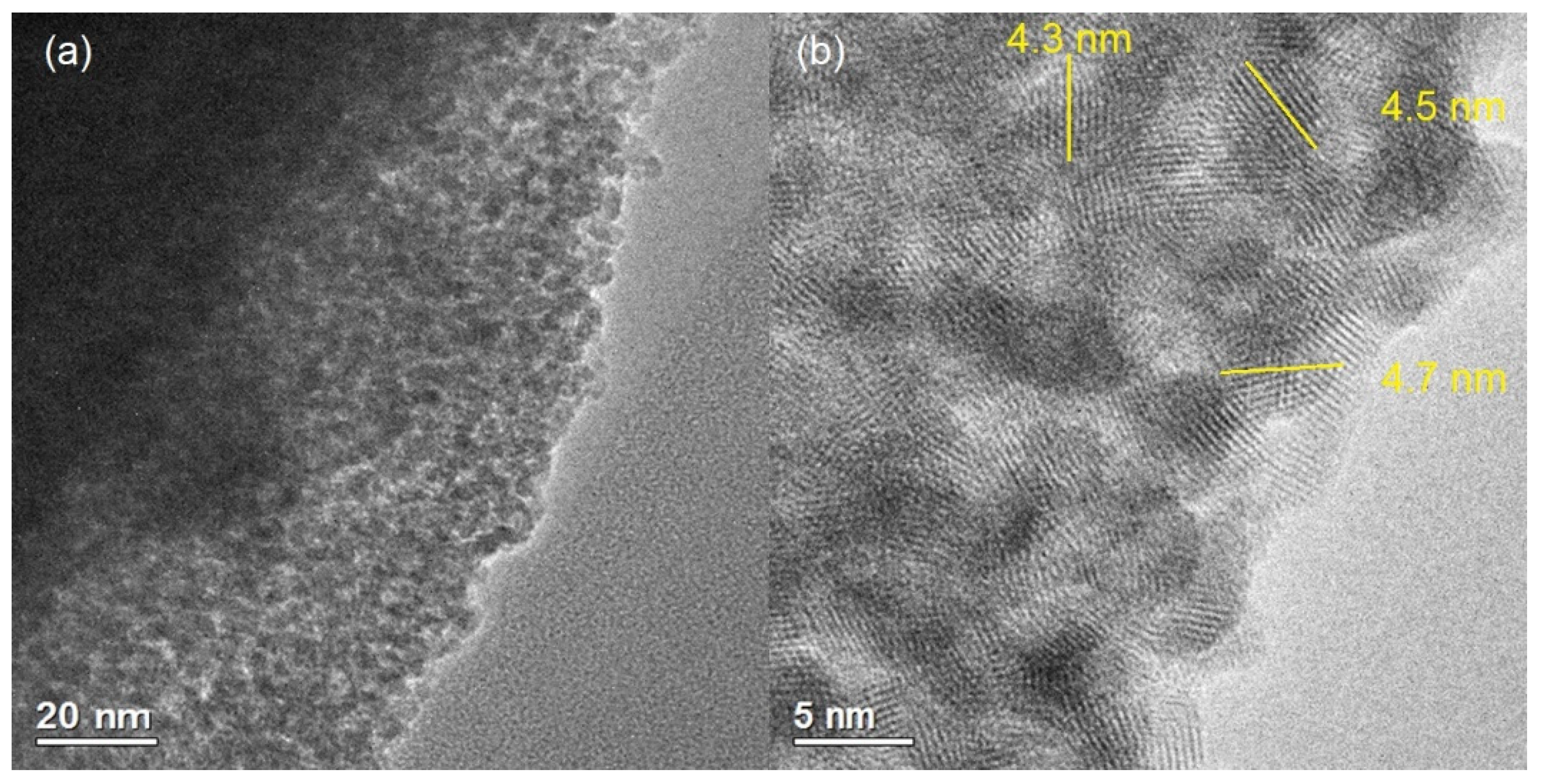
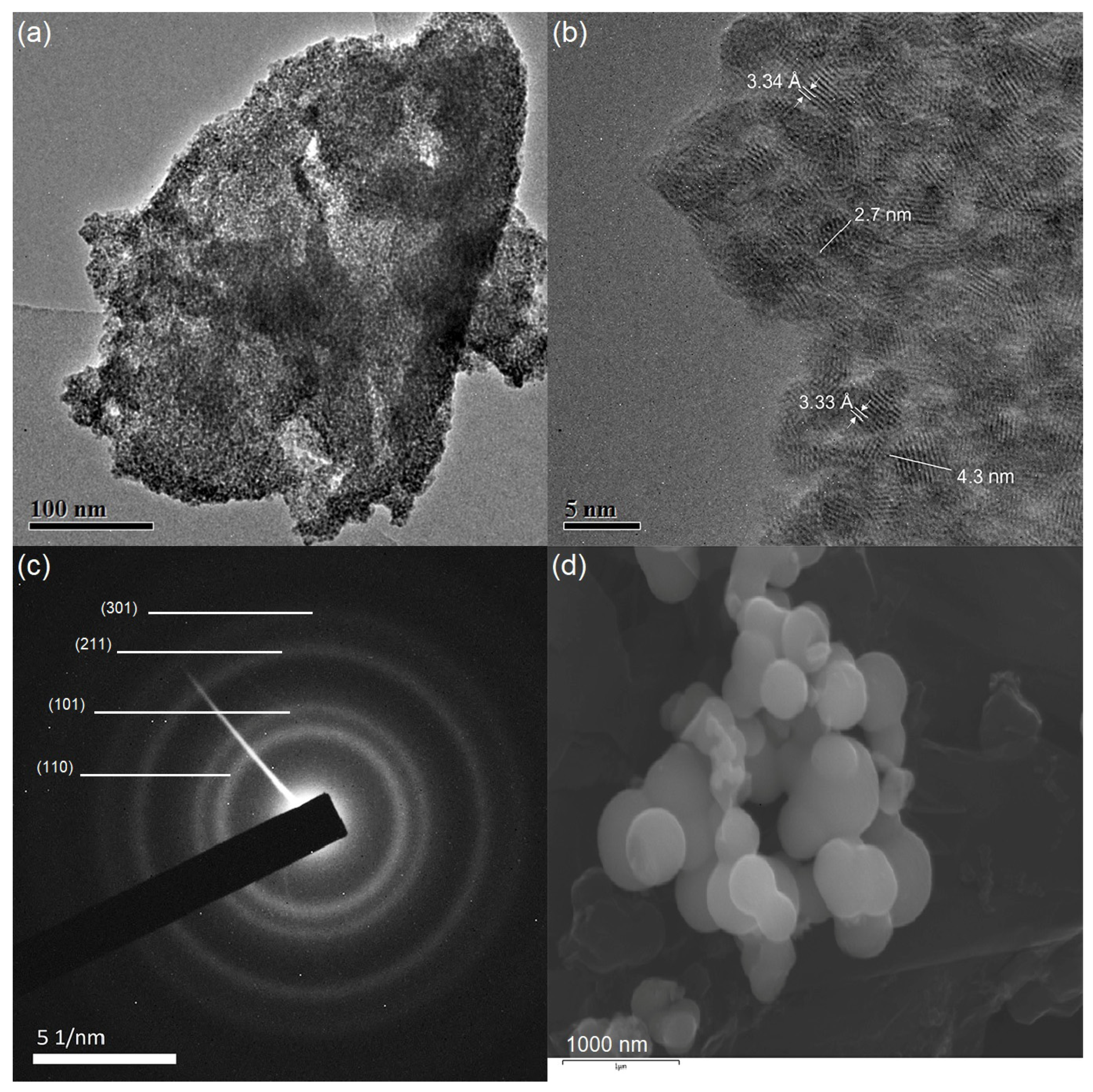
N2 adsorption/desorption analysis was performed on both materials, SnO2 and F–SnO2, with the resultant isotherm curves presented in Figure 3a,b. Both samples produced a type IVa isotherm [33], which was assigned to mesoporous materials. There were distinctive features of these isotherms, that the start of inflection point B (at 0.1 relative pressure) in these materials was not sharp, which is indicative that the mono layer was not completely covered by N2. Then, the coverage of N2 was extended for the mono and multi-layer at 0.2–0.6 relative pressure. After that, N2 capillary condensation occurred inside the pores before reaching the saturation pressure (p0), which was represented by the plateau between 0.6 and 0.9 relative pressure. Finally, a hysteresis curve (typical of IVa isotherms) occurred in the desorption cycle, which indicated the existence of some pores that exceeded the critical size of 4 nm in both materials. This hysteresis occurred when there was a slower rate of desorption than adsorption of N2. It is worth mentioning that the hysteresis curve was larger in the SnO2 sample than in F–SnO2, indicative that there were more large pores (larger than 4 nm) in SnO2 than in F–SnO2. This was also confirmed by the pore size distribution (Figure 3c,d), showing that sample SnO2 had a wider pore size distribution, falling in the range 2–6 nm. In contrast, the pore distribution in F–SnO2 was narrower, falling between 2 and 4 nm, as presented in Figure 3d.
Moreover, the BET surface areas obtained from SnO2 and F–SnO2 samples were 164 and 180 m2g−1, and the average pore size was 36.2 and 29.8 Å, respectively, presented in Figure 3c,d. Both N2 sorption results, the isotherm type and the pore size diameter, confirmed that SnO2 and F–SnO2 samples were classified as mesoporous materials according to IUPAC [33].

3.3. TEM

TEM images were acquired of SnO2 and F–SnO2 to give an insight into the crystallinity, pore location, and distribution in these materials. Figure 4a reveals that the pores were well distributed in SnO2 but were not uniform in size or shape, and SnO2 material surrounded these pores. Figure 4b confirmed that SnO2 is a crystalline material, which consists of semi-spherical crystallites that are fused together around the pores. Moreover, these crystallites vary in size and it is hard to determine the exact sizes of these crystallites using TEM images. Despite that, we managed to measure a few crystallite sizes that averaged to 4.5 nm, as indicated by yellow lines in Figure 4b. This size is similar to that calculated from wide-angle XRD.
Figure 5 represents TEM/HRTEM images acquired from F–SnO2. Figure 5a confirmed that the material contained pores, which spread across entire particles. Figure 5b is an HRTEM image of the particle in (a), showing crystalline fringes of 3.34 Å that can be assigned to the (110) plane of SnO2. In addition, the sample contained semi-spherical shaped crystallites that were fused together in a framework around the pores. The sizes of these crystals fell between 2.7 and 4.3 nm, as presented in Figure 5b, which agreed with the wide angle XRD calculation. Moreover, HRTEM images did not reveal any aggregates of F species or appear substantially different from SnO2, which further confirms that F was substituted into the framework. Figure 5c shows the electron diffraction pattern acquired from the particle in Figure 5a, indicating the polycrystalline structure of F–SnO2 with the diffraction rings indexed to tetragonal SnO2 [34]. The SEM image in Figure 5d confirmed that the semi-spherical shape of the F–SnO2 crystals were uniform and this shape was maintained to the micro level. This also confirmed that these micro grains were chemically fused together. This stacked growth promotes charge transfer.

3.4. EDX

The EDX spectrum shows the K and L peaks of all the elements present in the F–SnO2 sample, in Figure 6, which reveals that the sample composition contained Sn, O, and F atoms. This confirms that F was successfully incorporated in the F–SnO2 sample and it was part of its composition. The circled peak in Figure 6 clearly shows the Kα peak of F at 0.67 keV, which was adjacent to the Kα O peak and had almost been masked by it. The bonds and the chemical composition of these elements would be determined using XPS.

3.5. XPS

XPS analyses (Figure 7) were performed for both materials to investigate the surface and partial subsurface compositions and their oxidation states. XPS results in Figure 7a,b for both materials, SnO2 and F–SnO2, showed spin-orbit doublet peaks at 486.6 (Sn 3d5/2), 495.0 (Sn 3d3/2), and 487.1, 495.5 eV, respectively, plus 3d orbital splitting of 8.4 eV. This corresponded to the Sn4+ oxidation state of SnO2 [32,35]. The slight increment of 0.5 eV in the peaks of Sn 3d of the F–SnO2 sample could be attributed to the effect of the presence of the more electronegative F ions in the sample [10,36]. The XPS peak of O 1s spectra at 530.6, and 530.0 eV for SnO2 and F–SnO2, respectively, represented the lattice O2− species of SnO2 for both samples, Figure 7c,d [35,37]. The second O 1s XPS peak for both samples, at 531.6 and 531.7 eV, respectively, represented adsorbed surface oxygens that existed in the atmosphere, such as OH, H2O [37], and CO2 [34]. This did not exclude the presence of oxygen vacancies which had the same XPS binding energies around these values, 531.7 eV [38]. This was also confirmed by the atomic ratio collected from the XPS data, O/Sn of 2.1 and 2.3 at. % for SnO2 and F–SnO2, respectively, showing extra oxygen species adsorbed at the surface for both samples, but was more pronounced for the F–SnO2 sample. This is because F is more electronegative than Sn, making Sn4+ more positively charged [32]. This will make Sn attract a more negatively charged oxygen species. Furthermore, the XPS peak at 684.6 eV in Figure 7e, whose binding energy corresponded to F 1s, which replaced some oxygen (O2−) in the lattice of F–SnO2, confirms that F became a single electron donor [10,24]. In addition, the F wt./wt. percentage calculated from XPS data was 1.1% F/SnO2 (1.4% F/Sn), which was less than the intended percentage calculated theoretically during the synthesis procedure, which was 3%. This decrease may occur during the washing of the as-synthesized sample or during the Soxhlet extraction steps, both of which were performed before the calcination step. During calcination, more condensation occurred in the framework that strengthened the bonds between the atoms in the structure. Therefore, we think that the lost F species were superficial and they did not form bonds deep in the structural framework.

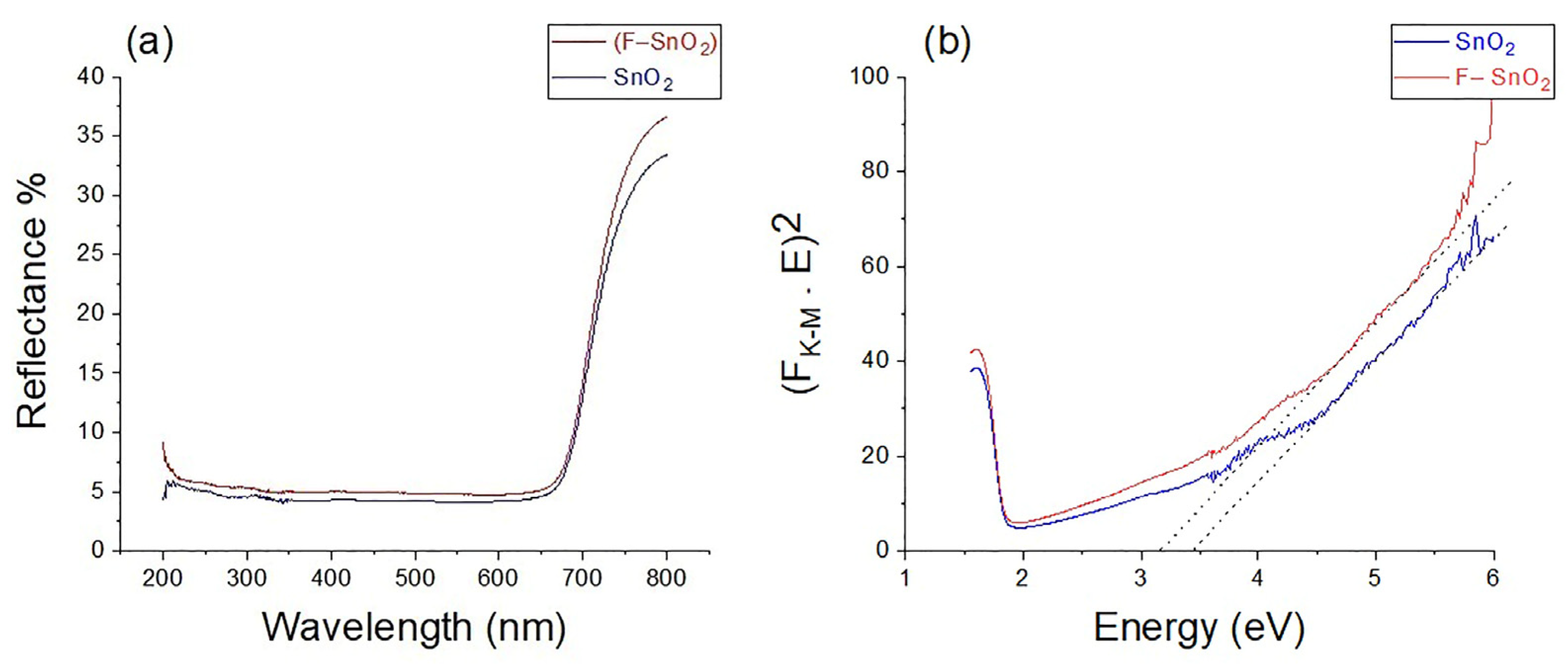
3.6. UV-Visible Spectroscopy

The diffuse reflectance (R) Figure 8a was performed for both samples to be converted into the Kubelka–Munk function (FK–M) to produce the Tauck plot. The reflection of both materials was less than 7% in the UV until the red-light range, at which both reflections increased above 30% (Figure 8a). This indicates that both materials had high transmission values in these regions [28]. The constructed Tauck plot in Figure 8b was employed to determine the band gap of these materials, basically plotting (FK–M × E)2 against the energy (E) at which the intercept of the tangent gives the direct optical band gap of the material [39,40,41].
The following equation explains the FK–M:
FK–M (R) = (1 − R)2/2R
E =
(αhν)2 = A (hv − Eg)
where α is the absorption coefficient, h is Plank’s constant, v is light frequency, A is constant, and Eg is the direct band gap energy [38]. FK–M = α/s, where s is the scattering coefficient. The band gaps for SnO2 and F–SnO2 were 3.40 and 3.16 eV, respectively, as shown by the tangent dotted lines in the Tauck plot shown in Figure 8b. The lower band gap of both materials could be the result of many factors. First, having long chemically connected structures (chain-like) reduces the band gap [42]. The second factor is because of strains caused by having SnO2 thin walls, which narrow the gap distance between conduction and valence bands [43]. Third is the probability of having an intermediate SnOx band [44], and the existence of an intermediate defect band of oxygen vacancies that appears above the valence band of SnO2 [12,13,45]. This also confirms that doping SnO2 with F decreases the bandgap, most likely by creating a defect band below the conductance band [44,46,47]. On the other hand, these bandgap values suggest that SnO2 and F–SnO2 would be optically excited by UV-A light at and below 365 and 392 nm, respectively. Furthermore, this 392 nm wavelength calculated for F–SnO2 was very close to the visible violet border wavelength of 400 nm, which was the border of visible light.

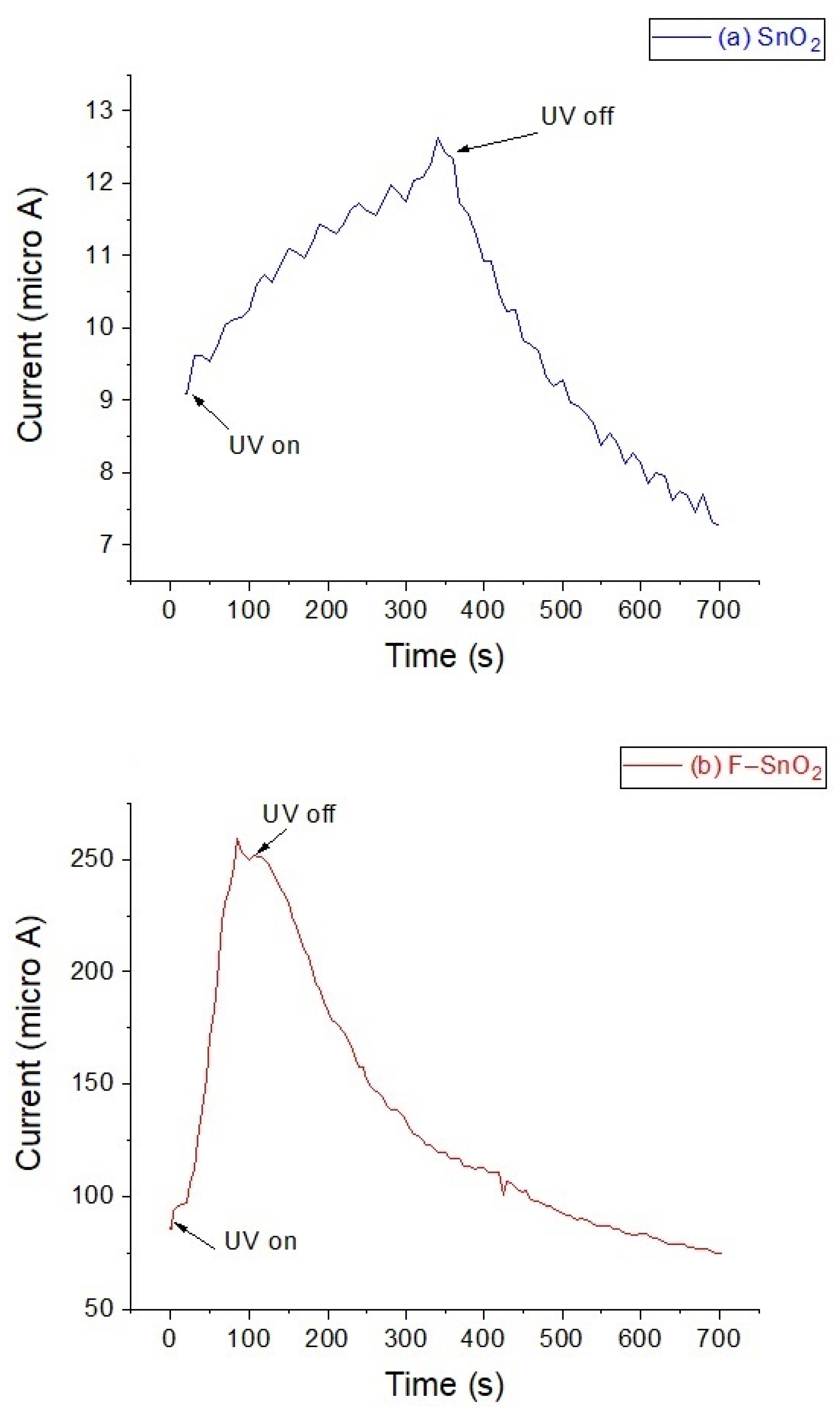
3.7. Conductivity and Opti-Electronic Tests

The conductivity of both materials, SnO2 and F–SnO2, was measured in air at 25 °C with the conductance being 5 × 10⁻⁵ and 4.8 × 10⁻³ S/m, respectively. This confirms that adding 1% of F to SnO2 increased the conductivity by 100 times. By donating more free charges to the framework, and strengthening the framework connectivity (as discussed in Section 3.3), this facilitated charge transfer.
To study the optoelectronic excitation effect of the materials, both samples were subjected to UV light for a few minutes, while the current produced was recorded simultaneously, as presented in Figure 9. This current was a measure of the excited electrons (e) coming from the valence band hopping to the conduction band for the semiconductor materials [38]. Initially, SnO2 was exposed to UV light for 5 min, at which point the current increased to a maximum of 12.6 μA. After that, the UV source was switched off and the recorded current continued to decline, as shown in Figure 9a. F–SnO2 was then subjected to the same source for 2 min, and when the UV light was on the current increased sharply from 70 to 259 μA. Next, this source switched off and the current started to decline gradually to the end of the test (Figure 9b). This produced a current that was about 20 times larger than that of SnO2. This test confirmed two points, firstly that both samples can be optically excited under wavelengths at/or below 365 for SnO2 and 392 nm for F–SnO2. Secondly, F–SnO2 is more optically active than SnO2 at similar experimental conditions; this could be the result of having a smaller band gap. This smaller band gap allowed more charges to be excited at this wavelength (365 nm) than in pristine SnO2. This could be the result of having an electron donor fluoride ion in the framework, more charges available, and faster charge transfer because of a more compacted structure.

4. Conclusions

We successfully synthesized a crystalline mesoporous tin dioxide nanomaterial doped with fluoride in one pot at an ambient pressure and temperature (using our modified method). The crystallites of this material were chemically connected in a continuous framework. F–SnO2 possessed high electrical conductivity in air 4.8 × 10⁻³ S/m, which was 100 times larger than pristine SnO2. F–SnO2 was approximately 20 times more optically active than pristine SnO2 under a UV source. As a result of having F in the framework, this made the structure more compact and connected. In addition, F is an electron donor ion. Moreover, F–SnO2 has a high BET surface area of 180 m2g−1, an average crystallite size of 3.4 nm, and a narrow pore size distribution of 2–4 nm, which promotes this material to be readily employed in optoelectronic cells and instruments.

Author Contributions

T.A. synthesized the materials and performed structural and compositional analyses using XPS, XRD, N2 sorption analysis, UV-visible spectroscopy, conductivity, and opto-electronic tests and discussed these techniques and part of the SEM/TEM/EDX results in the manuscript. T.A. wrote most of the manuscript and provided financial support from PAAET. H.F.G. performed the TEM, HRTEM, SEM, and EDX characterization, discussed the obtained results, and revised the manuscript several times during the writing process. All authors have read and agreed to the published version of the manuscript.

Funding

This project was funded by the Public Authority of Applied Education and Training (PAAET), Kuwait (Project No. BE-16-05).

Data Availability Statement

Not applicable.

Acknowledgments

Assistance provided at Kuwait University for the XPS measurements (Project No. GS01/05) is acknowledged.

Conflicts of Interest

The authors declare no conflict of interest.

References

  1. Aswaghosh, L.; Manoharan, D.; Jaya, N.V. Defect structure and optical phonon confinement in ultrananocrystalline BixSn1-xO2 (x = 0, 0.03, 0.05, and 0.08) synthesized by a sonochemical method. Phys. Chem. Chem. Phys. 2016, 18, 5995–6004. [Google Scholar] [CrossRef] [PubMed]
  2. Shaalan, N.M.; Hamad, D.; Abdel-Latief, A.Y.; Abdel-Rahim, M.A. Preparation of quantum size of tin oxide: Structural and physical characterization. Prog. Nat. Sci. Mater. Int. 2016, 26, 145–151. [Google Scholar] [CrossRef]
  3. Wagner, T.; Bauer, M.; Sauerwald, T.; Kohl, C.D.; Tiemann, M. X-ray absorption near-edge spectroscopy investigation of the oxidation state of Pd species in nanoporous SnO2 gas sensors for methane detection. Thin Solid Films 2011, 520, 909–912. [Google Scholar] [CrossRef]
  4. Li, X.; Cho, J.H.; Kurup, P.; Gu, Z. Novel sensor array based on doped tin oxide nanowires for organic vapor detection. Sens. Actuators B Chem. 2012, 162, 251–258. [Google Scholar] [CrossRef]
  5. Brunet, E.; Maier, T.; Mutinati, G.C.; Steinhauer, S.; Köck, A.; Gspan, C.; Grogger, W. Comparison of the gas sensing performance of SnO2 thin film and SnO2 nanowire sensors. Sens. Actuators B Chem. 2012, 165, 110–118. [Google Scholar] [CrossRef]
  6. Yu, W.; Jiang, K.; Wu, J.; Gan, J.; Zhu, M.; Hu, Z.; Chu, J. Electronic structures and excitonic transitions in nanocrystalline iron-doped tin dioxide diluted magnetic semiconductor films: An optical spectroscopic study. Phys. Chem. Chem. Phys. 2011, 13, 6211–6222. [Google Scholar] [CrossRef]
  7. Ganose, A.M.; Scanlon, D.O. Band gap and work function tailoring of SnO2 for improved transparent conducting ability in photovoltaics. J. Mater. Chem. C 2016, 4, 1467–1475. [Google Scholar] [CrossRef]
  8. Huang, B.J.; Li, F.; Zhang, C.W.; Li, P.; Wang, P.J. Electronic structure and optical properties of Ag-doped SnO2 nanoribbons. RSC Adv. 2014, 4, 41819–41824. [Google Scholar] [CrossRef]
  9. Dalapati, G.K.; Sharma, H.; Guchhait, A.; Chakrabarty, N.; Bamola, P.; Liu, Q.; Saianand, G.; Sai Krishna, A.M.; Mukhopadhyay, S.; Dey, A.; et al. Tin oxide for optoelectronic, photovoltaic and energy storage devices: A review. J. Mater. Chem. A 2021, 9, 16621–16684. [Google Scholar] [CrossRef]
  10. Noor, N.; Parkin, I.P. Enhanced transparent-conducting fluorine-doped tin oxide films formed by Aerosol-Assisted Chemical Vapour Deposition. J. Mater. Chem. C 2013, 1, 984–996. [Google Scholar] [CrossRef]
  11. Morris, L.; Williams, D.E.; Kaltsoyannis, N.; Tocher, D.A. Surface grafting as a route to modifying the gas-sensitive resistor properties of semiconducting oxides: Studies of Ru-grafted SnO2. Phys. Chem. Chem. Phys. 2001, 3, 132–145. [Google Scholar] [CrossRef]
  12. Liu, L.; Shu, S.; Zhang, G.; Liu, S. Highly Selective Sensing of C2H6O, HCHO, and C3H6O Gases by Controlling SnO2 Nanoparticle Vacancies. ACS Appl. Nano Mater. 2018, 1, 31–37. [Google Scholar] [CrossRef]
  13. Manikandan, M.; Tanabe, T.; Ramesh, G.V.; Kodiyath, R.; Ueda, S.; Sakuma, Y.; Homma, Y.; Dakshanamoorthy, A.; Ariga, K.; Abe, H. Tailoring the surface-oxygen defects of a tin dioxide support towards an enhanced electrocatalytic performance of platinum nanoparticles. Phys. Chem. Chem. Phys. 2016, 18, 5932–5937. [Google Scholar] [CrossRef] [PubMed]
  14. Brus, L.E. Electron-electron and electron-hole interactions in small semiconductor crystallites: The size dependence of the lowest excited electronic state. J. Chem. Phys. 1984, 80, 4403–4409. [Google Scholar] [CrossRef]
  15. Martinez, C.J.; Hockey, B.; Montgomery, C.B.; Semancik, S. Porous tin oxide nanostructured microspheres for sensor applications. Langmuir 2005, 21, 7937–7944. [Google Scholar] [CrossRef]
  16. Smith, A.M.; Nie, S. Bright and compact alloyed quantum dots with broadly tunable near-infrared absorption and fluorescence spectra through mercury cation exchange. J. Am. Chem. Soc. 2011, 133, 24–26. [Google Scholar] [CrossRef]
  17. Aqeel, T.; Greer, H.F.; Zhou, W.Z.; Bruce, D.W.; Bumajdad, A. Novel Direct Synthesis of Mesoporous Tin Dioxide Network Intact up to 500 °C. J. Nano Res. 2016, 40, 79–89. [Google Scholar] [CrossRef]
  18. Goebbert, C.; Aegerter, M.A.; Burgard, D.; Nassb, R. Ultrafiltration conducting membranes and coatings from. J. Mater. Chem. 1999, 9, 253–258. [Google Scholar] [CrossRef]
  19. Oakton, E.; Tillier, J.; Siddiqi, G.; Mickovic, Z.; Sereda, O.; Fedorov, A.; Copéret, C. Structural differences between Sb- and Nb-doped tin oxides and consequences for electrical conductivity. New J. Chem. 2016, 40, 2655–2660. [Google Scholar] [CrossRef]
  20. Yamazoe, N.; Sakai, G.; Shimanoe, K. Oxide semiconductor gas sensors. Catal. Surv. Asia 2003, 7, 63–75. [Google Scholar] [CrossRef]
  21. Sevier, E.I.; Aegerter, M.A.; Reich, A.; Ganz, D.; Gasparro, G.; Piitz, J.; Krajewski, T. Comparative study of SnO2: Sb transparent conducting films produced by various coating and heat treatment techniques. J. Non Cryst. Solids 1997, 218, 123–128. [Google Scholar]
  22. Zhong, X.; Yang, B.; Zhang, X.; Jia, J.; Yi, G. Effect of calcining temperature and time on the characteristics of Sb-doped SnO2 nanoparticles synthesized by the sol-gel method. Particuology 2012, 10, 365–370. [Google Scholar] [CrossRef]
  23. Terrier, C.; Chatelon, J.P.; Roger, J.A. Electrical and optical properties of Sb:SnO2 thin films obtained by the sol-gel method. Thin Solid Films 1997, 295, 95–100. [Google Scholar] [CrossRef]
  24. Noor, N.; Chew, C.K.T.; Bhachu, D.S.; Waugh, M.R.; Carmalt, C.J.; Parkin, I.P. Influencing FTO thin film growth with thin seeding layers: A route to microstructural modification. J. Mater. Chem. C 2015, 3, 9359–9368. [Google Scholar] [CrossRef]
  25. Burawoy, A. Distance, Bond energy, bond distance, and the nature of the covalent linkage. Trans. Faraday Soc. 1943, 39, 79–90. [Google Scholar] [CrossRef]
  26. Kojima, M.; Kato, H.; Gatto, M. Microstructure and electrical properties of Sb-Sn-O thin films. J. Non Cryst. Solids 1997, 218, 230–234. [Google Scholar] [CrossRef]
  27. Severin, K.G.; Abdel-Fattah, T.M.; Pinnavala, T.J. Supramolecular assembly of mesostructured tin oxide. Chem. Commun. 1998, 14, 1471–1472. [Google Scholar] [CrossRef]
  28. Ponja, S.D.; Williamson, B.A.D.; Sathasivam, S.; Scanlon, D.O.; Parkin, I.P.; Carmalt, C.J. Enhanced electrical properties of antimony doped tin oxide thin films deposited: Via aerosol assisted chemical vapour deposition. J. Mater. Chem. C 2018, 6, 7257–7266. [Google Scholar] [CrossRef]
  29. Du, Y.; Yan, J.; Meng, Q.; Wang, J.; Dai, H. Fabrication and excellent conductive performance of antimony-doped tin oxide-coated diatomite with porous structure. Mater. Chem. Phys. 2012, 133, 907–912. [Google Scholar] [CrossRef]
  30. Wang, Y.; Brezesinski, T.; Antonietti, M.; Smarsly, B. Ordered Mesoporous Sb-Nb-Ta. Am. Chem. Soc. Nano 2009, 3, 1373–1378. [Google Scholar]
  31. Oh, H.S.; Nong, H.N.; Strasser, P. Preparation of mesoporous Sb-, F-, and in-doped SnO2 bulk powder with high surface area for use as catalyst supports in electrolytic cells. Adv. Funct. Mater. 2015, 25, 1074–1081. [Google Scholar] [CrossRef]
  32. Hao, T.; Cheng, G.; Ke, H.; Zhu, Y.; Fu, Y. Effects of fluorine ions on the formation and photocatalytic activities of SnO2 nanoparticles with small sizes. RSC Adv. 2014, 4, 21548–21552. [Google Scholar] [CrossRef]
  33. Thommes, M.; Kaneko, K.; Neimark, A.V.; Olivier, J.P.; Rodriguez-Reinoso, F.; Rouquerol, J.; Sing, K.S.W. Physisorption of gases, with special reference to the evaluation of surface area and pore size distribution (IUPAC Technical Report). Pure Appl. Chem. 2015, 87, 1051–1069. [Google Scholar] [CrossRef]
  34. Nag, P.; Majumdar, S.; Bumajdad, A.; Devi, P.S. Enhanced gas sensing performance of tin dioxide-based nanoparticles for a wide range of concentrations of hydrogen gas. RSC Adv. 2014, 4, 18512–18521. [Google Scholar] [CrossRef]
  35. Lee, S.; Galstyan, V.; Ponzoni, A.; Gonzalo-juan, I.; Riedel, R.; Dourges, M.; Nicolas, Y.; Toupance, T. Finely Tuned SnO2 Nanoparticles for Efficient Detection of Reducing and Oxidizing Gases: The Influence of Alkali Metal Cation on Gas- Sensing Properties. ACS Appl. Mater. Interfaces 2018, 10, 10173–10184. [Google Scholar] [CrossRef] [PubMed]
  36. Sun, J.; Yin, G.; Cai, T.; Yu, W.; Peng, F.; Sun, Y.; Zhang, F.; Lu, J.; Ge, M.; He, D. The role of oxygen vacancies in the sensing properties of Ni substituted SnO2 microspheres. RSC Adv. 2018, 8, 33080–33086. [Google Scholar] [CrossRef] [PubMed]
  37. Uddin, M.T.; Nicolas, Y.; Olivier, C.; Toupance, T.; Servant, L.; Müller, M.M.; Kleebe, H.J.; Ziegler, J.; Jaegermann, W. Nanostructured SnO2-ZnO heterojunction photocatalysts showing enhanced photocatalytic activity for the degradation of organic dyes. Inorg. Chem. 2012, 51, 7764–7773. [Google Scholar] [CrossRef] [PubMed]
  38. Liang, Y.C.; Lo, Y.J. High-temperature solid-state reaction induced structure modifications and associated photoactivity and gas-sensing performance of binary oxide one-dimensional composite system. RSC Adv. 2017, 7, 29428–29439. [Google Scholar] [CrossRef]
  39. Goodall, J.B.M.; Kellici, S.; Illsley, D.; Lines, R.; Knowles, J.C.; Darr, J.A. Optical and photocatalytic behaviours of nanoparticles in the Ti-Zn-O binary system. RSC Adv. 2014, 4, 31799–31809. [Google Scholar] [CrossRef]
  40. Rashad, M.M.; Ismail, A.A.; Osama, I.; Ibrahim, I.A.; Kandil, A.H.T. Photocatalytic decomposition of dyes using ZnO doped SnO2 nanoparticles prepared by solvothermal method. Arab. J. Chem. 2014, 7, 71–77. [Google Scholar] [CrossRef]
  41. Elsayed, A.M.; Rabia, M.; Shaban, M.; Aly, A.H.; Ahmed, A.M. Preparation of hexagonal nanoporous Al2O3/TiO2/TiN as a novel photodetector with high efficiency. Sci. Rep. 2021, 11, 17572. [Google Scholar] [CrossRef] [PubMed]
  42. Nithiyanantham, U.; Ramadoss, A.; Kundu, S. Synthesis and characterization of DNA fenced, self-assembled SnO2 nano-assemblies for supercapacitor applications. Dalton Trans. 2016, 45, 3506–3521. [Google Scholar] [CrossRef] [PubMed]
  43. Zhou, W.; Liu, Y.; Yang, Y.; Wu, P. Band gap engineering of SnO2 by epitaxial strain: Experimental and theoretical investigations. J. Phys. Chem. C 2014, 118, 6448–6453. [Google Scholar] [CrossRef]
  44. Popescu, D.A.; Herrmann, J.; Chimie, D.; Paris, U.; Diderot, D.; April, A. Nanosized tin dioxide: Spectroscopic (UV—VIS, NIR, EPR) and electrical conductivity studies. Phys. Chem. Chem. Phys. 2001, 3, 2522–2530. [Google Scholar] [CrossRef]
  45. Batzill, M.; Diebold, U. Surface studies of gas sensing metal oxides. Phys. Chem. Chem. Phys. 2007, 9, 2307–2318. [Google Scholar] [CrossRef]
  46. Sergeienko, S.A.; Kukla, A.L.; Yaremov, P.S.; Kiriienko, P.I.; Shvets, A.V.; Nauky, P.; Nauky, P. Effect of synthesis and doping conditions on the physical and chemical properties of mesoporous tin dioxide. Theor. Exp. Chem. 2012, 48, 245–251. [Google Scholar] [CrossRef]
  47. Sergiienko, S.A.; Kukla, O.L.; Yaremov, P.S.; Solomakha, V.N.; Shvets, O.V. The influence of preparation conditions and doping on the physicochemical and sensor properties of mesoporous tin oxide. Sens. Actuators B Chem. 2013, 177, 643–653. [Google Scholar] [CrossRef]
Figure 1. Low-angle XRD patterns of (a) SnO2 and (b) F–SnO2.
Nanomaterials 13 02731 g001
Figure 2. Wide angle XRD patterns of (a) SnO2 and (b) F–SnO2.
Nanomaterials 13 02731 g002
Figure 3. N2 sorption isotherms of (a) SnO2, (b) F–SnO2, and the corresponding pore size distributions of (c) SnO2 and (d) F–SnO2.
Nanomaterials 13 02731 g003
Figure 4. (a) TEM and (b) HRTEM images of SnO2.
Nanomaterials 13 02731 g004
Figure 5. (a,b) TEM/HRTEM images of F–SnO2, (c) selected area electron diffraction pattern acquired from the particle in (a,b), and (d) SEM image of F–SnO2.
Nanomaterials 13 02731 g005
Figure 6. EDX spectrum of F–SnO2 sample.
Nanomaterials 13 02731 g006
Figure 7. XPS spectra for SnO2 and F–SnO2 (a,b) Sn 3d, (c,d) O 1s, and (e) F 1s regions.
Nanomaterials 13 02731 g007
Figure 8. (a) Reflectance % and (b) the Tuck plot for SnO2 and F–SnO2, respectively.
Nanomaterials 13 02731 g008
Figure 9. Current produced per second by exposing the samples to UV radiation: (a) SnO2 and (b) F–SnO2.
Nanomaterials 13 02731 g009
Disclaimer/Publisher’s Note: The statements, opinions and data contained in all publications are solely those of the individual author(s) and contributor(s) and not of MDPI and/or the editor(s). MDPI and/or the editor(s) disclaim responsibility for any injury to people or property resulting from any ideas, methods, instructions or products referred to in the content.

