Abstract
Si1−xGex nanowires (NWs) were prepared by gold-supported chemical vapor deposition (CVD) using a single-source precursor with preformed Si–Ge bonds. Besides the tamed reactivity of the precursor, the approach reduces the process parameters associated with the control of decomposition characteristics and the dosing of individual precursors. The group IV alloy NWs are single crystalline with a constant diameter along their axis. During the wire growth by low pressure CVD, an Au-containing surface layer on the NWs forms by surface diffusion from the substrate, which can be removed by a combination of oxidation and etching. The electrical properties of the Si1−xGex/Au core-shell NWs are compared to the Si1−xGex NWs after Au removal. Core–shell NWs show signatures of metal-like behavior, while the purely semiconducting NWs reveal typical signatures of intrinsic Si1−xGex. The synthesized materials should be of high interest for applications in nano- and quantum-electronics.
1. Introduction
Semiconductor nanowires (NWs) play a major role in intriguing technological applications in the field of high-performance nanoelectronics [1], photovoltaics [2], photonics [3], thermoelectrics [4,5], chemical energy storage [6], and biomedicine [7]. Different aspects of semiconductor NW research have been reviewed and the fundamental growth, structure, and property relations have been described [8,9,10,11,12,13,14]. Among this wide field, group IV materials are of specific interest as these materials could be easily integrated into current device processing approaches.
Today, Si1−xGex is already a key material in modern high-speed bipolar transistors. Most notably, Si1−xGex and Ge have been identified as promising channel materials for field-effect transistors (FETs) to enable higher drive currents, a reduction in dynamic power consumption, and enhanced switching speeds compared with conventional Si devices [15]. The group IV substitutional solid solution Si1−xGex is an alloy with complete solubility over the whole composition range [16]. Si1−xGex nanostructures are extensively used in a large portfolio of applications including advanced transistors, quantum devices, photodetectors, electro-optical modulators, photovoltaics, microelectromechanical systems (MEMS), and thermoelectric generators [17,18,19,20,21,22,23]. Moreover, Si1−xGex interlayers can be used to control strain and defect densities in Si and Ge layers for electrical applications in CMOS device architectures [24,25,26]. In addition, the first significant observations of band edge photoluminescence were also based on fully strained Si1−xGex [27,28]. The electrical properties of the Si1−xGex substitutional solid solution with cubic crystal phase have been summarized [29], but new developments can benefit from molecular precursors providing pre-formed Si-Ge building blocks.
The controlled synthesis of thin layers and nanostructures of Si1−xGex is typically based on molecular beam epitaxy using the elements as sources [30,31,32] and mixtures of SiH4/GeH4 as precursors in chemical vapor deposition [33,34]. Similarly, Si1−xGex NW growth has been described by metal-supported CVD using individual Ge and Si precursors by various groups [35,36,37].
The single-source precursor approach was successfully demonstrated for different binary materials in the past [38,39,40,41]. More specifically, previously described single-source precursors for Si1−xGex material carrying exclusively hydride ligands are pyrophoric and require rigorous safety measures similar to the individual SiH4 and GeH4 sources [42,43], which makes the approach described here using a less reactive precursor intriguing. For the thermal conversion of precursors to Si1−xGex, it should be noted that Si–C-containing silanes typically lead to silicon carbide [44,45,46,47], while Ge–C can be cleaved even at very moderate temperatures, yielding pure Ge material [48,49,50]. Applications based on non-pyrophoric single-source precursors for Si1−xGex synthesis combine easier handling with a simplified parameter set to control the materials’ synthesis, representing a viable alternative to the conventional approaches.
Here, we report on the Au-assisted CVD synthesis of NWs using (H3Si)2Ge(nBu)2 precursor and their structural as well as chemical characterization by μ-Raman spectroscopy, energy dispersive X-ray spectroscopy (EDX), scanning electron microscopy (SEM), and transmission electron microscopy (TEM). The electrical properties were investigated in two- and four-probe geometry and reveal differences in the behavior between Si1−xGex/Au core–shell NWs and Si1−xGex NWs.
2. Materials and Methods
CVD Process and Thin Film Characterization
CVD was carried out in a home-built cold-wall reactor using high-frequency heating of a graphite or steel susceptor for indirect heating of sapphire (0001) (Crystal GmbH, Berlin, Germany). Prior to use, the substrates are coated with a ~5 nm Au film by sputtering. The substrates are attached to the susceptor by silver paste to ensure efficient thermal contact. Substrate temperatures were limited to TS = 750–783 K. The precursor was introduced into the reactor through a glass flange applying a dynamic vacuum (~10−6 mbar) while keeping the precursor temperatures in the range of 253–258 K using a cooling bath based on chilled isopropyl alcohol as a coolant. Typically, 40–80 mg of the (H3Si)2Ge(nBu)2 precursor was used as source for the CVD experiments and the growth was carried out for 60–90 min. Growth experiments with similar parameters were verified at least three times. Typically, higher substrate temperatures also result in higher density of NWs, but differ in the microstructure as described below. The detailed description of the precursor synthesis has been published recently [51]. A similar CVD setup has been described in the literature for the growth of thin films and nanostructures using molecular sources [52,53].
The Au removal was carried out by post-growth oxidation at 1173 K for 20 min under 50 sccm oxygen flow. The oxide was removed by 60 s etching using buffered HF, which is an ammonium fluoride etching mixture solution (Sigma-Aldrich, St. Louis, MO, USA). Finally, the Au was removed by 60 s etching using commercial KI/I2 solution purchased from Sigma-Aldrich. The NWs were washed twice with deionized water and once with isopropyl alcohol. Electron beam lithography was used to define the electrodes and Al was sputtered as electrode material using similar steps as described in the literature [54] and an additional HF dip before Al deposition.
A JEOL JEM-3000F equipped with a Schottky field-emission electron source operating at 300 kV was used to acquire TEM images, HAADF-STEM images, STEM-EDX line scans, and STEM-EDS elemental maps. TEM images were recorded with a charge-coupled device (CCD) camera (GATAN Orius camera). An Oxford Instruments INCA system and an 80 mm2 silicon drift detector (SDD) were used to perform EDX analyses. The data were acquired and processed with DigitalMicrograph from Gatan (Version 2.31.734.0/DigitalMicrograph™ 3.9.3 for GMS 1.4.3) and INCA from Oxford Instruments Nanotechnology Tools Ltd. (Version 4.15).
The μ-Raman measurements were performed on a WITec Alpha300 Raman system with a frequency-doubled Nd:YAG laser (λ = 532 nm) in a backscattering geometry. The power of the incident laser was adjusted to 100 μW to prevent heated up of the NWs. The laser was focused through an achromatic Nikon EPI EPlan 100× objective (NA = 0.9, WD = 0.23 mm), enabling a diffraction limited spot size of ~720 nm. The integration time was set to 60 s.
The electrical measurements were conducted at room temperature and ambient conditions using a HP 4156B semiconductor analyzer and a probe station placed in a shielded dark box to exclude the influence of ambient light and electromagnetic fields.
3. Results
Low-pressure CVD (LPCVD) without a carrier gas was used to grow Si1−xGex NWs on Au-coated sapphire substrates. The recently described single-source precursor (H3Si)2Ge(nBu)2 containing Si and Ge in one molecule was used for the NW synthesis [51]. This molecular source reduces parameters for the precursor delivery when compared with individual precursors and, at the same time, its reduced reactivity allows for more convenient handling without elaborate safety measures. For NW growth, the liquid precursor (H3Si)2Ge(nBu)2 was kept at 250–255 K during the LPCVD owing to its high vapor pressure. Figure 1a illustrates the efficient formation of Si1−xGex NWs on Au-coated sapphire substrates. The NW density, very low tapering tendency, and their length are ideal for following electrical characterization. The expected Au seed is always observed at the tip of each NW, which is a signature of the NW growth according to the vapor–liquid–solid (VLS) mechanism, as described first for the growth of Si NWs [55] and investigated in detail over the last decades for various systems [8,56,57].
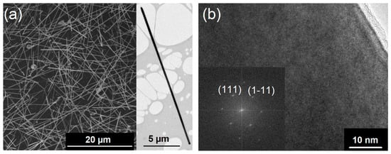
Figure 1.
(a) The SEM image of Si1−xGex NWs grown at 773 K on Au-coated sapphire substrates shows a high number of very long NWs (>20 μm). The TEM image in the inset illustrates the low tendency for tapering of the NWs under these growth conditions. (b) A high-resolution TEM image shows the single crystalline nature of the NWs and the corresponding FFT verifies the growth of the Si1−xGex crystal along the ⟨111⟩ axis.
High-resolution transmission electron microscopy (HR-TEM) images, as shown in Figure 1b, reveal the formation of Si1−xGex single crystals. Moreover, the fast Fourier transform (FFT) of the HR-TEM image in Figure 1b shows the crystal growth along the ⟨111⟩-axis, as expected for group IV NWs of these diameters [58]. Typically, a thin amorphous shell is observed, which is caused by a simultaneous layer formation of amorphous Si1−xGex and the crystalline NW. However, the metal-supported NW growth is much more efficient than an amorphous layer formation at such low growth temperatures of 773 K as described herein.
The Si1−xGex NWs composition was determined by energy dispersive X-ray (EDX) spectroscopy. Figure 2a reveals that the NWs contain a ~1.5–1.3:1 ratio of Si/Ge instead of the predefined ratio of 2:1 in the (H3Si)2Ge(nBu) precursor. This suggests a variation in the decomposition path in the Au-assisted growth, as the Si/Ge ratio is retained in the CVD growth of amorphous layers from the same precursor [51]. Scrambling reactions on the Au surface leading to volatile Si-containing fragments could rationalize the loss of Si. The slow film formation from the same precursor at 773 K in absence of Au causes a thin, negligible overlayer of amorphous Si2Ge. In proximity of the growth seed, no Au has been reliably recorded, but the Au content on the surface of NWs increases over the length of several micrometers, as illustrated in Figure 2a.
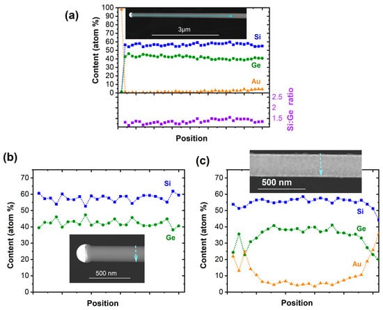
Figure 2.
(a) Elemental distribution of Si, Ge, and Au as well as Si/Ge ratio along the NWs’ axis. The EDX line scan perpendicular to the NW growth axis in (b) shows the group IV elemental distribution of the NW in proximity to the growth seed where no Au has been recorded. (c) The formation of a Si1−xGex/Au core–shell NW towards the NW base is illustrated in the EDX line scan perpendicular to the NW growth axis.
The cross-sectional EDX line scan in proximity to the growth seed shows no Au surface coverage and the formation of a homogeneous material. In agreement with the observation of a significant Au content along the NW, a cross-sectional EDX line scan closer to the NW base illustrates the surface accumulation of Au and the formation of a Si1−xGex/Au core–shell structure (Figure 2c). The minor change in the NWs’ diameter over the length of several micrometers suggests that the Au diffuses along the NWs from the substrate surface that acts as the reservoir, while the Au content along the wire appears to be constant, as illustrated in Figure S1 (Supplementary Material). Moreover, a loss of Au from the growth seed would lead to a significant tapering of the NWs, which is not observed herein. The Au-containing shell is accompanied by slight roughening of the surface, as illustrated in Figure S1. The roughness of the surface and comparably low number of NWs originating from a 5 nm Au film suggest only limited activation of Au growth seeds in the initial stage. As a consequence, the Au is covered with a thin film, preventing further nucleation of NWs. The density of NWs is higher with the increasing growth temperature, but at the same time, an amorphous Si1−xGex-containing shell forms as a result of the competing thin film growth, as discussed below. It should be noted that the Z-contrast within the tips illustrated in the inset of Figure 2b is caused by the high solubility of the group IV semiconductors in Au at a growth temperature of 773 K and the associated phase separation and further growth of the semiconductor segment upon cooling.
As the CVD is carried out at the lowest decomposition temperatures for (H3Si)2Ge(nBu) fragmentation, and thus in the reaction limited regime, a small increase in the substrate temperature will favor the simultaneous formation of an amorphous Si2GeC0.1 layer (Figure S2, Supplementary Material). The consequence is tapering due to the formation of an amorphous Si2GeC0.1 layer, which forms in this temperature regime in absence of Au as a growth promoter [51]. The difference in composition is illustrated in Figure S3 of the Supporting Information with the amorphous layer containing a higher Si content than the inner core. Even though the Au diffusion on the NWs is prevented, the formation of the Si2GeC0.1-based layer would require etching of the amorphous layer while keeping the crystalline core intact, which requires elaborate selective etching. Therefore, the focus is on the Si1−xGex/Au core–shell in the following investigations.
Removal of the Au from the Si1−xGex NWs’ surface using commercial KI/I2 etchant was unsuccessful, which is probably due to partial alloying of Au at the growth temperatures and the formation of a protecting semiconductor-based surface termination [59,60]. Therefore, a harsh thermal dry-oxidation at 1173 K was carried out to oxidize the potential semiconductor shell and subsequently remove the Si1−xGexO2−y by buffered HF. This enabled the Au etching using a commercial KI/I2 solution. The number of longer NWs is lower after the procedure and more fragments are encountered owing to the Au diffusion and agglomeration, leading to segmented NWs as intermediates [61]. However, for Si1−xGex/Au NWs exhibiting mostly surface agglomeration of Au, intact NWs with a rough surface can be obtained that allow for the study of the Si1−xGex NW cores’ electronic properties after the Au removal. Figure S4 (Supplementary Material) shows a TEM image illustrating the rough surface of the obtained Si1−xGex NWs. However, it should be noted that the overall composition of the NW core after this treatment is close to SiGe, showing a preferred etching of Si within the structures. When a Si1−xGex alloy is oxidized, the oxidation potential of Si is sufficiently greater than that of Ge, such that Si is preferentially oxidized and Ge is rejected, which results in a pileup of epitaxial, single-crystal SiGe at the SiO2/Si1−xGex interface [62,63,64]. Therefore, a Ge enrichment is observed in the Si1−xGex NWs presented in this study. A low concentration of Au is not reliably determined by the EDX investigations, but the electronic properties provide a reliable insight into the material’s physical properties, and thus the potential presence of small metal concentrations.
In addition to the TEM/EDX analyses, μ-Raman spectroscopy was carried out on Si1−xGex NWs in order to obtain additional information on the bonding in the substitutional solid solution. Typically, three dominant peaks centered near 300, 400, and 500 cm−1 are considered for Ge–Ge, Ge–Si, and Si–Si stretching motions, respectively. The origin of these peaks in Si1−xGex is well understood [65] and the appearance of the two weak features between 420 and 455 cm−1 as well as the shoulder at the low-frequency side of the Si−Si band is regularly observed [66,67]. All Raman spectra herein are shifted vertically for clarity, while the general intensity depends on the number of wires under focus and will vary. Figure 3 shows the typical signals for Si1−xGex for the as-grown NWs as well as the heat-treated and etched NWs, with the only difference being a slight shift in the Raman peak position associated with the Si−Si mode. The Si−Si band position is the most sensitive to the Ge concentration (x) and downshifts rapidly with increasing x, while the other two bands are not effected significantly by changes in the composition [67]. The general peak location for the as-grown sample with a peak maximum at 488 cm−1 agrees well with literature reports for ~Si0.6Ge0.4 [67] and the aforementioned Si/Ge ratio for the core material being ~1.5–1.3:1, as determined by EDX. However, the Si/Ge ratio of ~1:1 in the annealed and etched NWs according to EDX does not agree with a small shift in the Raman peak position to 492 cm−1, which would be a signature for an increased Si content. Such discrepancies have also been observed in the literature and have been related to either inhomogeneity within batches of NWs or effects of growth temperatures [67].
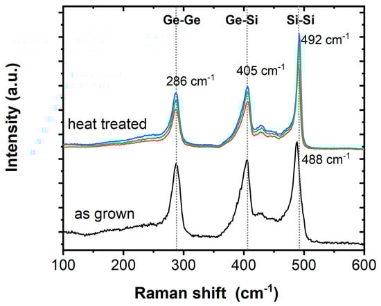
Figure 3.
Raman spectra of as-grown Si1−xGex/Au NWs and Si1−xGex NWs after high-temperature oxidation, annealing, and etching (abbreviated by heat treated).
The electrical characteristics of both Si1−xGex/Au NWs and Si1−xGex NWs were systematically investigated. Thereto, samples of both NW types were transferred to oxidized, highly p-doped Si substrates. Using a combination of electron-beam lithography, sputter deposition of Al, and lift-off techniques, the NWs were integrated into back-gated Schottky barrier FETs with the Si wafer acting as a common back-gate [68]. In total, for both types of NWs, 19 devices each were fabricated. Figure 4a shows representative I/V measurements of both NW types for grounding the Si substrate (VBG = 0 V). Comparing the I/V characteristics, it is evident that the Si1−xGex/Au NWs show an approximately six orders of magnitude higher current than the Si1−xGex NWs. This high conductivity indicates that the main part of the current is flowing through the Au shell of the Si1−xGex/Au NWs rather than the much more resistive Si1−xGex core. Further, Figure 4b shows the investigation of the charge carrier modulation capability by the back-gate on both NWs. Applying a bias voltage of VD = 250 mV, a constant transfer characteristic was observed for the NWs with an Au shell, which screens the electric field of the back-gate, resulting in no gate tunability. On the other hand, the NWs without an Au shell showed typical charge carrier modulation capabilities, i.e., a slightly ambipolar characteristic with dominant hole conduction, as expected for an intrinsic Si1−xGex semiconductor with Al contacts [15,69]. To further map the gate-tunable transport through the proposed NWs, Figure 4c,d show color plots of the recorded current density depending on the applied bias- and gate-voltage. The Si1−xGex/Au NWs reveal a highly symmetric and gate-independent characteristic. In contrast, the Si1−xGex NWs show a typical slightly asymmetric I/V characteristic and charge carrier modulation capability by the back-gate voltage [70].
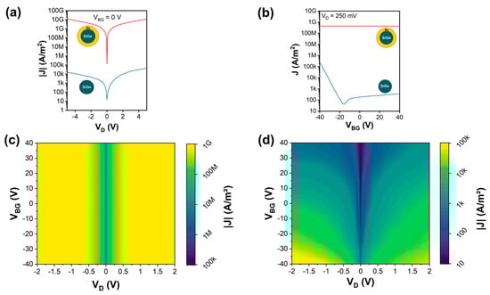
Figure 4.
Electrical characterization of as-grown Si1−xGex/Au NWs and Si1−xGex NWs: (a) current density measurements for VBG = 0 V and sweeping VD from −5 to 5 V; (b) transfer characteristic for VD = 250 mV and respective color maps for (c) Si1−xGex/Au NWs and (d) Si1−xGex NWs.
Importantly, the conducted electrical measurements confirm the results from the structural analysis and illustrate that the presented growth grants access to intrinsic Si1−xGex NWs, which are of high interest for numerous applications in nano- and quantum-electronics [15,23].
4. Conclusions
The Au-assisted synthesis of Si1−xGex NWs was achieved for the first time using a single molecular source as a precursor. In contrast to amorphous layer deposition using (H3Si)2Ge(nBu)2 with retention of the 2:1 Si/Ge ratio, the Au-supported growth leads to Si loss and, typically, a Si/Ge ratio of ~1.5–1.3:1. At higher deposition temperatures, an amorphous layer deposition is observed with the previously reported composition and the overall formation of tapered NWs. Generally, the as-grown NWs are Si1−xGex/Au core–shell structures and formed by Au surface diffusion from the substrate. The Au shell was successfully removed by an oxidation/etching procedure. The electrical properties reveal typical metallic transfer characteristics for Si1−xGex/Au NWs, while the Si1−xGex NWs behave like an intrinsic semiconductor material, as expected. This report demonstrates that highly crystalline Si1−xGex material with typical semiconductor properties can be prepared by the single-source precursor approach.
Supplementary Materials
The following supporting information can be downloaded at https://www.mdpi.com/article/10.3390/nano13040627/s1, Figure S1: EDX and TEM images of Si1−xGex/Au core–shell NWs; Figure S2: TEM images of tapered Si1−xGex NWs; Figure S3: TEM image and EDX analyses across NWs on thicker and thinner parts of tapered Si1−xGex NWs; Figure S4: TEM image of heat-treated and etched Si1−xGex NWs.
Author Contributions
Conceptualization, M.S. and S.B.; methodology, R.B., M.S. and S.B.; validation, R.B., M.S.S., M.S. and S.B.; formal analysis, R.B., M.S.S., M.S. and S.B.; investigation, R.B., V.K., M.S.S., B.K., M.S. and S.B.; resources, K.A.D., M.W., M.S. and S.B.; data curation, R.B., V.K., M.S.S., M.S. and S.B.; writing—original draft preparation, R.B. and S.B.; writing—review and editing, R.B., V.K., M.S.S., B.K., K.A.D., M.W., M.S. and S.B.; supervision, K.A.D., M.W. and S.B.; project administration, M.S. and S.B.; funding acquisition, K.A.D., M.W. and S.B. All authors have read and agreed to the published version of the manuscript.
Funding
This research was funded by the Deutsche Forschungsgemeinschaft (DFG, German Research Foundation) grant numbers: BA6595/1-1 and BA6595/4-1. In addition, the research was funded by the Austrian Science Fund (FWF) project No.: I 5383-N. K.A.D. acknowledges financial support by the Knut and Alice Wallenberg Foundation.
Institutional Review Board Statement
Not applicable.
Data Availability Statement
Data presented in this study are available on request from the corresponding author.
Acknowledgments
S.B. thanks A. Terfort and M. Huth for their support at Goethe University Frankfurt. B.K. and M.W. are grateful to Evonik Operations GmbH, Rheinfelden (Germany), for the generous donation of Si2Cl6 and GeCl4. Open Access Funding by the Austrian Science Fund (FWF).
Conflicts of Interest
The authors declare no conflict of interest.
References
- Jia, C.; Lin, Z.; Huang, Y.; Duan, X. Nanowire Electronics: From Nanoscale to Macroscale. Chem. Rev. 2019, 119, 9074–9135. [Google Scholar] [CrossRef]
- Hrachowina, L.; Chen, Y.; Barrigón, E.; Wallenberg, R.; Borgström, M.T. Realization of axially defined GaInP/InP/InAsP triple-junction photovoltaic nanowires for high-performance solar cells. Mater. Today Energy 2022, 27, 101050. [Google Scholar] [CrossRef]
- Fedeli, J.M.; Nicoletti, S. Mid-Infrared (Mid-IR) Silicon-Based Photonics. Proc. IEEE 2018, 106, 2302–2312. [Google Scholar] [CrossRef]
- Li, Y.; Wang, G.; Akbari-Saatlu, M.; Procek, M.; Radamson, H.H. Si and SiGe Nanowire for Micro-Thermoelectric Generator: A Review of the Current State of the Art. Front. Mater. 2021, 8, 611078. [Google Scholar] [CrossRef]
- Lee, E.K.; Yin, L.; Lee, Y.; Lee, J.W.; Lee, S.J.; Lee, J.; Cha, S.N.; Whang, D.; Hwang, G.S.; Hippalgaonkar, K.; et al. Large Thermoelectric Figure-of-Merits from SiGe Nanowires by Simultaneously Measuring Electrical and Thermal Transport Properties. Nano Lett. 2012, 12, 2918–2923. [Google Scholar] [CrossRef] [PubMed]
- Stokes, K.; Geaney, H.; Flynn, G.; Sheehan, M.; Kennedy, T.; Ryan, K.M. Direct Synthesis of Alloyed Si1−xGex Nanowires for Performance-Tunable Lithium Ion Battery Anodes. ACS Nano 2017, 11, 10088–10096. [Google Scholar] [CrossRef]
- Özgün, A.; Garipcan, B. Silicon nanowires in biomedicine. In Silicon Nanomaterials Sourcebook; Sattler, K.D., Ed.; CRC Press: Boca Raton, FL, USA, 2017. [Google Scholar]
- Güniat, L.; Caroff, P.; Fontcuberta i Morral, A. Vapor Phase Growth of Semiconductor Nanowires: Key Developments and Open Questions. Chem. Rev. 2019, 119, 8958–8971. [Google Scholar] [CrossRef] [PubMed]
- Yang, Y.; Yuan, W.; Kang, W.; Ye, Y.; Pan, Q.; Zhang, X.; Ke, Y.; Wang, C.; Qiu, Z.; Tang, Y. A review on silicon nanowire-based anodes for next-generation high-performance lithium-ion batteries from a material-based perspective. Sustain. Energy Fuels 2020, 4, 1577–1594. [Google Scholar] [CrossRef]
- Amato, M.; Palummo, M.; Rurali, R.; Ossicini, S. Silicon–Germanium Nanowires: Chemistry and Physics in Play, from Basic Principles to Advanced Applications. Chem. Rev. 2014, 114, 1371–1412. [Google Scholar] [CrossRef] [PubMed]
- Barth, S.; Hernandez-Ramirez, F.; Holmes, J.D.; Romano-Rodriguez, A. Synthesis and applications of one-dimensional semiconductors. Prog. Mater. Sci. 2010, 55, 563–627. [Google Scholar] [CrossRef]
- Schmidt, V.; Wittemann, J.V.; Gösele, U. Growth, Thermodynamics, and Electrical Properties of Silicon Nanowires. Chem. Rev. 2010, 110, 361–388. [Google Scholar] [CrossRef] [PubMed]
- Barth, S.; Seifner, M.S.; Maldonado, S. Metastable Group IV Allotropes and Solid Solutions: Nanoparticles and Nanowires. Chem. Mater. 2020, 32, 2703–2741. [Google Scholar] [CrossRef]
- Singh, N.; Buddharaju, K.D.; Manhas, S.K.; Agarwal, A.; Rustagi, S.C.; Lo, G.Q.; Balasubramanian, N.; Kwong, D.L. Si, SiGe Nanowire Devices by Top–Down Technology and Their Applications. IEEE Trans. Electron Devices 2008, 55, 3107–3118. [Google Scholar] [CrossRef]
- Harame, D.; Buquet, J.; Caymax, M.; Cressler, J.; Koester, S.; Masini, G.; Mijazaki, S.; Reznicek, A.; Rim, K.; Takagi, S.; et al. SiGe, Ge, and Related Compounds: Materials, Processing, and Devices; Electrochemical Society (ECS): Pennington, NJ, USA, 2008; Volume 16. [Google Scholar]
- Olesinski, R.W.; Abbaschian, G.J. The Ge–Si (Germanium-Silicon) system. Bull. Alloy Phase Diagr. 1984, 5, 180–183. [Google Scholar] [CrossRef]
- Aberl, J.; Brehm, M.; Fromherz, T.; Schuster, J.; Frigerio, J.; Rauter, P. SiGe quantum well infrared photodetectors on strained-silicon-on-insulator. Opt. Express 2019, 27, 32009–32018. [Google Scholar] [CrossRef]
- Wang, G.L.; Moeen, M.; Abedin, A.; Kolahdouz, M.; Luo, J.; Qin, C.L.; Zhu, H.L.; Yan, J.; Yin, H.Z.; Li, J.F.; et al. Optimization of SiGe selective epitaxy for source/drain engineering in 22 nm node complementary metal-oxide semiconductor (CMOS). J. Appl. Phys. 2013, 114, 123511. [Google Scholar] [CrossRef]
- Marris-Morini, D.; Vakarin, V.; Ramirez, J.M.; Liu, Q.; Ballabio, A.; Frigerio, J.; Montesinos, M.; Alonso-Ramos, C.; Roux, X.L.; Serna, S.; et al. Germanium-based integrated photonics from near- to mid-infrared applications. Nanophotonics 2018, 7, 1781–1793. [Google Scholar] [CrossRef]
- Vakarin, V.; Ye, W.N.; Ramírez, J.M.; Liu, Q.; Frigerio, J.; Ballabio, A.; Isella, G.; Vivien, L.; Alonso-Ramos, C.; Cheben, P.; et al. Ultra-wideband Ge-rich silicon germanium mid-infrared polarization rotator with mode hybridization flattening. Opt. Express 2019, 27, 9838–9847. [Google Scholar] [CrossRef]
- Mheen, B.; Song, Y.-J.; Kang, J.-Y.; Hong, S. Strained-SiGe Complementary MOSFETs Adopting Different Thicknesses of Silicon Cap Layers for Low Power and High Performance Applications. ETRI J. 2005, 27, 439–445. [Google Scholar] [CrossRef]
- Sedky, S.; Witvrouw, A.; Baert, K. Poly SiGe, a promising material for MEMS monolithic integration with the driving electronics. Sens. Actuators A 2002, 97–98, 503–511. [Google Scholar] [CrossRef]
- Scappucci, G.; Kloeffel, C.; Zwanenburg, F.A.; Loss, D.; Myronov, M.; Zhang, J.-J.; De Franceschi, S.; Katsaros, G.; Veldhorst, M. The germanium quantum information route. Nat. Rev. Mater. 2021, 6, 926–943. [Google Scholar] [CrossRef]
- Cecchi, S.; Gatti, E.; Chrastina, D.; Frigerio, J.; Gubler, E.M.; Paul, D.J.; Guzzi, M.; Isella, G. Thin SiGe virtual substrates for Ge heterostructures integration on silicon. J. Appl. Phys. 2014, 115, 093502. [Google Scholar] [CrossRef]
- Li, Y.S.; Sookchoo, P.; Cui, X.; Mohr, R.; Savage, D.E.; Foote, R.H.; Jacobson, R.B.; Sánchez-Pérez, J.R.; Paskiewicz, D.M.; Wu, X.; et al. Electronic Transport Properties of Epitaxial Si/SiGe Heterostructures Grown on Single-Crystal SiGe Nanomembranes. ACS Nano 2015, 9, 4891–4899. [Google Scholar] [CrossRef] [PubMed]
- Pillarisetty, R.; Chu-Kung, B.; Corcoran, S.; Dewey, G.; Kavalieros, J.; Kennel, H.; Kotlyar, R.; Le, V.; Lionberger, D.; Metz, M.; et al. High mobility strained germanium quantum well field effect transistor as the p-channel device option for low power (Vcc = 0.5 V) III–V CMOS architecture. In Proceedings of the 2010 International Electron Devices Meeting, San Francisco, CA, USA, 6–8 December 2010; pp. 6.7.1–6.7.4. [Google Scholar]
- Terashima, K.; Tajima, M.; Tatsumi, T. Near-band-gap photoluminescence of Si1−xGex alloys grown on Si(100) by molecular beam epitaxy. Appl. Phys. Lett. 1990, 57, 1925–1927. [Google Scholar] [CrossRef]
- Sturm, J.C.; Manoharan, H.; Lenchyshyn, L.C.; Thewalt, M.L.W.; Rowell, N.L.; Noël, J.P.; Houghton, D.C. Well-resolved band-edge photoluminescence of excitons confined in strained Si1−xGex quantum wells. Phys. Rev. Lett. 1991, 66, 1362–1365. [Google Scholar] [CrossRef]
- Ashburn, P.; Bagnall, D. Silicon–Germanium: Properties, Growth and Applications. In Springer Handbook of Electronic and Photonic Materials; Kasap, S., Capper, P., Eds.; Springer: Boston, MA, USA, 2007; pp. 481–498. [Google Scholar]
- Oehme, M.; Werner, J.; Kirfel, O.; Kasper, E. MBE growth of SiGe with high Ge content for optical applications. Appl. Surf. Sci. 2008, 254, 6238–6241. [Google Scholar] [CrossRef]
- Kuan, T.S.; Iyer, S.S. Strain relaxation and ordering in SiGe layers grown on (100), (111), and (110) Si surfaces by molecular-beam epitaxy. Appl. Phys. Lett. 1991, 59, 2242–2244. [Google Scholar] [CrossRef]
- Alam, M.M.; Wagatsuma, Y.; Okada, K.; Hoshi, Y.; Yamada, M.; Hamaya, K.; Sawano, K. Critical thickness of strained Si1−xGex on Ge(111) and Ge-on-Si(111). Appl. Phys. Express 2019, 12, 081005. [Google Scholar] [CrossRef]
- Maydell, K.V.; Grunewald, K.; Kellermann, M.; Sergeev, O.; Klement, P.; Reininghaus, N.; Kilper, T. Microcrystalline SiGe Absorber Layers in Thin-film Silicon Solar Cells. Energy Procedia 2014, 44, 209–215. [Google Scholar] [CrossRef]
- Capellini, G.; Seta, M.D.; Busby, Y.; Pea, M.; Evangelisti, F.; Nicotra, G.; Spinella, C.; Nardone, M.; Ferrari, C. Strain relaxation in high Ge content SiGe layers deposited on Si. J. Appl. Phys. 2010, 107, 063504. [Google Scholar] [CrossRef]
- Qi, C.; Goncher, G.; Solanki, R.; Jordan, J. SiGe nanowire growth and characterization. Nanotechnology 2007, 18, 075302. [Google Scholar] [CrossRef]
- Potié, A.; Baron, T.; Latu-Romain, L.; Rosaz, G.; Salem, B.; Montès, L.; Gentile, P.; Kreisel, J.; Roussel, H. Controlled growth of SiGe nanowires by addition of HCl in the gas phase. J. Appl. Phys. 2011, 110, 024311. [Google Scholar] [CrossRef]
- Lew, K.-K.; Pan, L.; Dickey, E.C.; Redwing, J.M. Vapor–Liquid–Solid Growth of Silicon–Germanium Nanowires. Adv. Mater. 2003, 15, 2073–2076. [Google Scholar] [CrossRef]
- Hsu, Y.-J.; Lu, S.-Y.; Lin, Y.-F. One-Step Preparation of Coaxial CdS–ZnS and Cd1−xZnxS–ZnS Nanowires. Adv. Funct. Mater. 2005, 15, 1350–1357. [Google Scholar] [CrossRef]
- Akhtar, J.; Akhtar, M.; Malik, M.A.; O’Brien, P.; Raftery, J. A Single-Source Precursor Route to Unusual PbSe Nanostructures by a Solution–Liquid–Solid Method. J. Am. Chem. Soc. 2012, 134, 2485–2487. [Google Scholar] [CrossRef] [PubMed]
- Mathur, S.; Barth, S. Molecule-Based Chemical Vapor Growth of Aligned SnO2 Nanowires and Branched SnO2/V2O5 Heterostructures. Small 2007, 3, 2070–2075. [Google Scholar] [CrossRef]
- Sardar, K.; Dan, M.; Schwenzer, B.; Rao, C.N.R. A simple single-source precursor route to the nanostructures of AlN, GaN and InN. J. Mater. Chem. 2005, 15, 2175–2177. [Google Scholar] [CrossRef]
- Lobreyer, T.; Oberhammer, H.; Sundermeyer, W. Synthesis and Structure of Tetrasilylgermane, Ge(SiH3)4, and Other Silylgermanes. Angew. Chem. Int. Ed. Engl. 1993, 32, 586–587. [Google Scholar] [CrossRef]
- Hu, C.; Taraci, J.L.; Tolle, J.; Bauer, M.R.; Crozier, P.A.; Tsong, I.S.T.; Kouvetakis, J. Synthesis of Highly Coherent SiGe and Si4Ge Nanostructures by Molecular Beam Epitaxy of H3SiGeH3 and Ge(SiH3)4. Chem. Mater. 2003, 15, 3569–3572. [Google Scholar] [CrossRef]
- Lee, M.-S.; Bent, S.F. Bonding and Thermal Reactivity in Thin a-SiC:H Films Grown by Methylsilane CVD. J. Phys. Chem. B 1997, 101, 9195–9205. [Google Scholar] [CrossRef]
- Liu, C.W.; Sturm, J.C. Low temperature chemical vapor deposition growth of β-SiC on (100) Si using methylsilane and device characteristics. J. Appl. Phys. 1997, 82, 4558–4565. [Google Scholar] [CrossRef]
- Johnson, A.D.; Perrin, J.; Mucha, J.A.; Ibbotson, D.E. Kinetics of silicon carbide CVD: Surface decomposition of silacyclobutane and methylsilane. J. Phys. Chem. 1993, 97, 12937–12948. [Google Scholar] [CrossRef]
- Hewitt, S.B.; Tay, S.-P.; Tarr, N.G.; Boothroyd, A.R. Silicon carbide emitter diodes by LPCVD (low-pressure chemical vapour deposition) using di-tert-butylsilane. Can. J. Phys. 1992, 70, 946–948. [Google Scholar] [CrossRef]
- Poungoué Mbeunmi, A.B.; Arvinte, R.; Pelletier, H.; Jellite, M.; Arès, R.; Fafard, S.; Boucherif, A. Growth of Ge epilayers using iso-butylgermane (IBGe) and its memory effect in an III-V chemical beam epitaxy reactor. J. Cryst. Growth 2020, 547, 125807. [Google Scholar] [CrossRef]
- Jakomin, R.; Beaudoin, G.; Gogneau, N.; Lamare, B.; Largeau, L.; Mauguin, O.; Sagnes, I. p and n-type germanium layers grown using iso-butyl germane in a III-V metal-organic vapor phase epitaxy reactor. Thin Solid Films 2011, 519, 4186–4191. [Google Scholar] [CrossRef]
- Seifner, M.S.; Dijkstra, A.; Bernardi, J.; Steiger-Thirsfeld, A.; Sistani, M.; Lugstein, A.; Haverkort, J.E.M.; Barth, S. Epitaxial Ge0.81Sn0.19 Nanowires for Nanoscale Mid-Infrared Emitters. ACS Nano 2019, 13, 8047–8054. [Google Scholar] [CrossRef] [PubMed]
- Köstler, B.; Jungwirth, F.; Achenbach, L.; Sistani, M.; Bolte, M.; Lerner, H.-W.; Albert, P.; Wagner, M.; Barth, S. Mixed-Substituted Single-Source Precursors for Si1−xGex Thin Film Deposition. Inorg. Chem. 2022, 61, 17248–17255. [Google Scholar] [CrossRef] [PubMed]
- Mathur, S.; Barth, S.; Shen, H. Chemical Vapor Growth of NiGa2O4 Films: Advantages and Limitations of a Single Molecular Source. Chem. Vap. Depos. 2005, 11, 11–16. [Google Scholar] [CrossRef]
- Barth, S.; Seifner, M.S.; Bernardi, J. Growth of monocrystalline In2O3 nanowires by a seed orientation dependent vapour–solid–solid mechanism. J. Mater. Chem. C 2014, 2, 5747–5751. [Google Scholar] [CrossRef]
- Seifner, M.S.; Sistani, M.; Porrati, F.; Di Prima, G.; Pertl, P.; Huth, M.; Lugstein, A.; Barth, S. Direct Synthesis of Hyperdoped Germanium Nanowires. ACS Nano 2018, 12, 1236–1241. [Google Scholar] [CrossRef]
- Wagner, R.S.; Ellis, W.C. Vapor-Liquid-Solid Mechanism of Single Crystal Growth. Appl. Phys. Lett. 1964, 4, 89–90. [Google Scholar] [CrossRef]
- Gamalski, A.D.; Ducati, C.; Hofmann, S. Cyclic Supersaturation and Triple Phase Boundary Dynamics in Germanium Nanowire Growth. J. Phys. Chem. C 2011, 115, 4413–4417. [Google Scholar] [CrossRef]
- Maliakkal, C.B.; Mårtensson, E.K.; Tornberg, M.U.; Jacobsson, D.; Persson, A.R.; Johansson, J.; Wallenberg, L.R.; Dick, K.A. Independent Control of Nucleation and Layer Growth in Nanowires. ACS Nano 2020, 14, 3868–3875. [Google Scholar] [CrossRef] [PubMed]
- Schmidt, V.; Senz, S.; Gösele, U. Diameter-Dependent Growth Direction of Epitaxial Silicon Nanowires. Nano Lett. 2005, 5, 931–935. [Google Scholar] [CrossRef]
- Hessel, C.M.; Heitsch, A.T.; Korgel, B.A. Gold Seed Removal from the Tips of Silicon Nanorods. Nano Lett. 2010, 10, 176–180. [Google Scholar] [CrossRef]
- Puglisi, R.A.; Bongiorno, C.; Borgh, G.; Fazio, E.; Garozzo, C.; Mannino, G.; Neri, F.; Pellegrino, G.; Scalese, S.; La Magna, A. Study on the Physico-Chemical Properties of the Si Nanowires Surface. Nanomaterials 2019, 9, 818. [Google Scholar] [CrossRef] [PubMed]
- Benter, S.; Dubrovskii, V.G.; Bartmann, M.; Campo, A.; Zardo, I.; Sistani, M.; Stöger-Pollach, M.; Lancaster, S.; Detz, H.; Lugstein, A. Quasi One-Dimensional Metal–Semiconductor Heterostructures. Nano Lett. 2019, 19, 3892–3897. [Google Scholar] [CrossRef] [PubMed]
- Margalit, S.; Bar-Lev, A.; Kuper, A.B.; Aharoni, H.; Neugroschel, A. Oxidation of silicon-germanium alloys. J. Cryst. Growth 1972, 17, 288–297. [Google Scholar] [CrossRef]
- LeGoues, F.K.; Rosenberg, R.; Nguyen, T.; Himpsel, F.; Meyerson, B.S. Oxidation studies of SiGe. J. Appl. Phys. 1989, 65, 1724–1728. [Google Scholar] [CrossRef]
- Long, E.; Galeckas, A.; Kuznetsov, A.Y. Ge concentrations in pile-up layers of sub-100-nm SiGe films for nano-structuring by thermal oxidation. J. Vac. Sci. Technol. B 2012, 30, 041212. [Google Scholar] [CrossRef]
- Yu, P.Y.; Cardona, M. Fundamentals of Semiconductors; Springer: Berlin/Heidelberg, Germany, 2010. [Google Scholar]
- Ren, S.-F.; Cheng, W.; Yu, P.Y. Microscopic investigation of phonon modes in SiGe alloy nanocrystals. Phys. Rev. B 2004, 69, 235327. [Google Scholar] [CrossRef]
- Lu, Q.; Adu, K.W.; Gutiérrez, H.R.; Chen, G.; Lew, K.-K.; Nimmatoori, P.; Zhang, X.; Dickey, E.C.; Redwing, J.M.; Eklund, P.C. Raman Scattering from Si1−xGex Alloy Nanowires. J. Phys. Chem. C 2008, 112, 3209–3215. [Google Scholar] [CrossRef]
- Sistani, M.; Staudinger, P.; Greil, J.; Holzbauer, M.; Detz, H.; Bertagnolli, E.; Lugstein, A. Room-Temperature Quantum Ballistic Transport in Monolithic Ultrascaled Al–Ge–Al Nanowire Heterostructures. Nano Lett. 2017, 17, 4556–4561. [Google Scholar] [CrossRef]
- Wind, L.; Sistani, M.; Böckle, R.; Smoliner, J.; Vukŭsić, L.; Aberl, J.; Brehm, M.; Schweizer, P.; Maeder, X.; Michler, J.; et al. Composition Dependent Electrical Transport in Si1−xGex Nanosheets with Monolithic Single-Elementary Al Contacts. Small 2022, 18, 2204178. [Google Scholar] [CrossRef]
- Park, S.J.; Jeon, D.-Y.; Sessi, V.; Trommer, J.; Heinzig, A.; Mikolajick, T.; Kim, G.-T.; Weber, W.M. Channel Length-Dependent Operation of Ambipolar Schottky-Barrier Transistors on a Single Si Nanowire. ACS Appl. Mater. Interfaces 2020, 12, 43927–43932. [Google Scholar] [CrossRef]


Disclaimer/Publisher’s Note: The statements, opinions and data contained in all publications are solely those of the individual author(s) and contributor(s) and not of MDPI and/or the editor(s). MDPI and/or the editor(s) disclaim responsibility for any injury to people or property resulting from any ideas, methods, instructions or products referred to in the content. |
© 2023 by the authors. Licensee MDPI, Basel, Switzerland. This article is an open access article distributed under the terms and conditions of the Creative Commons Attribution (CC BY) license (https://creativecommons.org/licenses/by/4.0/).