
Design and Analysis of Gallium Arsenide-Based Nanowire Using Coupled Non-Equilibrium Green Function for RF Hybrid Applications


Abstract
:1. Introduction
2. Basics of NEGF Modeling
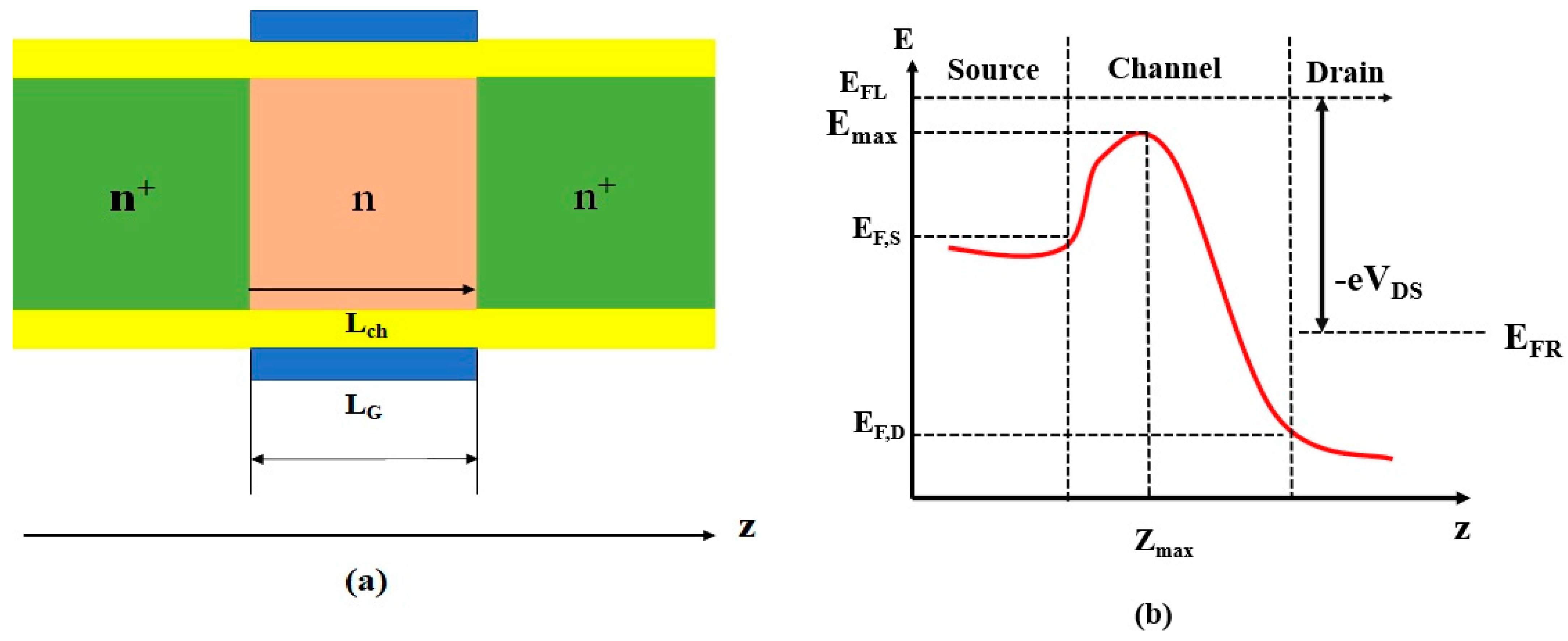
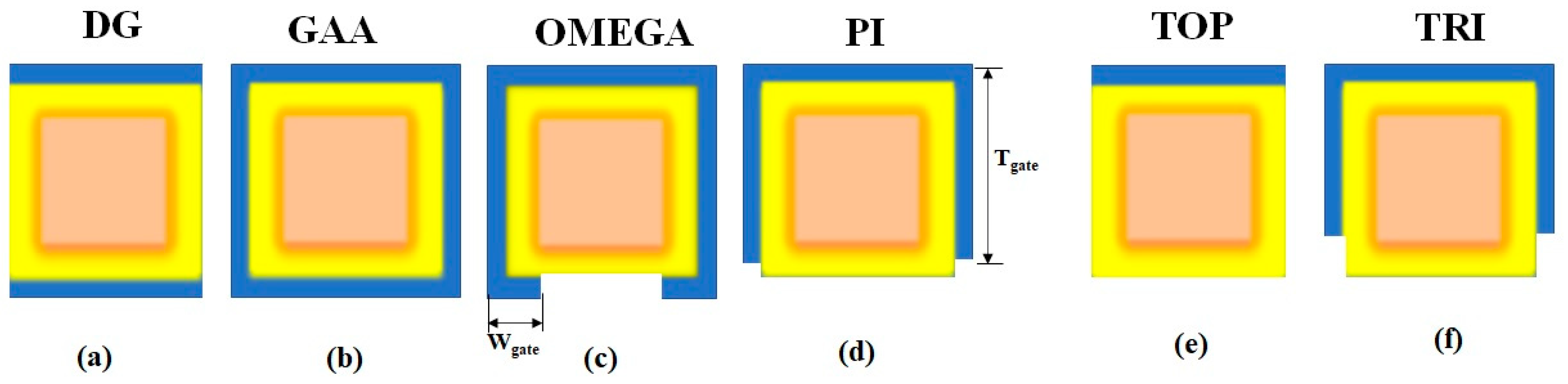
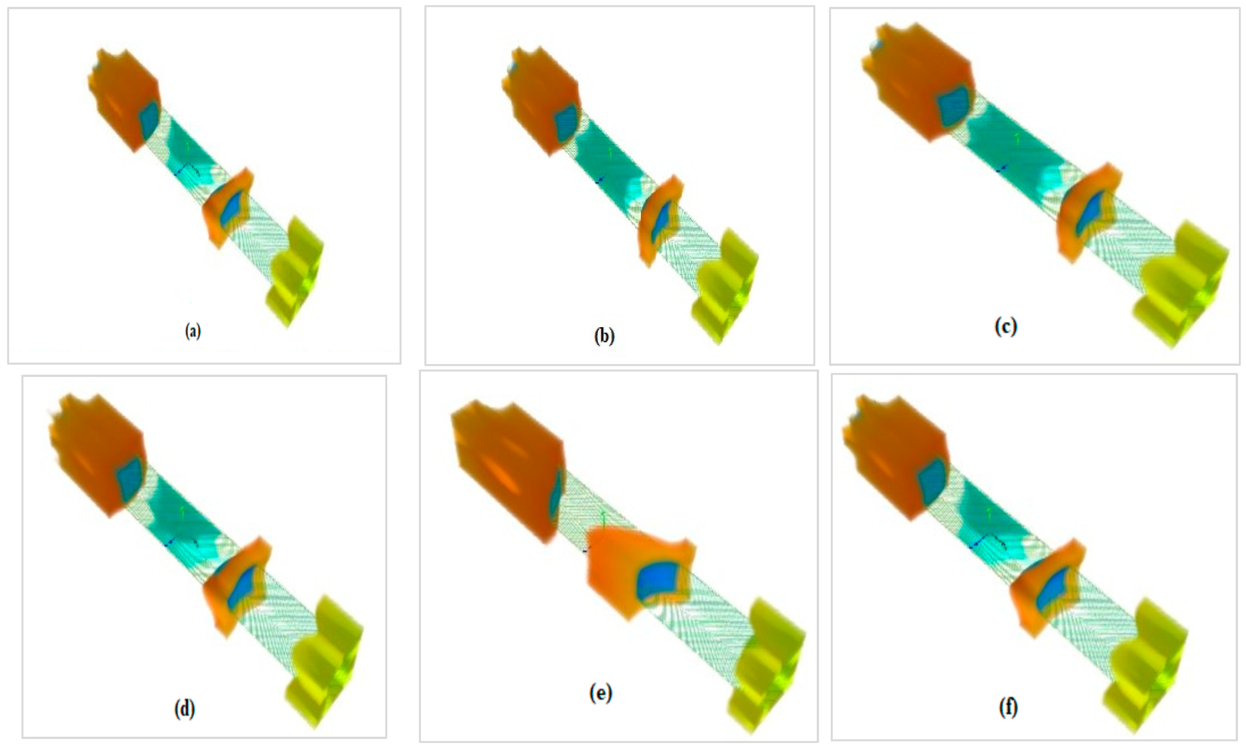
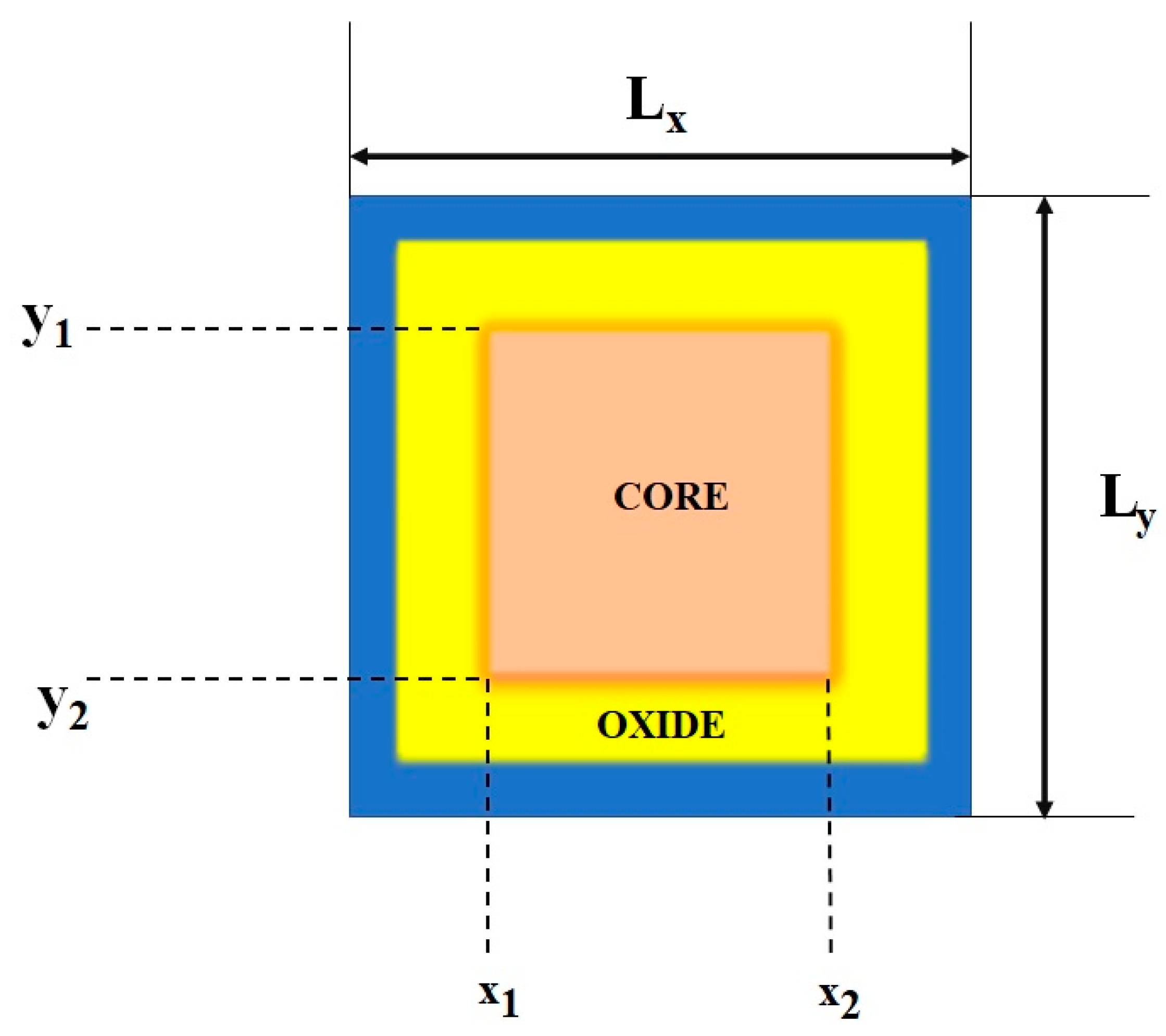
3. Design of Proposed Novel GaAs Nanowire
4. Mathematical Modeling of the Nanowire with La2O3
4.1. Numerical Approaches
4.1.1. K-Space Solutions of Two-Dimensional Schrodinger Equations
4.1.2. Product Space Solutions of 2-D Schrodinger Equations
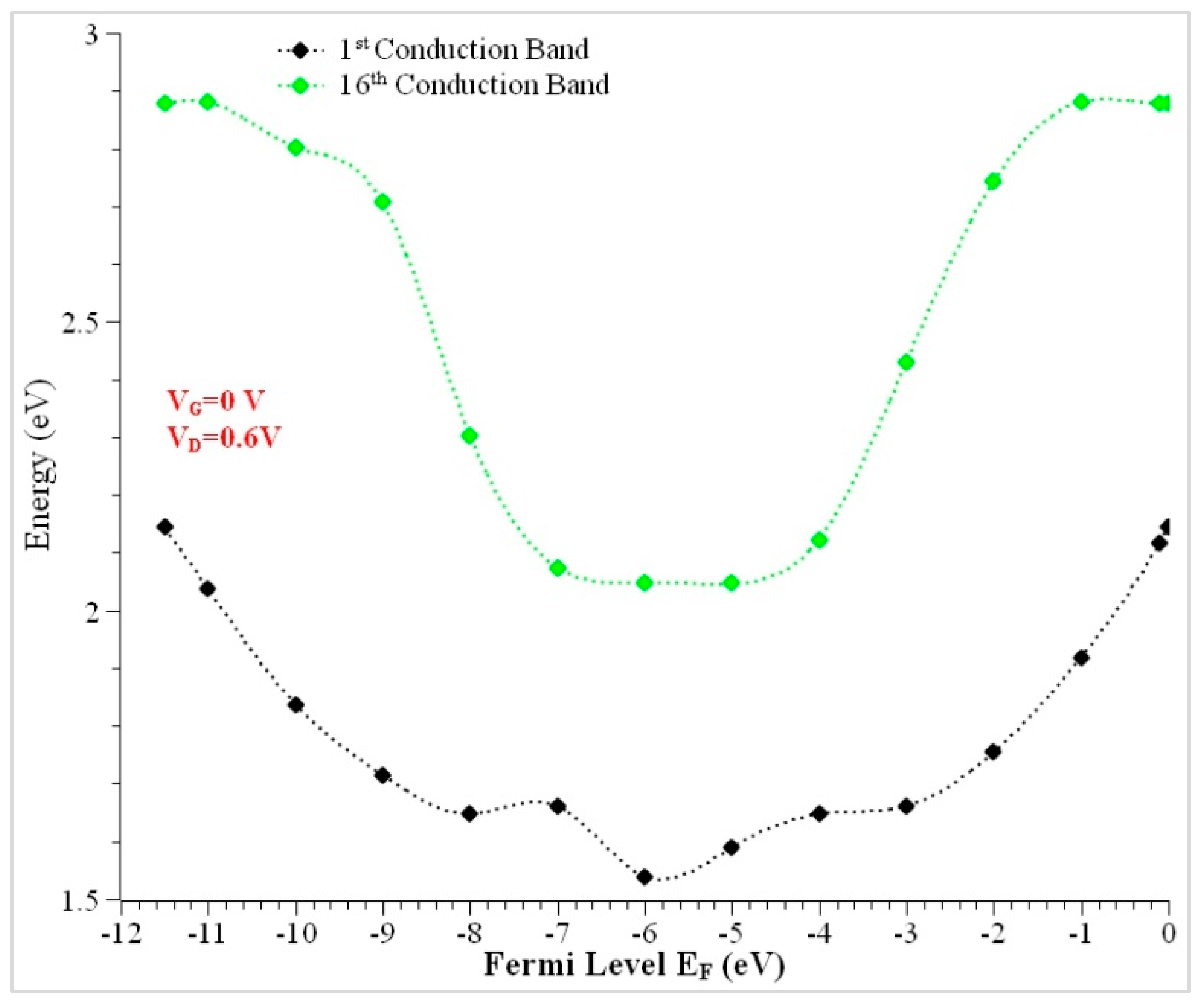
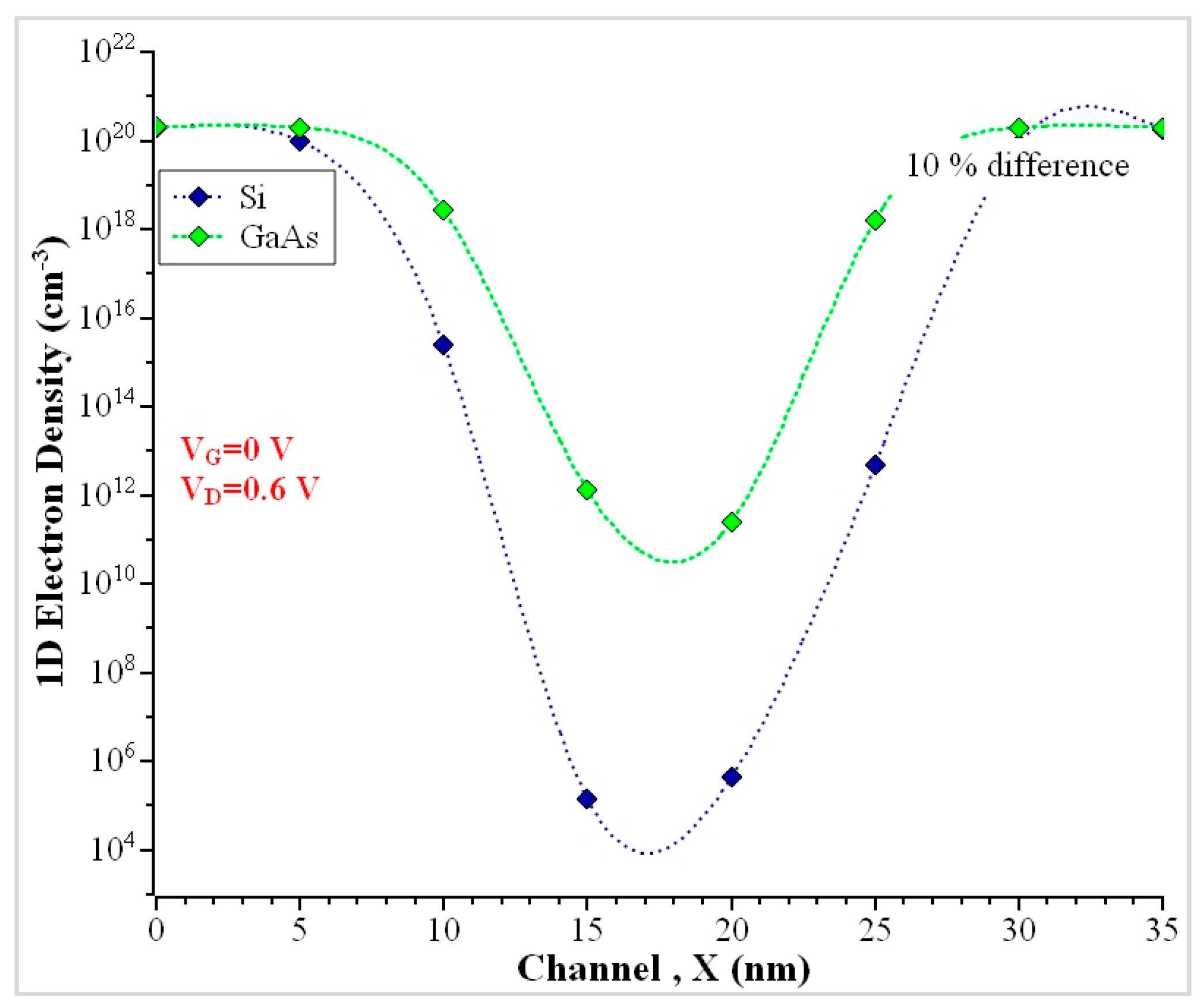
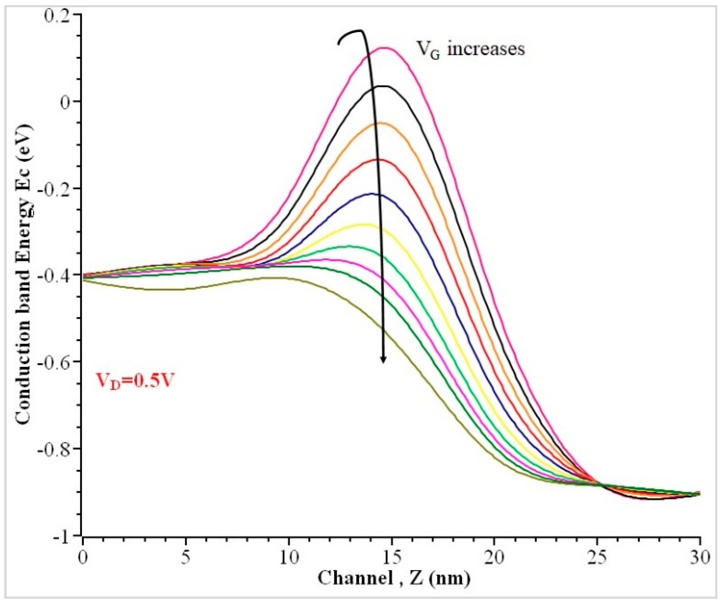
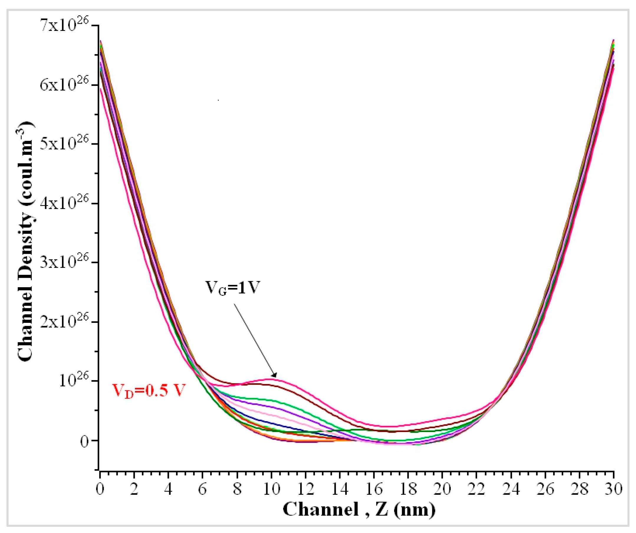
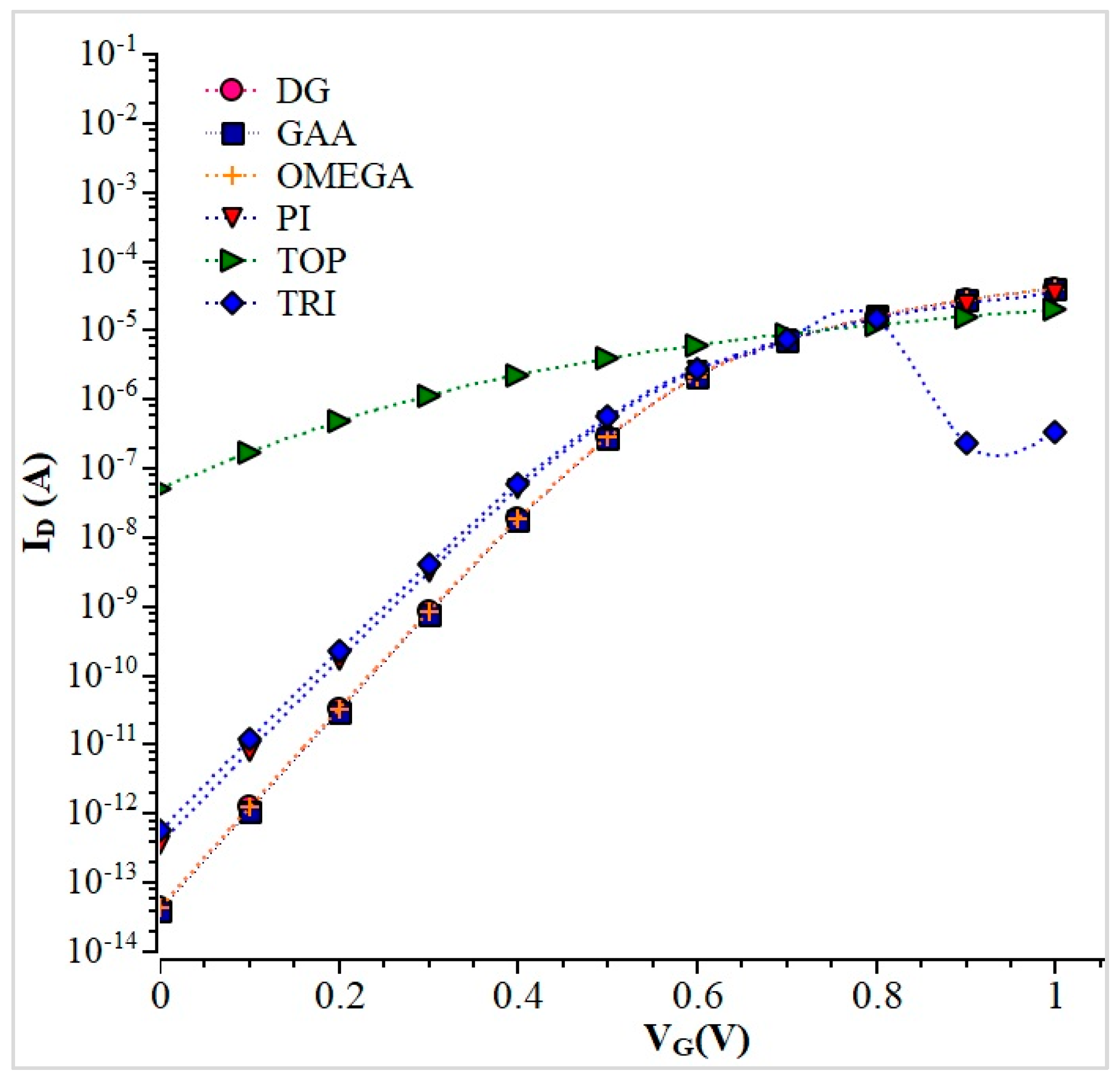
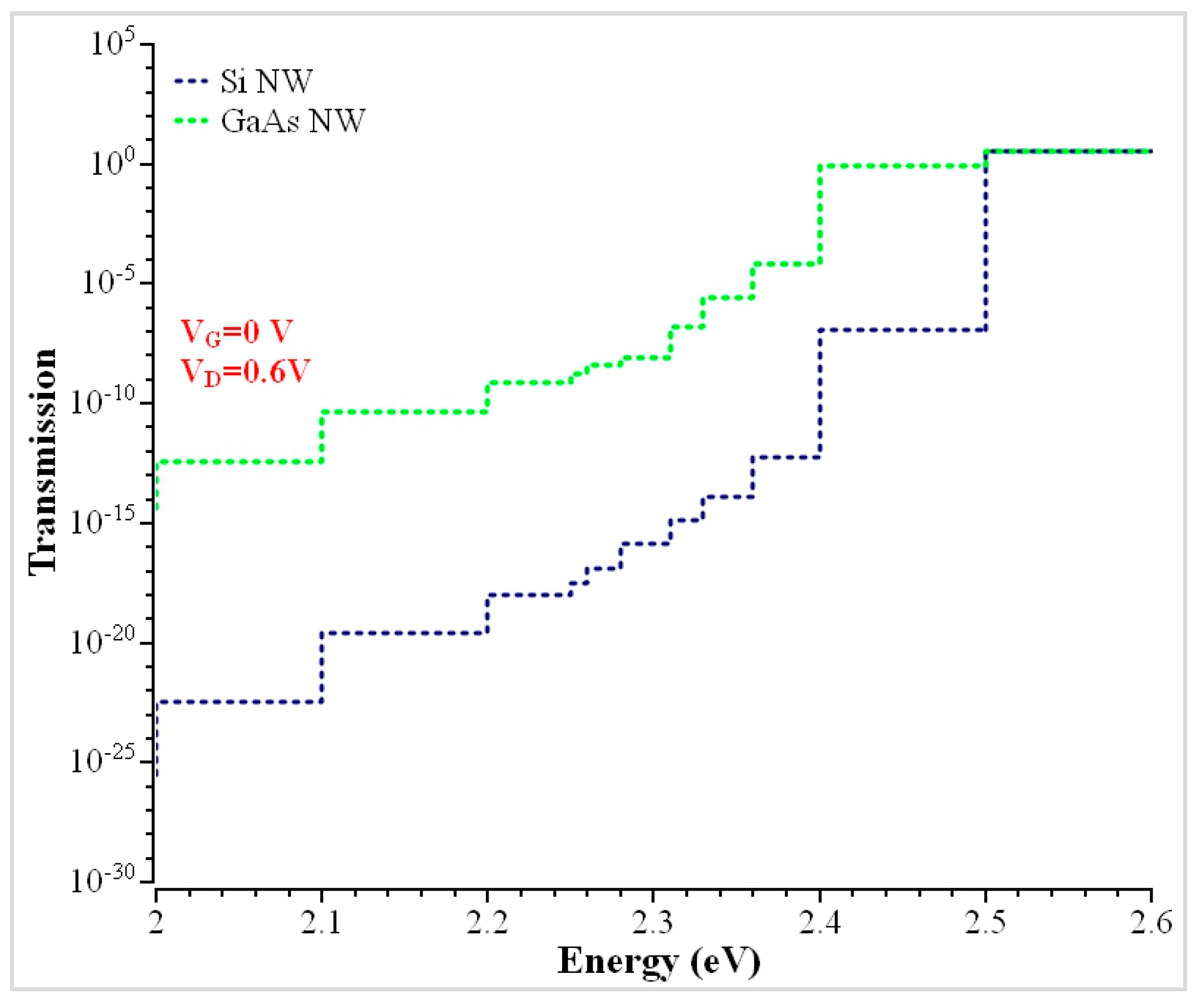
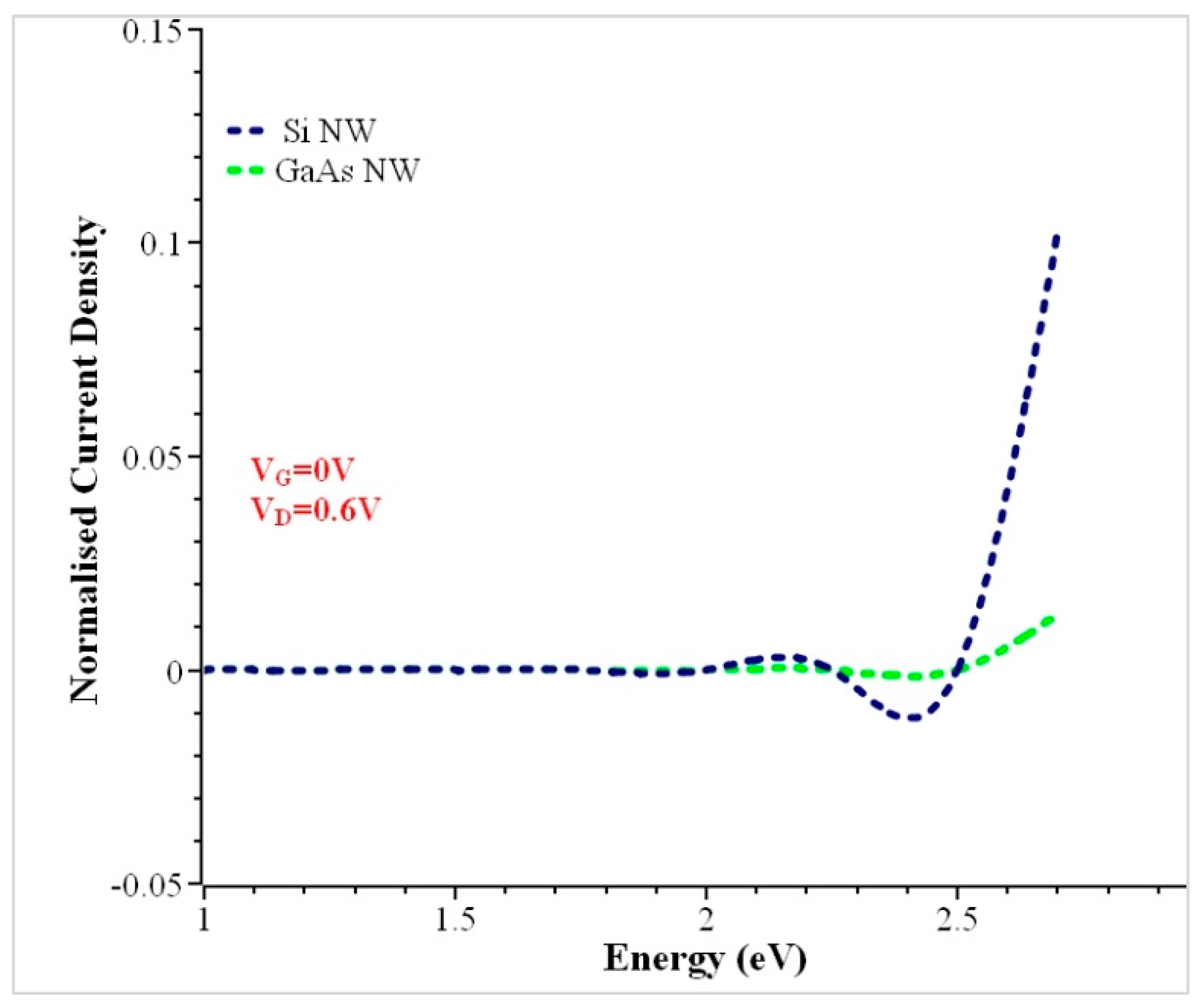
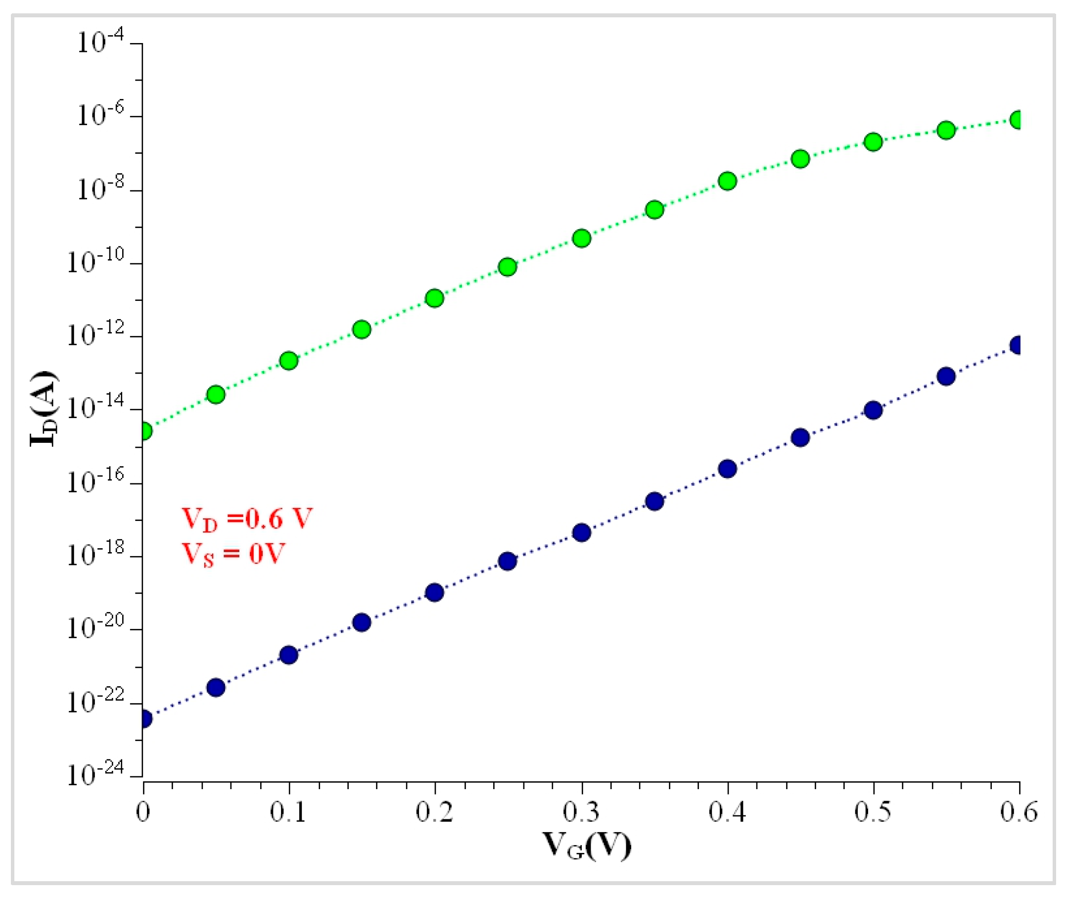
5. Analysis of the GaAs-Based Nanowire
6. Conclusions and Future Recommendations
Author Contributions
Funding
Data Availability Statement
Conflicts of Interest
References
- Colinge, J.P. FinFETs, and Other Multi-Gate Transistors; Springer US: New York, NY, USA, 2008. [Google Scholar]
- Goldberger, J.; Hochbaum, A.I.; Fan, R.; Yang, P. Silicon Vertically Integrated Nanowire Field Effect Transistors. Nano Lett. 2006, 6, 973–977. [Google Scholar]
- Natori, K. Ballistic/quasi-ballistic transport in nanoscale transistor. Appl. Surf. Sci. 2008, 254, 6194–6198. [Google Scholar] [CrossRef] [Green Version]
- Numata, T.; Uno, S.; Hattori, J.; Milnikov, G.; Kamakura, Y.; Mori, N.; Nakazato, K. A Self-Consistent Compact Model of Ballistic Nanowire MOSFET with Rectangular Cross Section. IEEE Trans. Electron Devices 2013, 60, 856–862. [Google Scholar] [CrossRef]
- Batakala, J.; Dhar, R.S. Effect of channel material on the performance parameters of GAA MOSFET. J. Nano Electron. Phys. 2022, 14, 02003. [Google Scholar] [CrossRef]
- Hosseini, R.; Fathipour, M.; Faez, R. A comparative study of NEGF and DDMS models in the GAA silicon nanowire transistor. Int. J. Electron. 2012, 99, 1299–1307. [Google Scholar] [CrossRef]
- Wang, J.; Polizzi, E.; Lundstrom, M. A Three-dimensional Quantum Simulation of Silicon Nanowire Transistors with the Effective-Mass Approximation. J. Appl. Phys. 2004, 96, 2192–2203. [Google Scholar] [CrossRef] [Green Version]
- Samuel, A.; Arumugam, N.; Shenbagavalli, A. Drain current characteristics of silicon nanowire field effect transistor. J. Microelectron. 2016, 2, 284–287. [Google Scholar] [CrossRef]
- Coquand, R.; Barraud, S.; Cass, M.; Leroux, P.; Vizioz, C.; Comboroure, C.; Perreau, P.; Ernst, E.; Samson, M.-P.; Maffini-Alvaro, V.; et al. Scaling of high-/metal-gate TriGate SOI nanowire transistors down to 10 nm width. Solid-State Electron. 2013, 88, 32–36. [Google Scholar] [CrossRef]
- Ramayya, E.B.; Vasileska, D.; Goodnick, S.M.; Knezevic, I. Electron transport in silicon nanowires: The role of acoustic phonon confinement and surface roughness scattering. J. Appl. Phys. 2008, 104, 063711. [Google Scholar] [CrossRef] [Green Version]
- Cresti, A.; Pala, M.G.; Poli, S.; Mouis, M.; Ghibaudo, G. A Comparative Study of Surface-Roughness-Induced Variability in Silicon Nanowire and Double-Gate FETs. IEEE Trans. Electron Devices 2011, 58, 2274–2281. [Google Scholar] [CrossRef]
- Jin, S.; Tang, T.; Fischetti, M.V. Anatomy of Carrier Backscattering in Silicon Nanowire Transistors. In Proceedings of the 2009 13th International Workshop on Computational Electronics, Beijing, China, 27–29 May 2009. [Google Scholar] [CrossRef]
- Dargar, S.K.; Srivastava, V.M. Performance analysis of High-k dielectric-based silicon nanowire gate-all-around tunneling FET. Int. J. Electr. Electron. Eng. Telecommun. 2019, 8, 340–345. [Google Scholar] [CrossRef]
- Srivastava, V.M.; Singh, G. MOSFET Technologies for Double-Pole Four-Throw Radio-Frequency Switch; Analog Circuits and Signal Processing; Springer International Publishing: Cham, Switzerland, 2014. [Google Scholar] [CrossRef]
- Martinez, A.; Seoane, N.; Brown, A.R.; Barker, J.R.; Asenov, A. 3-D Non-equilibrium Green’s Function Simulation of Nonperturbative Scattering from Discrete Dopants in the Source and Drain of a Silicon Nanowire Transistor. IEEE Trans. Nanotechnol. 2009, 8, 603–610. [Google Scholar] [CrossRef] [Green Version]
- Dubrovskii, V.G.; Hijazi, H.; Isik Goktas, N.; LaPierre, R.R. Be, Te and Si Doping of GaAs Nanowires: Theory and Experiment. J. Phys. Chem. C 2020, 124, 17299–17307. [Google Scholar] [CrossRef]
- Asenov, A.; Wang, Y.; Cheng, B.; Wang, X.; Asenov, P.; Al-Ameri, T.; Georgiev, V.P. Nanowire transistor solutions for 5 nm and beyond. In Proceedings of the 2016 17th International Symposium on Quality Electronic Design (ISQED), Santa Clara, CA, USA, 15–16 March 2016. [Google Scholar] [CrossRef] [Green Version]
- Svizhenko, A.; Anantram, M.P.; Govindan, T.R.; Biegel, B.; Venugopal, R. Two-dimensional quantum mechanical modeling of nanotransistors. J. Appl. Phys. 2002, 91, 2343–2354. [Google Scholar] [CrossRef] [Green Version]
- Luisier, M.; Schenk, A.; Fichtner, W. Quantum transport in two- and three-dimensional nanoscale transistors: Coupled mode effects in the non-equilibrium Green’s function formalism. J. Appl. Phys. 2006, 100, 043713. [Google Scholar] [CrossRef] [Green Version]
- Luisier, M.; Schenk, A.; Fichtner, W.; Klimeck, G. Atomistic simulation of nanowires in the sp3d5s* tight-binding formalism: From boundary conditions to strain calculations. Phys. Rev. B 2006, 74, 205323. [Google Scholar] [CrossRef] [Green Version]
- Luisier, M.; Schenk, A.; Fichtner, W.; Klimeck, G. Transport calculation of Semiconductor Nanowires Coupled to Quantum Well Reservoirs. J. Comput. Electron. 2006, 6, 199–202. [Google Scholar] [CrossRef] [Green Version]
- Gueorguiev, G.K.; Stafström, S.; Hultman, L. Nano-wire formation by self-assembly of silicon–metal cage-like molecules. Chem. Phys. Lett. 2008, 458, 170–174. [Google Scholar] [CrossRef]
- Kakanakova-Georgieva, A.; Ivanov, I.G.; Suwannaharn, N.; Hsu, C.-W.; Cora, I.; Pécz, B.; Gueorguiev, G.K. MOCVD of AlN on epitaxial graphene at extreme temperatures. CrystEngComm 2020, 23, 385–390. [Google Scholar] [CrossRef]
- Kumarasinghe, C.; Bowler, D.R. DFT study of undoped and As-doped Si nanowires approaching the bulk limit. J. Phys. Condens. Matter 2019, 32, 035304. [Google Scholar] [CrossRef] [Green Version]
- García-Cristóbal, A.; Molina-Sánchez, A. Tight-Binding Simulations of Nanowires. In Encyclopedia of Nanotechnology; Springer: Dordrecht, The Netherlands, 2015; pp. 1–12. [Google Scholar] [CrossRef]
- Morioka, N.; Yoshioka, H.; Suda, J.; Kimoto, T. Quantum-confinement effect on holes in silicon nanowires: Relationship between wave function and band structure. J. Appl. Phys. 2011, 109, 064318. [Google Scholar] [CrossRef] [Green Version]
- Paramasivam, P.; Gowthaman, N.; Srivastava, V.M. Design and analysis of InP/InAs/AlGaAs based Cylindrical Surrounding Double-Gate (CSDG) MOSFETs with La2O3 for 5-nm technology. IEEE Access 2021, 9, 159566–159576. [Google Scholar] [CrossRef]
- Gowthaman, N.; Srivastava, V.M. Mathematical modeling of drain current estimation in a CSDG MOSFET, based on La2O3 oxide layer with fabrication—A nanomaterial approach. Nanomaterials 2022, 12, 3374. [Google Scholar] [CrossRef]
- Neophytou, N.; Kosina, H. Hole mobility increase in ultra-narrow si channels under strong (110) surface confinement. Appl. Phys. Lett. 2011, 99, 092110. [Google Scholar] [CrossRef] [Green Version]
- Alam, K.; Sajjad, R.N. Electronic Properties and Orientation-Dependent Performance of InAs Nanowire Transistors. IEEE Trans. Electron Devices 2010, 57, 2880–2885. [Google Scholar] [CrossRef]
- Horiguchi, S. Validity of effective mass theory for energy levels in Si quantum wires. Phys. B Condens. Matter 1996, 227, 336–338. [Google Scholar] [CrossRef]
- Datta, S. Nanoscale device modeling: The Greens function method. Superlatt. Microstruct. 2000, 28, 253–278. [Google Scholar] [CrossRef]
- Ren, Z.; Venugopal, R.; Goasguen, S.; Datta, S.; Lundstrom, M.S. nanoMOS 2.5: A two-dimensional simulator for quantum transport in double-gate MOSFETs. IEEE Trans. Electron Devices 2003, 50, 1914–1925. [Google Scholar] [CrossRef]
- Martinez, A.; Barker, J.R. Quantum Transport in a Silicon Nanowire FET Transistor: Hot Electrons and Local Power Dissipation. Materials 2020, 13, 3326. [Google Scholar] [CrossRef]
- Abramo, A.; Cardin, A.; Selmi, L.; Sangiorgi, E. Two-dimensional quantum mechanical simulation of charge distribution in silicon MOSFETs. IEEE Trans. Electron Dev. 2000, 27, 1858–1863. [Google Scholar] [CrossRef]
- Seoane, N.; Martinez, A.; Brown, A.R.; Asenov, A. Study of surface roughness in extremely small Si nanowire MOSFETs using fully-3D NEGFs. In Proceedings of the 2009 Spanish Conference on Electron Devices, Santiago de Compostela, Spain, 11–13 February 2009. [Google Scholar] [CrossRef]
- Al Mamun Mazumdar, A.; Hosen, K.; Islam, M.S.; Park, J. Numerical investigations of nanowire gate-all-around negative capacitance GaAs/InN tunnel FET. Digit. Object Identifier 2022, 10, 30323–30334. [Google Scholar] [CrossRef]
- Montazeri, M.; Fickenscher, M.; Smith, L.M.; Jackson, H.E.; Yarrison-Rice, J.; Kang, J.H.; Gao, Q.; Tan, H.H.; Jagadish, C.; Guo, Y.; et al. Direct Measure of Strain and Electronic Structure in GaAs/GaP Core−Shell Nanowires. Nano Lett. 2010, 10, 880–886. [Google Scholar] [CrossRef] [PubMed] [Green Version]
- Ren, Z.; Lundstrom, M. Simulation of nanoscale MOSFETs: A scattering theory interpretation. Superlattices Microstruct. 2000, 27, 177–189. [Google Scholar] [CrossRef]
- Naveh, Y.; Likharev, K.K. Shrinking limits of silicon MOSFETs: Numerical study of 10 nm scale devices. Superlattices Microstruct. 2000, 27, 111–123. [Google Scholar] [CrossRef] [Green Version]
- Cheng, H.; Yang, Z.; Zhang, C.; Xie, C.; Liu, T.; Wang, J.; Zhang, Z. A New Approach to Modeling Ultrashort Channel Ballistic Nanowire GAA MOSFETs. Nanomaterials 2022, 12, 3401. [Google Scholar] [CrossRef] [PubMed]
- Pikus, F.G.; Likharev, K.K. Nanoscale field-effect transistors: An ultimate size analysis. Appl. Phys. Lett. 1997, 71, 3661–3663. [Google Scholar] [CrossRef] [Green Version]
- Ren, Z.; Venugopal, R.; Datta, S.; Lundstrom, M.; Jovanovic, D.; Fossum, J. International Electron Devices Meeting, 2000, IEDM Technical Digest. In Proceedings of the International Electron Devices Meeting. IEDM Technical Digest, Washington, DC, USA, 10 December 1997; p. 715. [Google Scholar]
- Natori, K. Scaling limit of the MOS transistor—A ballistic MOSFET. IEICE Trans. Electron. 2001, 84, 1029–1036. [Google Scholar]
- Rahman, A.; Jing Guo Datta, S.; Lundstrom, M.S. Theory of ballistic nanotransistors. IEEE Trans. Electron Devices 2003, 50, 1853–1864. [Google Scholar] [CrossRef] [Green Version]
- Naveh, Y.; Likharev, K.K. Modeling of 10-nm-Scale ballistic MOSFETs. IEEE Electron Device Lett. 2000, 21, 242–244. [Google Scholar] [CrossRef]
- Ren, Z.; Venugopal, R.; Datta, S.; Lundstrom, M.S.; Jovanovic, D.; Fossum, J.G. The ballistic nanotransistor: A simulation study. In Proceedings of the International Electron Devices Meeting 2000. Technical Digest. IEDM (Cat. No.00CH37138), San Francisco, CA, USA, 10–13 December 2000; pp. 715–718. [Google Scholar]
- Ren, Z. Nanoscale MOSFETs: Physics, Simulation, and Design. Ph.D. Thesis, Purdue Univ., West Lafayette, IN, USA, 2001. [Google Scholar]
- Mech, B.C.; Kumar, J. Effect of high-k dielectric on the performance of Si, InAs, and CNT FET. Micro Nano Lett. 2017, 12, 624–629. [Google Scholar] [CrossRef]
- Ren, Z.; Venugopal, R.; Datta, S.; Lundstrom, M.S. Examination of design and manufacturing issues in a 10 nm double gate MOSFET using non-equilibrium green’s function simulation. In Proceedings of the International Electron Devices Meeting. Technical Digest (Cat. No.01CH37224), Washington, DC, USA, 2–5 December 2001; pp. 5.4.1–5.4.4. [Google Scholar]
- Khan, T.; Iztihad, H.M.; Sufian, A.; Alam MN, K.; Mollah, M.N.; Islam, M.R. Gate length scaling of Si nanowire FET: A NEGF study. In Proceedings of the 2015 International Conference on Electrical Engineering and Information Communication Technology (ICEEICT), Savar, Bangladesh, 21–23 May 2015. [Google Scholar] [CrossRef]
- Gowthaman, N.; Srivastava, V.M. Mathematical modeling of electron density arrangement in CSDG MOSFET: A nano-material approach. J. Mater. Sci. 2022, 57, 8381–8392. [Google Scholar] [CrossRef]
- Moorthy, V.M.; Srivastava, V.M. Device modeling and optimization of nanomaterial-based planar heterojunction solar cell (by varying the device dimensions and material parameters). Nanomaterials 2022, 12, 3031. [Google Scholar] [CrossRef] [PubMed]
- Hiblot, G.; Rafhay, Q.; Boeuf, F.; Ghibaudo, G. Compact modeling of subthreshold swing in the double gate and nanowire MOSFETs, for Si and GaAs channel materials. Solid-State Electron. 2015, 111, 188–195. [Google Scholar] [CrossRef]
- Al-Ameri, T.; Wang, Y.; Georgiev, V.P.; Adamu-Lema, F.; Wang, X.; Asenov, A. Correlation between gate length, geometry, and electrostatically driven performance in ultra-scaled silicon nanowire transistors. In Proceedings of the 2015 IEEE Nanotechnology Materials and Devices Conference (NMDC), Anchorage, AK, USA, 13–16 September 2015. [Google Scholar] [CrossRef] [Green Version]
- Zhao, D.-H.; Tian, Z.-L.; Liu, H.; Gu, Z.-H.; Zhu, H.; Chen, L.; Zhang, D.W. Realizing Omega-Shaped Gate MoS2 Field-Effect Transistor Based on SiO2/MoS2 Core-Shell Heterostructure. ACS Appl. Mater. Interfaces 2020, 12, 14308–14314. [Google Scholar] [CrossRef]
- Natori, K. Ballistic metal-oxide-semiconductor field effect transistor. J. Appl. Phys. 1994, 76, 4879–4890. [Google Scholar] [CrossRef] [Green Version]


| Device Parameters | Proposed Nanowire |
|---|---|
| Tox (upper) nm | 1 |
| Tox(lower) nm | 1 |
| Channel Length (Lch) | 15 nm |
| Channel Width (Wch) | 2.5 nm |
| Channel Height (Hch) | 2.5 nm |
| Source Length (LS) | 10 nm |
| Drain length (LD) | 10 nm |
| S/D n + Donor doping (cm−3) | 2 × 10²⁰ |
| n channel doping (cm−3) | 1 × 10²⁰ |
| Shape | Rectangular |
| Transport | 100 |
| Confinement and Y direction | 010 |
| Gate Variant | No. of Gates ñ | Natural Length λn |
|---|---|---|
| Double Gate | 2 | 1.149 |
| GAA | 4 | 0.8129 |
| Omega Gate | 3.4 | 0.8817 |
| Pi Gate | 3.14 | 0.9175 |
| Top Gate | 1 | 1.625 |
| Tri-gate | 3 | 0.939 |
| Parameter | Si NW | GaAs NW |
|---|---|---|
| IDmax(A) | 6.08 × 10⁻⁸ | 8.20 × 10⁻⁸ |
| Transmission | 2.889 | 3.576 |
| Normalized Current Density | 1 | 1.06 × 10⁻⁶ |
| Electron Density, N1D(#/cm3) | 1.76 × 10²⁰ | 1.98 × 10²⁰ |
| ION (A) | 5.6 × 10⁻¹³ | 8.21 × 10⁻⁷ |
| IOFF (A) | 3.75 × 10⁻²³ | 2.62 × 10⁻¹⁵ |
| ION/IOFF | 1.49 × 10¹⁰ | 3.13 × 10⁸ |
| Subthreshold Slope SS (mV/decade) at VG = 0.1 V to 0.6 V | 8 mV to 107 mV | 8 mV to 99 mV |
| Parameter | DG | GAA | OMEGA | PI | TOP | TRI |
|---|---|---|---|---|---|---|
| ION (A) | 4.04 × 10⁻⁵ | 4.09 × 10⁻⁵ | 4.04 × 10⁻⁵ | 3.46 × 10⁻⁵ | 1.99 × 10⁻⁵ | 3.38 × 10⁻⁷ |
| IOFF (A) | 4.35 × 10⁻¹⁴ | 3.84 × 10⁻¹⁴ | 4.35 × 10⁻¹⁴ | 3.62 × 10⁻¹³ | 5.03 × 10⁻⁸ | 5.64 × 10⁻¹³ |
| ION/IOFF | 0.92 × 10⁹ | 1.06 × 10⁹ | 0.92 × 10⁹ | 0.95 × 10⁸ | 0.95 × 10³ | 0.6 × 10⁶ |
| Conduction band Ec in eV at 15 nm | −0.310 | −0.309 | −0.310 | −0.330 | −0.424 | −0.334 |
| Charge density ρ (Coul.m−3) at 15 nm | 6.42 × 10²³ | 6.24 × 10²³ | 6.42 × 10²³ | 1.01 × 1024 | 4.6 × 1024 | 1.01 × 1024 |
| Normalized current density | 1.03 × 1029 | 1.08 × 1029 | 1.03 × 1029 | 1.06 × 1029 | 1.07 × 1029 | 1.08 × 1029 |
| Subthreshold slope (mV) | 106 | 176 | 106 | 107 | 115 | 108 |
| No. of nodes | 9 | 9 | 10 | 10 | 10 | 9 |
| No. of iterations | 21 | 21 | 21 | 16 | 16 | 15 |
| NEGF simulation time in secs | 0.277 | 0.159 | 0.278 | 0.250 | 0.173 | 0.543 |
| Schrodinger simulation time in secs | 0.323 | 0.333 | 0.365 | 0.369 | 0.348 | 0.879 |
| Poisson simulation time in secs | 0.666 | 0.582 | 0.690 | 0.758 | 0.711 | 4.061 |
| Nanowire | Oxide (nm) | Lch (nm) | LG (nm) | VGS, VDS (V) | ION (A) | IOFF (A) | ION/IOFF |
|---|---|---|---|---|---|---|---|
| [4] | HFO2 | 5 | 20 | (0.6,0.6) | 4.5 × 10⁻⁵ | 0.1 × 10⁻⁶ | 4500 |
| [6] | SiO2 | 15 | 5 | (1,0.5) | 1 × 10⁻⁵ | 8.8 × 10⁻¹⁶ | 0.11 × 10¹¹ |
| [8] | SiO2 | 11 | 10 | (1,1) | 0.87 × 10⁻³ | 3.4 × 10⁻¹² | 0.25 × 10⁹ |
| [12] | SiO2 | 15 | 15 | (0.3,0.5) | 1.22 × 10⁻⁵ | 3 × 10⁻¹¹ | 0.40 × 10⁶ |
| [36] | SiO2 | 6 | 6 | (0.6, 0.001) | 1 × 10⁻⁶ | 1 × 10⁻¹³ | 1 × 10⁷ |
| [49] | La2O3 | 10 | 10 | (1,0.5) | 5.5 × 10³ | 0.84 × 10⁻⁸ | 6.54 × 10¹¹ |
| [51] | SiO2 | 5 | 6 | (0.6,0.6) | 9.8 × 10⁻⁷ | 3.4 × 10⁻¹³ | 2.88 × 10⁶ |
| This work | La2O3 | 15 | 2 | (1, 0.6) | 4.09 × 10⁻⁵ | 3.84 × 10⁻¹⁴ | 1.06 × 10⁹ |
| This work | La2O3 | 15 | 2 | (0.6, 0.6) | 2.11 × 10⁻⁶ | 3.84 × 10⁻¹⁴ | 0.55 × 10⁸ |
Disclaimer/Publisher’s Note: The statements, opinions and data contained in all publications are solely those of the individual author(s) and contributor(s) and not of MDPI and/or the editor(s). MDPI and/or the editor(s) disclaim responsibility for any injury to people or property resulting from any ideas, methods, instructions or products referred to in the content. |
© 2023 by the authors. Licensee MDPI, Basel, Switzerland. This article is an open access article distributed under the terms and conditions of the Creative Commons Attribution (CC BY) license (https://creativecommons.org/licenses/by/4.0/).
Share and Cite
Paramasivam, P.; Gowthaman, N.; Srivastava, V.M. Design and Analysis of Gallium Arsenide-Based Nanowire Using Coupled Non-Equilibrium Green Function for RF Hybrid Applications. Nanomaterials 2023, 13, 959. https://doi.org/10.3390/nano13060959
Paramasivam P, Gowthaman N, Srivastava VM. Design and Analysis of Gallium Arsenide-Based Nanowire Using Coupled Non-Equilibrium Green Function for RF Hybrid Applications. Nanomaterials. 2023; 13(6):959. https://doi.org/10.3390/nano13060959
Chicago/Turabian StyleParamasivam, Pattunnarajam, Naveenbalaji Gowthaman, and Viranjay M. Srivastava. 2023. "Design and Analysis of Gallium Arsenide-Based Nanowire Using Coupled Non-Equilibrium Green Function for RF Hybrid Applications" Nanomaterials 13, no. 6: 959. https://doi.org/10.3390/nano13060959
APA StyleParamasivam, P., Gowthaman, N., & Srivastava, V. M. (2023). Design and Analysis of Gallium Arsenide-Based Nanowire Using Coupled Non-Equilibrium Green Function for RF Hybrid Applications. Nanomaterials, 13(6), 959. https://doi.org/10.3390/nano13060959