Abstract
Cesium lead iodide (CsPbI3) perovskite nanocrystals (NCs) are a promising material for red-light-emitting diodes (LEDs) due to their excellent color purity and high luminous efficiency. However, small-sized CsPbI3 colloidal NCs, such as nanocubes, used in LEDs suffer from confinement effects, negatively impacting their photoluminescence quantum yield (PLQY) and overall efficiency. Here, we introduced YCl3 into the CsPbI3 perovskite, which formed anisotropic, one-dimensional (1D) nanorods. This was achieved by taking advantage of the difference in bond energies among iodide and chloride ions, which caused YCl3 to promote the anisotropic growth of CsPbI3 NCs. The addition of YCl3 significantly improved the PLQY by passivating nonradiative recombination rates. The resulting YCl3-substituted CsPbI3 nanorods were applied to the emissive layer in LEDs, and we achieved an external quantum efficiency of ~3.16%, which is 1.86-fold higher than the pristine CsPbI3 NCs (1.69%) based LED. Notably, the ratio of horizontal transition dipole moments (TDMs) in the anisotropic YCl3:CsPbI3 nanorods was found to be 75%, which is higher than the isotropically-oriented TDMs in CsPbI3 nanocrystals (67%). This increased the TDM ratio and led to higher light outcoupling efficiency in nanorod-based LEDs. Overall, the results suggest that YCl3-substituted CsPbI3 nanorods could be promising for achieving high-performance perovskite LEDs.
1. Introduction
Metal halide perovskites (MHPs) have attracted considerable attention due to their impressive characteristics, such as exceptional color purity, effective radiative recombination, adjustable emission wavelengths, and inexpensive solution processability, making them a promising contender for the next generation of lighting and display [1,2,3,4,5]. All inorganic CsPbI3 nanocrystals (NCs) are indispensable for these purposes among various MHPs due to their exceptional thermal and chemical durability [5]. Recent strategies, including morphology and interfacial management, the encapsulation of perovskite nanocrystals within polymers or glasses, architecture engineering, and surface chemistry engineering, have been employed to enhance the practical applications of CsPbI3 NCs and raise the external quantum efficiency (EQE) of CsPbI3 NC-based light-emitting diodes (LEDs) [3,4,5,6]. Despite the significant advancements, CsPbI3 NC LEDs have considerable limitations due to their small size (0-dimensional NCs), which is caused by the confinement effect [7]. Due to their small size, the defect-enriched surface of colloidal CsPbI3 NCs has a detrimental effect on the photoluminescence quantum yield (PLQY) and the low-luminous efficiency of LEDs [8]. Furthermore, the excessive native ligands required to passivate the large surface area of small-sized CsPbI3 NCs forms an insulation layer that impedes the effective carrier transport capability in the assembled NCs’ film, resulting in numerous challenging issues associated with CsPbI3 NC-based LEDs [2].
The limitations of conventional CsPbI3 NC-based LEDs can be overcome by using anisotropic one-dimensional (1D) nanorods made from CsPbI3 NCs. This is due to the combination of two-directional quantum confinement effects and a significantly reduced surface trap density in 1D nanorods, leading to excellent photophysical properties and high aspect ratios [9]. The unique surface morphology of 1D nanorods contributes to their excellent photophysical properties and high aspect ratios [10,11], and their well-defined morphology can restrict the active region of charge carriers and reduce the carrier transport distance [3], making them more conducive to the development of efficient LEDs compared to their counterpart nanocrystals [12].
Although the synthesis of perovskite nanorods from the water–oil transformation of Cs4PbBr6 polyhedrons into nanorods or fragmentation of perovskite nanowires initiated by anion-exchange processes has been reported recently [13,14], these methods produce impure morphologies and defect-enriched surfaces. Hence, it is still challenging to directly synthesize perovskite nanorods with high PLQY and well-defined aspect ratios that exhibit efficient radiative recombination rates. Importantly, the anisotropic nature of a nanorod-based emissive layer is valuable for further increasing the outcoupling efficiency by overcoming the photon losses that become trapped through waveguiding and total internal reflection, as they have high ratios of horizontal transition dipole moments (TDMs) compared to isotopically-oriented nanocubes (nanocrystals) [15,16,17].
Here, we propose a proper method to directly synthesize perovskite nanorods composed of YCl3-substituted CsPbI3 by using Yttrium (III) Chloride Hexahydrate (YCI3·6H2O). This approach reduces the crystal size of CsPbI3 NCs by partially substituting Pb2+ and I− ions with Y3+ and Cl− ions. The YCl3 passivates surface traps and controls the net recombination rates, significantly improving PLQY. Moreover, the environmental durability of the YCl3-substituted CsPbI3 nanorods is significantly enhanced, with only a 28% decrease in PLQY after 45 days of storage under ambient conditions. Importantly, the YCl3:CsPbI3 nanorod-based LEDs exhibit a peak EQE of 3.16%, 1.86 times higher than that of the control CsPbI3 NC-based device (1.69%). Furthermore, the ratio of horizontal transition dipole moments of the anisotropic YCl3:CsPbI3 nanorods is 75%, higher than that of isotopically-oriented TDMs in CsPbI3 nanocrystals (67%), resulting in higher light outcoupling efficiency. Thus, our findings suggest that anisotropic nanorods have promising potential in light-emitting devices.
2. Materials and Methods
All the chemicals were purchased from Sigma-Aldrich.
2.1. Synthesis of Unsubstituted and YCl3-Substituted CsPbI3 NCs
The previously reported hot injection method was employed to synthesize the unsubstituted and YCl3-substituted CsPbI3 NCs [18,19].
2.1.1. Cesium Oleate Preparation
Firstly, Cs2CO3 (2.49 mmol), OLA (2.5 mL), and 30 mL ODE were degassed and dried at 120 °C for 1 h. Subsequently, the temperature was raised to 150 °C until a clear solution was obtained under N2 flow.
2.1.2. Synthesis of CsPbI3 NCs
PbI2 (0.174 g, 0.376 mmol) and ODE (10 mL) were loaded into a 100 mL three-neck flask, degassed, and dried under vacuum for 1 h at 120 °C. Then, OA (1 mL) and OLA (1 mL) preheated to 70 °C were injected under the protection of N2. After the solution became clear, the temperature was raised to 170 °C, and 0.8~1 mL Cs-oleate (pre-heated to >100 °C) was swiftly injected, which was quenched by immersing the flask in an ice-water bath (5 s later).
2.1.3. Synthesis of YCl3:CsPbI3 NRs
ODE (10 mL), OA (1 mL), and YCl3·6H2O (0.184 mmol) were loaded into a three-neck flask and adequately dissolved at 150 °C for 1 h under N2 flow. Then, PbI2 (0.174 g, 0.376 mmol) and OLA were added, and the temperature was raised to 170 °C (30 min later). Then, the prepared Cs-oleate was quickly injected into the mixture and 60~65 s later, the reaction was quenched by immersing the flask in an ice-water bath [12].
2.1.4. Purification
The unsubstituted and YCl3-substituted CsPbI3 NCs were separated by centrifugation at 5000 rpm for 10 min to remove the ODE and unreacted ligands. The precipitate was dispersed in hexane/toluene, and then anti-solvent methyl acetate was mixed, followed by centrifugation at 10,000 rpm for 10 min. The mixture was dispersed in 10 mL hexane/toluene and stored in the refrigerator. After 24 h, the supernatant required colloidal ink for LED application.
2.2. LED Fabrication
150 nm thick indium tin oxide (ITO) patterned glass substrates were cleaned by sequential ultrasonication in acetone and isopropanol for 15 min each. Subsequently, the UV-ozone treatment was carried out for 15 min to improve hydrophilicity before drying with N2 flow. PEDOT:PSS (filtered with 0.45 µm PVDF filter) was then spin-coated for 1 min at 4000 rpm, which was then annealed at 140 °C for 30 min. All the substrates were transferred into the N2-filled glove box. The hole-transporting Poly-TPD (4 mg/mL in CB) layer was spin-coating onto PEDOT:PSS films at 4000 rpm and baked at 120 °C for 15~20 min. The perovskite emissive layer was spin-coated at a speed of 2000 rpm for 45 s. Then, 1,3,5-tris(1-phenyl-1H-benzimidazol-2-yl)benzene (TPBi, 40 nm), LiF (1 nm), and Al (130 nm) were sequentially deposited by thermal evaporation into a vacuum deposition chamber. All the devices were encapsulated by a glass lid with a UV-curable resin in an N2-filled glovebox. The optoelectronic properties of LEDs were analyzed using a semiconductor parameter analyzer (Keithley 237) connected with a spectrophotometer (Photo Research PR-670). The UV-Vis-IR absorption spectrum of the unsubstituted and YCl3-substituted CsPbI3 NC film was tested using a PerkinElmer LAMBDA-900 spectrophotometer. PLQY was measured by Quantaurus-QY Absolute PL quantum yield spectrometer (Hamamatsu, C11347-11). The structure of the unsubstituted and YCl3-substituted CsPbI3 NCs’ thin film was analyzed by an X-ray diffractometer (X’Pert-PRO MRD, Phillips). The shape of the unsubstituted and YCl3-substituted CsPbI3 NCs was confirmed using a field-emission transmission electron microscope (FE-TEM, JEM-2100F) and the cross-sectional TEM images of the LED were obtained from a Cs-corrected TEM (JEM-ARM 200F, JEOL) installed in the Center for University-wide Research Facilities (CURF) at Jeonbuk National University. Chemical analysis was conducted by X-ray Photoelectron Spectrometer (XPS).
3. Results and Discussion
The control (unsubstituted) and YCl3-substituted CsPbI3 NCs were synthesized following the two-step hot injection method [20]. The YCl3-doped CsPbI3 NRs were realized by adding 0.184 mmol of YCl3·6H2O into perovskite medium followed by the injection of Cs-oleate precursor (Scheme 1a). This is unlike the previous reports, which aimed at metal chlorides that used either the identical or adjoining chloride ion in the pristine perovskite nanocrystals [14,21]. This study examines how metal chloride can modulate the shape and optoelectronic properties of CsPbI3 NCs. Besides changing the surface defect of perovskite NCs, the YCl3-doping has an additional effect on inducing the anisotropic growth of the crystals. The intention doping of YCl3 was carried out in the CsPbI3 NCs’ reaction medium. The distinctive chloride (Cl−) was not proximate with the iodide (I−) ions of the CsPbI3 NCs. The presence of chloride ions on the surface of perovskite nanocrystals (NCs) and the varied bond energies among chloride (Cl−) ions and iodide (I−) ions are responsible for the anisotropic growth of perovskite NCs. (Scheme 1b). The transmission electron microscopy (TEM) analyses provide evidence to support this conjecture, as shown in Figure 1. The TEM and high resolution (HR-TEM) morphology of the control and YCl3-substituted CsPbI3 NCs is revealed by TEM (Figure 1). The control CsPbI3 NCs contain monodisperse and regular cubic shapes (Figure 1a). The HR-TEM images show a high crystallinity and lattice spacing of 6.2 Å of the CsPbI3 NCs, corresponding to the (100) plane of cubic perovskite (Figure 1b,c) [22,23]. The average particle size of the control CsPbI3 NCs is determined to be ~10.05 nm (Figure 1d). Remarkably, the 0.184 mmol YCl3-substituted CsPbI3 NCs show the one-dimensional nanorods (NRs) (Figure 1e–g). The HR-TEM image of YCl3-substituted CsPbI3 NRs displays a lattice spacing of 4.5 Å, corresponding to the (110) plane of perovskite (Figure 1g) [12]. The aspect ratio of the YCl3-substituted CsPbI3 NCs is ~2.3, and the average sizes of length and diameter are 18.5 and 8.2 nm, respectively.
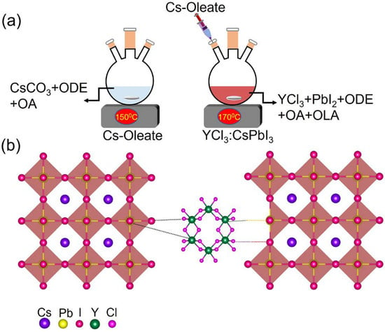
Scheme 1.
(a) Schematic illustration of hot injection method of YCl3:CsPbI3 NRs perovskite. (b) The intentional doping of YCl3 in the CsPbI3 nanocrystals precursor solution. The presence of surface chloride initiates the surface energy imbalance of the unit cell, leading to the anisotropic growth of CsPbI3 NCs.
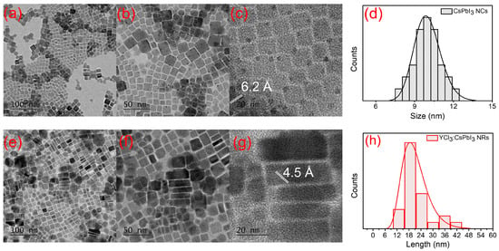
Figure 1.
(a) TEM image, and (b,c) high-resolution TEM (HR-TEM) images of CsPbI3 NCs. (d) The corresponding size distribution histograms. (e) TEM image, and (f,g) HR-TEM images of YCl3-substituted CsPbI3 NRs. (h) The corresponding size distribution histograms.
The X-ray diffraction (XRD) patterns were conducted to ascertain the crystal structure of CsPbI3 NCs and YCl3:CsPbI3 NRs, as shown in Figure 2. Both the CsPbI3 NCs and YCl3:CsPbI3 NRs adhere to the reference pattern of the bulk cubic CsPbI3 perovskite (PDF#98-018-1288), and the diffraction peaks, which appear at 14.02°, 20.03°, 28.407°, 31.88°, 35.45°, 41.05°, and 51.63°, are corresponding to cubic planes of (100), (110), (200), (210), (211), (220), and (300), respectively. As shown in Figure 2b,c, the angles of diffraction peaks for the (100) and (200) planes shifted towards higher values attributed to the reduction in the lattice parameters of YCl3:CsPbI3 NRs, which stemmed from the partial substitution lead cation (Pb2+) and iodide ions (I−) with Y3+ cation and Cl− ions, respectively [12,24]. The scanning electron microscopy (SEM) images of the unsubstituted and YCl3-substituted CsPbI3 NCs are illustrated in Figure 2d,e. Contrary to perovskite NCs, the SEM image of (YCl3-substituted CsPbI3) nanorods are homogeneously distributed on the glass substrate, which indicates that the nanorod film layer has a good foundation for electroluminescence devices.
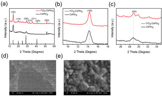
Figure 2.
(a) X-ray diffraction pattern for the unsubstituted and YCl3-substituted CsPbI3 NCs’ thin film, and (b,c) enlarged XRD data of the diffraction peaks of (100) and (200) planes. (d,e) the scanning electron microscopy (SEM) images of the unsubstituted and YCl3-substituted CsPbI3 NCs.
X-ray photoelectron spectra (XPS) analysis was performed to gain insight into the interaction of YCl3 with CsPbI3 nanocrystals (NCs), and the results are presented in Figure 3a. The characteristic XPS signals for Cs 3d, Pb 4f, I 3d, Y 3d, and Cl 2p were observed in YCl3-doped CsPbI3 NCs and N 1s, O 1s, and C 1s signals coupled with native ligand bonding. The high-resolution XPS spectra of Cs 3d, Pb 4f, I 3d, Y 3d, and Cl 2p are displayed in the order in Figure 3b–f. The partial substitution of I− ions by Cl− ions is evidenced by an increase in the binding energies of Pb2+ 4f5/2 and Pb2+ 4f7/2 from 143.56 and 138.37 eV to 143.64 and 138.7 eV, respectively. The binding energy of I 3d and Cs 3d displays little variation compared to YCl3:CsPbI3 nanocrystals (NCs). More importantly, the binding energy signals of Y3+ and Cl− can be observed in the YCl3-substituted CsPbI3 nanorods (NRs). These findings provide additional evidence supporting the partial substitution of iodide ions by chloride ions [25].
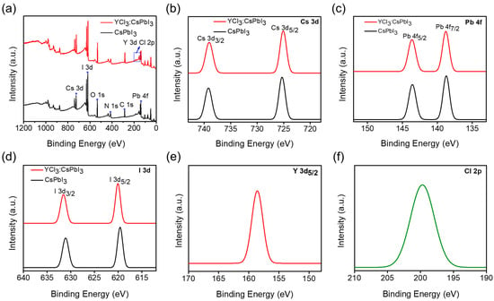
Figure 3.
(a) X-ray photoelectron spectroscopy (XPS) of CsPbI3 NCs and YCl3:CsPbI3 NRs. High-resolution XPS spectra of (b) Cs 3d, (c) Pb 4f, and (d) I 3d of pristine CsPbI3 NCs and YCl3:CsPbI3 NRs. (e,f) Y 3d and Cl 2p spectra of YCl3-substituted CsPbI3 NRs thin film.
To gain a better understanding of the effects of the partial substitution of Pb2+ cation and iodide ions (I−) with yttrium cation (Y3+) and chloride (Cl−) ions, the optical properties of both as-synthesized CsPbI3 nanocrystals (NCs) and YCl3:CsPbI3 nanorods (NRs) were analyzed (Figure 4). The corresponding normalized PL and absorption spectra of YCl3:CsPbI3 NRs showed that the peak position exhibited a blue shift owing to the introduction of chloride (Cl−) ions (Figure 4a,b) [26]. The enlarged bandgap caused the blue shifts of the absorption and PL spectra for YCl3:CsPbI3 NRs due to the partial replacement of lead (Pb2+) cation and iodide (I−) ions with yttrium cation (Y3+) and chloride (Cl−) ions [27]. The blue dots in Figure 4b demonstrate the blue shift associated with introducing YCl3 into the CsPbI3 perovskite. The Tauc plot of the unsubstituted and YCl3-substituted CsPbI3 NC films is illustrated in Figure 4c,d, and the corresponding band value of the unsubstituted is 1.76 eV, and the YCl3-substituted is 1.82 eV. The PLQY increased from 51% to 70% for the YCl3 passivated CsPbI3 NCs, suggesting enhanced radiative recombination followed by yttrium chloride doping (Figure 4e). The environmental durability of the YCl3:CsPbI3 solution was noticeably enhanced (Figure 4f), and the YCl3-substituted CsPbI3 NRs maintained (50% out of 70%) a PLQY, with a loss of 28% PLQY after being stored for 45 days under ambient conditions, prized for the effectiveness of yttrium chloride passivation. However, over the same period of time, the PL quantum yield of pristine CsPbI3 NCs nearly approached zero. The inset of Figure 4f shows the images recorded at different times for the unsubstituted and YCl3-substituted CsPbI3 NC solution.
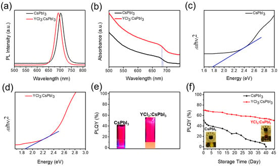
Figure 4.
(a,b) Photoluminescence (PL) and absorption spectra of the unsubstituted and YCl3-substituted CsPbI3 NCs. (c,d) Tauc plot of the unsubstituted and YCl3-substituted CsPbI3 NCs, and (e) PL-quantum yield (PLQY) of the unsubstituted and YCl3-substituted CsPbI3 NCs. The inset (e) is the image of the CsPbI3 NC and YCl3:CsPbI3 NR solution under the UV lamp. (f) PLQY values as a function of stored days for unsubstituted (51 ± 0.5%) and YCl3-substituted (70 ± 1%) CsPbI3 NC solution. The inset is real images of both samples after 45 days.
The control and YCl3-substituted CsPbI3 NCs were employed as emitters to evaluate the potential applications in perovskite LEDs. The LEDs were fabricated based on the configuration of indium tin oxide (ITO)/poly(3,4-ethylenedioxythiophene) polystyrenesulfonate (PEDOT:PSS)/poly(4-butylphenyl-diphenyl-amine) (P-TPD)/unsubstituted CsPbI3 or YCl3:CsPbI3/1,3,5-tris(1-phenyl-1H-benzimidazol-2-yl)benzene (TPBi)/lithium fluoride (LiF)/aluminum (Al). The schematic illustration of PeLED and the corresponding energy levels diagram of the functional layer are illustrated in Figure 5a,b. The functional layers’ energy level values are taken from previous literature [12]. The thickness of ITO (150 nm), PEDOT: PSS, P-TPD (60 nm), YCl3:CsPbI3 (55 nm), TPBi (60 nm), and LiF/Al (130 nm) were analyzed by the cross-sectional TEM image, as shown in Figure 5c. The current density-voltage-luminance (J-V-L) curves of the unsubstituted and YCl3-substituted CsPbI3 NC LEDs with a 4 mm2 emitting area are displayed in Figure 5d. The turn-on voltage (where the luminance achieved 1 cd/m2) is reduced from ~3.9 V to ~3.6 V for the YCl3-substituted CsPbI3 NC LED, revealing that more balanced carriers injected owing to their matched energy level with the carrier transfer layer and enhanced conductivity induced by the YCl3-substitution that facilitated the efficient charges’ injection [12,23]. The CsPbI3 NC and YCl3:CsPbI3 NR-based LEDs showed a maximum luminance of 263.1 cd/m2 and 421.8 cd/m2, respectively. The electroluminescence (EL) spectra of the unsubstituted and YCl3-substituted CsPbI3 NC LEDs were observed at 691 nm and 688 nm (Figure 5e). The values are quite different from the PL spectra in the case of the unsubstituted one (Figure 4a). The similar EL spectra of the two devices are attributed to the weak microcavity effect in the LED structure, which is related to the recombination zone of the device. The recombination zone would be at the interface of EML and ETL in both cases due to the dominance of the hole carrier in perovskite EMLs. The YCl3:CsPbI3-based LEDs revealed high color purity with Commission internationale de l’éclairage (CIE) coordinates of (0.71, 0.26), corresponding to the BT. 2020 color gamut, as shown in Figure 5f. The EQE vs. luminance curves are displayed in Figure 5g. The peak EQE of YCl3:CsPbI3 is 3.16%, 1.86-fold higher than the pristine CsPbI3 NC (1.69%) based LED. This enhancement is attributed to enhanced PLQY and more balanced carrier transfer in the YCl3:CsPbI3 EML layer.
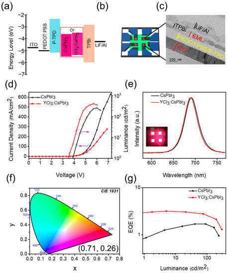
Figure 5.
(a) Schematic flat band energy diagram of perovskite LEDs. (b,c) Schematic device illustration and the corresponding cross-sectional TEM image of the perovskite LEDs. (d) Current density-voltage and luminance-voltage curves, (e) EL spectra of the unsubstituted and YCl3-substituted CsPbI3 LED device. The inset shows the image of a working YCl3-substituted CsPbI3 LED device. (f) the CIE coordinate of YCl3-substituted CsPbI3 LED, (0.71, 0.26). (g) EQE-Luminance curves of the unsubstituted and YCl3-substituted CsPbI3 LED device.
To further investigate the enhanced EQE in the YCl3-substituted CsPbI3 NRs, we conducted angle-dependent photoluminescence (ADPL) measurements to probe the orientation of transition dipole moments (TDMs) in assembled thin film of CsPbI3 nanocrystals/nanorods. The outcoupling efficiency in PeLEDs has the potential for improvement through controlling the orientation of TDMs [28,29,30]. The optical TDMs of nanoplatelets and nanorods are highly anisotropic, and outcoupling efficiency in planer PeLEDs is profoundly associated with the orientation of emissive TDMs [15,17]. The orientation of the optical TDMs of the unsubstituted and YCl3-substituted CsPbI3 NCs were measured by the ratio of horizontal TDMs (Θ). The experimental data are fitted to the pattern simulated, employing the classical dipole radiation model [31]. The Θ values of CsPbI3 NCs’ and YCl3:CsPbI3 NRs’ films are determined to be 67% and 75% (Figure 6a,b). The Θ value in anisotropic nanorods is considerably higher than that in isotropic nanocrystals. Thus, the optical TDMs that are horizontally oriented in anisotropic nanorods are preferred for light outcoupling, resulting in the improved EQE of the LEDs.
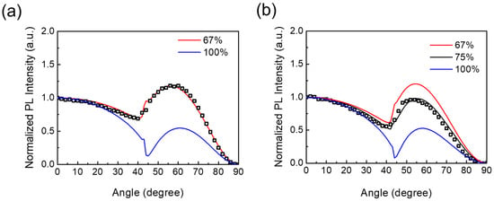
Figure 6.
Angle-dependent PL measurements of the perovskite film on a quartz substrate/nanocrystal or nanorods. The experimental data (black squares) are fitted by the classical electromagnetic dipole model, giving a horizontal TDM ratio of (a) CsPbI3 NCs 67%, and (b) YCl3-substituted CsPbI3 NRs 75%.
4. Conclusions
In this study, we investigated the effects of incorporating metal chloride (YCl3) into CsPbI3 nanocrystals to control the dimensions. We found that the incorporation of YCl3 led to a decrease in the lattice parameters of the CsPbI3 nanocrystals, which resulted from the partial substitution of larger lead cation (Pb2+) and iodide (I−) ions with smaller Y3+ and Cl− ions. The presence of Cl− ions on the surface of the NCs, coupled with the difference in bond energies between chloride (Cl−) and iodide (I−) ions, led to the anisotropic formation of the CsPbI3 nanocrystals into one-dimensional (1D) nanorods. The YCl3 also significantly improved the photoluminescence quantum yield and storage lifetime of the perovskite solution by passivating nonradiative recombination rates and defects properly. Finally, we used the YCl3-substituted CsPbI3 nanorods as the emissive layer in red LEDs and observed a significant improvement in their performance. The LEDs exhibited an external quantum efficiency of 3.16% which is 1.86-fold higher than the pristine CsPbI3 NC (1.69%) based LED, attributed to the improvement of the ratio of horizontal TDMs in the anisotropic YCl3:CsPbI3 nanorods to 75% from 67% of that of NCs. Overall, the combined characteristics of YCl3-substituted CsPbI3 nanorods show great potential for developing stable and efficient red LEDs.
Author Contributions
M.I.S.: conceptualization, investigation, data analysis and writing—original draft preparation; A.K.: device fabrication; A.A.: angle dependent PL analysis; S.-H.J. and J.-H.L.: characterization; J.-H.L.: conceptualization, writing—review and editing, supervision, funding acquisition. All authors have read and agreed to the published version of the manuscript.
Funding
This research was supported by Basic Science Research Program through the National Research Foundation of Korea (NRF) funded by the Ministry of Education (2022R1A6A1A03051705). This work was also supported by an Inha University Research Grant (No. 65380-1).
Data Availability Statement
Data will be made available upon request.
Acknowledgments
The authors would like to acknowledge Siwei He from the Department of Flexible and Printable Electronics (LANL-CBNU Engineering Institute, Korea, Jeonbuk National University) for Cs-corrected TEM measurement. In addition, we acknowledge the financial support provided by Basic Science Research Program through the National Research Foundation of Korea (NRF) funded by the Ministry of Education (2022R1A6A1A03051705). This work was also supported by an Inha University Research Grant (No. 65380-1).
Conflicts of Interest
There is no conflict of interest.
References
- Kim, Y.-H.; Kim, S.; Kakekhani, A.; Park, J.; Park, J.; Lee, Y.-H.; Xu, H.; Nagane, S.; Wexler, R.B.; Kim, D.-H.; et al. Comprehensive defect suppression in perovskite nanocrystals for high-efficiency light-emitting diodes. Nat. Photon. 2021, 15, 148–155. [Google Scholar] [CrossRef]
- Yang, J.-N.; Chen, T.; Ge, J.; Wang, J.-J.; Yin, Y.-C.; Lan, Y.-F.; Ru, X.-C.; Ma, Z.-Y.; Zhang, Q.; Yao, H.-B. High Color Purity and Efficient Green Light-Emitting Diode Using Perovskite Nanocrystals with the Size Overly Exceeding Bohr Exciton Diameter. J. Am. Chem. Soc. 2021, 143, 19928–19937. [Google Scholar] [CrossRef] [PubMed]
- Raja, S.N.; Bekenstein, Y.; Koc, M.A.; Fischer, S.; Zhang, D.; Lin, L.; Ritchie, R.O.; Yang, P.; Alivisatos, A.P. Encapsulation of Perovskite Nanocrystals into Macroscale Polymer Matrices: Enhanced Stability and Polarization. ACS Appl. Mater. Interfaces 2016, 8, 35523–35533. [Google Scholar] [CrossRef] [PubMed]
- Konidakis, I.; Karagiannaki, A.; Stratakis, E. Advanced composite glasses with metallic, perovskite, and two-dimensional nanocrystals for optoelectronic and photonic applications. Nanoscale 2022, 14, 2966–2989. [Google Scholar] [CrossRef]
- Shen, X.; Wang, Z.; Tang, C.; Zhang, X.; Lee, B.R.; Li, X.; Li, D.; Zhang, Y.; Hu, J.; Zhao, D.; et al. Near-Infrared LEDs Based on Quantum Cutting-Activated Electroluminescence of Ytterbium Ions. Nano Lett. 2023, 23, 82–90. [Google Scholar] [CrossRef]
- Wang, Y.; Yuan, F.; Dong, Y.; Li, J.; Johnston, A.; Chen, B.; Saidaminov, M.I.; Zhou, C.; Zheng, X.; Hou, Y.; et al. All-Inorganic Quantum-Dot LEDs Based on a Phase-Stabilized α-CsPbI 3 Perovskite. Angew. Chem. Int. Ed. 2021, 60, 16164–16170. [Google Scholar] [CrossRef]
- Polavarapu, L.; Nickel, B.; Feldmann, J.; Urban, A.S. Advances in Quantum-Confined Perovskite Nanocrystals for Optoelectronics. Adv. Energy Mater. 2017, 7, 1700267. [Google Scholar] [CrossRef]
- Tang, C.; Shen, X.; Yu, S.; Zhong, Y.; Wang, Z.; Hu, J.; Lu, M.; Wu, Z.; Zhang, Y.; Yu, W.W.; et al. Post-treatment of CsPbI3 nanocrystals by p-iodo-D-Phenylalanine for efficient perovskite LEDs. Mater. Today Phys. 2021, 21, 100555. [Google Scholar] [CrossRef]
- Bi, C.; Hu, J.; Yao, Z.; Lu, Y.; Binks, D.; Sui, M.; Tian, J. Self-Assembled Perovskite Nanowire Clusters for High Luminance Red Light-Emitting Diodes. Adv. Funct. Mater. 2020, 30, 2005990. [Google Scholar] [CrossRef]
- Saleem, M.I.; Yang, S.; Zhi, R.; Li, H.; Sulaman, M.; Chandrasekar, P.V.; Zhang, Z.; Batool, A.; Zou, B. Self-powered, all-solution processed, trilayer heterojunction perovskite-based photodetectors. Nanotechnology 2020, 31, 254001. [Google Scholar] [CrossRef]
- Ji, R.; Zhang, Z.; Hofstetter, Y.J.; Buschbeck, R.; Hänisch, C.; Paulus, F.; Vaynzof, Y. Perovskite phase heterojunction solar cells. Nat. Energy 2022, 7, 1170–1179. [Google Scholar] [CrossRef]
- Pan, G.; Bai, X.; Shen, X.; Wang, L.; Mao, Y.; Chen, X.; Xu, W.; Shao, H.; Zhou, D.; Dong, B.; et al. Bright red YCl3-promoted CsPbI3 perovskite nanorods towards efficient light-emitting diode. Nano Energy 2021, 81, 105615. [Google Scholar] [CrossRef]
- Tong, Y.; Bladt, E.; Aygüler, M.F.; Manzi, A.; Milowska, K.Z.; Hintermayr, V.A.; Docampo, P.; Bals, S.; Urban, A.S.; Polavarapu, L.; et al. Highly Luminescent Cesium Lead Halide Perovskite Nanocrystals with Tunable Composition and Thickness by Ultrasonication. Angew. Chem. Int. Ed. 2016, 55, 13887–13892. [Google Scholar] [CrossRef] [PubMed]
- Yang, D.; Li, P.; Zou, Y.; Cao, M.; Hu, H.; Zhong, Q.; Hu, J.; Sun, B.; Duhm, S.; Xu, Y.; et al. Interfacial Synthesis of Monodisperse CsPbBr3 Nanorods with Tunable Aspect Ratio and Clean Surface for Efficient Light-Emitting Diode Applications. Chem. Mater. 2019, 31, 1575–1583. [Google Scholar] [CrossRef]
- Cui, J.; Liu, Y.; Deng, Y.; Lin, C.; Fang, Z.; Xiang, C.; Bai, P.; Du, K.; Zuo, X.; Wen, K.; et al. Efficient light-emitting diodes based on oriented perovskite nanoplatelets. Sci. Adv. 2021, 7, eabg8458. [Google Scholar] [CrossRef]
- Jurow, M.J.; Morgenstern, T.; Eisler, C.; Kang, J.; Penzo, E.; Do, M.; Engelmayer, M.; Osowiecki, W.T.; Bekenstein, Y.; Tassone, C.; et al. Manipulating the Transition Dipole Moment of CsPbBr3 Perovskite Nanocrystals for Superior Optical Properties. Nano Lett. 2019, 19, 2489–2496. [Google Scholar] [CrossRef]
- Walters, G.; Haeberlé, L.; Quintero-Bermudez, R.; Brodeur, J.; Kéna-Cohen, S.; Sargent, E.H. Directional Light Emission from Layered Metal Halide Perovskite Crystals. J. Phys. Chem. Lett. 2020, 11, 3458–3465. [Google Scholar] [CrossRef]
- Hoang, M.T.; Pannu, A.S.; Yang, Y.; Madani, S.; Shaw, P.; Sonar, P.; Tesfamichael, T.; Wang, H. Surface Treatment of Inorganic CsPbI3 Nanocrystals with Guanidinium Iodide for Efficient Perovskite Light-Emitting Diodes with High Brightness. Nano-Micro Lett. 2022, 14, 69. [Google Scholar] [CrossRef]
- Kim, Y.-H.; Zhai, Y.; Lu, H.; Pan, X.; Xiao, C.; Gaulding, E.A.; Harvey, S.P.; Berry, J.J.; Vardeny, Z.V.; Luther, J.M.; et al. Chiral-induced spin selectivity enables a room-temperature spin light-emitting diode. Science 2021, 371, 1129–1133. [Google Scholar] [CrossRef]
- Li, H.; Lin, H.; Ouyang, D.; Yao, C.; Li, C.; Sun, J.; Song, Y.; Wang, Y.; Yan, Y.; Wang, Y.; et al. Efficient and Stable Red Perovskite Light-Emitting Diodes with Operational Stability >300 h. Adv. Mater. 2021, 33, e2008820. [Google Scholar] [CrossRef]
- Tang, Y.; Cao, X.; Honarfar, A.; Abdellah, M.; Chen, C.; Avila, J.; Asensio, M.-C.; Hammarström, L.; Sa, J.; Canton, S.E.; et al. Inorganic Ions Assisted the Anisotropic Growth of CsPbCl3 Nanowires with Surface Passivation Effect. ACS Appl. Mater. Interfaces 2018, 10, 29574–29582. [Google Scholar] [CrossRef] [PubMed]
- Protesescu, L.; Yakunin, S.; Bodnarchuk, M.I.; Krieg, F.; Caputo, R.; Hendon, C.H.; Yang, R.X.; Walsh, A.; Kovalenko, M.V. Nanocrystals of Cesium Lead Halide Perovskites (CsPbX3, X = Cl, Br, and I): Novel Optoelectronic Materials Showing Bright Emission with Wide Color Gamut. Nano Lett. 2015, 15, 3692–3696. [Google Scholar] [CrossRef] [PubMed]
- Lu, M.; Guo, J.; Sun, S.; Lu, P.; Wu, J.; Wang, Y.; Kershaw, S.V.; Yu, W.W.; Rogach, A.L.; Zhang, Y. Bright CsPbI3 Perovskite Quantum Dot Light-Emitting Diodes with Top-Emitting Structure and a Low Efficiency Roll-Off Realized by Applying Zirconium Acetylacetonate Surface Modification. Nano Lett. 2020, 20, 2829–2836. [Google Scholar] [CrossRef] [PubMed]
- Zhu, Y.; Zhao, J.; Yang, G.; Xu, X.; Pan, G. Ammonium acetate passivated CsPbI3 perovskite nanocrystals for efficient red light-emitting diodes. Nanoscale 2020, 12, 7712–7719. [Google Scholar] [CrossRef] [PubMed]
- Pan, G.; Bai, X.; Yang, D.; Chen, X.; Jing, P.; Qu, S.; Zhang, L.; Zhou, D.; Zhu, J.; Xu, W.; et al. Doping Lanthanide into Perovskite Nanocrystals: Highly Improved and Expanded Optical Properties. Nano Lett. 2017, 17, 8005–8011. [Google Scholar] [CrossRef] [PubMed]
- Yao, J.-S.; Ge, J.; Wang, K.-H.; Zhang, G.; Zhu, B.-S.; Chen, C.; Zhang, Q.; Luo, Y.; Yu, S.-H.; Yao, H.-B. Few-Nanometer-Sized α-CsPbI3 Quantum Dots Enabled by Strontium Substitution and Iodide Passivation for Efficient Red-Light Emitting Diodes. J. Am. Chem. Soc. 2019, 141, 2069–2079. [Google Scholar] [CrossRef] [PubMed]
- Xia, W.; Ren, Z.; Zheng, Z.; Luo, C.; Li, J.; Ma, W.; Zhou, X.; Chen, Y. Highly stable lanthanide-doped CsPbI3 perovskite nanocrystals with near-unity quantum yield for efficient red light-emitting diodes. Nanoscale 2023, 15, 1109–1118. [Google Scholar] [CrossRef]
- Jeon, S.; Zhao, L.; Jung, Y.-J.; Kim, J.W.; Kim, S.-Y.; Kang, H.; Jeong, J.-H.; Rand, B.P.; Lee, J.-H. Perovskite Light-Emitting Diodes with Improved Outcoupling Using a High-Index Contrast Nanoarray. Small 2019, 15, 1900135. [Google Scholar] [CrossRef]
- He, S.; Kumar, N.; Beng Lee, H.; Ko, K.-J.; Jung, Y.-J.; Il Kim, J.; Bae, S.; Lee, J.-H.; Kang, J.-W. Tailoring the refractive index and surface defects of CsPbBr3 quantum dots via alkyl cation-engineering for efficient perovskite light-emitting diodes. Chem. Eng. J. 2021, 425, 130678. [Google Scholar] [CrossRef]
- Jurow, M.J.; Lampe, T.; Penzo, E.; Kang, J.; Koc, M.A.; Zechel, T.; Nett, Z.; Brady, M.; Wang, L.-W.; Alivisatos, A.P.; et al. Tunable Anisotropic Photon Emission from Self-Organized CsPbBr3 Perovskite Nanocrystals. Nano Lett. 2017, 17, 4534–4540. [Google Scholar] [CrossRef]
- Barnes, W.L. Fluorescence near interfaces: The role of photonic mode density. J. Mod. Opt. 1998, 45, 661–699. [Google Scholar] [CrossRef]
Disclaimer/Publisher’s Note: The statements, opinions and data contained in all publications are solely those of the individual author(s) and contributor(s) and not of MDPI and/or the editor(s). MDPI and/or the editor(s) disclaim responsibility for any injury to people or property resulting from any ideas, methods, instructions or products referred to in the content. |
© 2023 by the authors. Licensee MDPI, Basel, Switzerland. This article is an open access article distributed under the terms and conditions of the Creative Commons Attribution (CC BY) license (https://creativecommons.org/licenses/by/4.0/).